DATA SHEET
www.onsemi.com
PWM Buck Controller,
Synchronous, 100V
MARKING
DIAGRAM
SOIC−16
D SUFFIX
CASE 751B
NCP1034
NCP1034DG
AWLYWW
Description
The NCP1034 is a high voltage PWM controller designed for high
performance synchronous Buck DC/DC applications with input
voltages up to 100 V. The NCP1034 drives a pair of external
N−MOSFETs. The switching frequency is programmable from
25 kHz up to 500 kHz allowing the flexibility to tune for efficiency
and size. A synchronization feature allows the switching frequency to
be set by an external source or output a synchronization signal to
multiple NCP1034 controllers. The output voltage can be precisely
regulated using the internally trimmed 1.25 V reference voltage for
low voltage applications. Protection features include user
programmable undervoltage lockout and hiccup current limit.
Features
•
•
•
•
•
•
•
•
•
•
•
High Voltage Operating up to 100 V
Programmable Switching Frequency up to 500 kHz
2 A Output Drive Capability
Precision Reference Voltage (1.25 V)
Programmable Soft−Start with Prebiased Load Capability
Programmable Overcurrent Protection
Programmable Undervoltage Protection
Hiccup Current Limit Using MOSFET RDS(on) Sensing
External Frequency Synchronization
16 Pin SOIC Package
This is a Pb−Free Device
A
WL
Y
WW
G
= Assembly Location
= Wafer Lot
= Year
= Work Week
= Pb−Free Package
PIN CONNECTIONS
OCset 1
16 UVLO
FB 2
15 RT
Comp 3
14 GND
SS/SD 4
13 OCIN
SYNC 5
12 VCC
PGND 6
11 VS
LDRV 7
10 HDRV
DRVCC 8
9 VB
(Top View)
ORDERING INFORMATION
See detailed ordering and shipping information in the package
dimensions section on page 24 of this data sheet.
Applications
•
•
•
•
•
48 V Non−Isolated DC−DC Converter
Embedded Telecom Systems
Networking and Computing Voltage Regulator
Distributed Point of Load Power Architectures
General High Voltage DC−DC Converters
© Semiconductor Components Industries, LLC, 2015
November, 2021 − Rev. 15
1
Publication Order Number:
NCP1034/D
�NCP1034
VIN: 48 V
VCC: 12 V
R4
110k
C2
C3
100n
100n
D1
1N4148
8
12
R10
5
10k
15
GND
4
16
1
14
R5
3k9
GND
C5
220n
R6
20k
GND GND
R7
11k
GND
VCC
SYNC
C4
9
DRVVCC VB
HDRV
VS
10
R8
7
10k
SS/SD
LDRV
UVLO
PGND
6
FB
2
COMP
3
GND
IC1
NCP1034
Q1
NTD3055
L1
13
OCIN
C1B
2u2
GND
100n
11
RT
OCSET
C1A
2u2
13�
Q2
NTD24N06
VOUT
5 V @ 5 A, 200 kHz
C9
C9B
C9C
47�
47�
47�
R1
16k9
R9
1k2
C8
1n8
C6
R3
4k7
12n
C7
330p
GND
Figure 1. Typical Application Circuit
www.onsemi.com
2
R2
5k6
GND
(For applications operating
at cold ambient temperatures refer to the soft−start
section on Page 15)
�3
www.onsemi.com
Figure 2. Internal Block Diagram
OCset
Comp
Fb
1.25V
SS/SD
Rt
SYNC
UVLO
GND
1uA
POR
Iocset
25k
OCP
OCP
VBIAS
20uA
Vref
Error Amp
SS/SD
Vref
R
S
64uA Max
0.3V
Ct
Rt Oscillator
Vcc UVLO
PWM
LowUVLO
POR
OCP
Positive
Current
PWM
DR
Clk
FAULT
TONMIN
Limit
POR
1.25V = Vref
5V = VBIAS
MKO
350ns
Reset Dom
Error
Comparator
Q
Bias
Generator
Q
AC ON
FAULT
VCC
Delay
LS
R
S
Q
AC ON
VBIAS
VBIAS
0.225x Iocset
0.0410x Iocset
OCP Reset
OCP Q
Negative
Output
S
R
UV
LowUVLO
UV
Detect
UV
Detect
Positive Current
SS/SD
0.25V
FAULT
High
Voltage
Level
Shift
Circuit
Active
Clamp
AC ON
OCin
PGND
LDrv
DrvVCC
Vs
HDrv
Vb
NCP1034
�NCP1034
PIN FUNCTION DESCRIPTION
PIN
PIN NAME
1
OCset
DESCRIPTION
2
FB
3
COMP
Output of error amplifier. An external resistor and capacitor network is typically connected from this pin to ground
to provide loop compensation.
4
SS/SD
Soft−Start / Shutdown. This pin provides user programmable soft−start function. External capacitor connected
from this pin to ground sets the startup time of the output voltage. The converter can be shutdown by pulling this
pin below 0.3 V.
5
SYNC
The internal oscillator can be synchronized to an external clock via this pin and other IC’s can be synchronized
via this pin to internal oscillator. If it is not used this pin should be connected via 10 k� resistor to ground.
6
PGND
Power Ground. This pin serves as a separate ground for the MOSFET driver and should be connected to the
system’s power ground plane.
7
LDRV
Output driver for low side MOSFET.
8
DRVVCC
This pin provides biasing for the internal low side driver. A minimum of 0.1 �F, high frequency capacitor must be
connected from this pin to power ground.
9
VB
This pin powers the high side driver and must be connected to a voltage higher than input voltage. A minimum of
0.1 �F, high frequency capacitor must be connected from this pin to switch node.
10
HDRV
11
VS
12
VCC
This pin provides power for the internal blocks of the IC. A minimum of 0.1 �F, high frequency capacitor must be
connected from this pin to ground.
13
OCIN
Overcurrent sensing input. A serial resistor from this pin to drain of low MOSFET must be used to limit the
current into this pin.
14
GND
Signal ground for internal reference and control circuitry.
15
RT
16
UVLO
Current limit set point. A resistor from this pin to GND will set the positive and negative current limit threshold
Inverting input to the error amplifier. This pin is connected directly to the output of the regulator via resistor
divider to set the output voltage and provide feedback to the error amplifier.
Output driver for high side MOSFET
Switch Node. This pin is connected to the source of the upper MOSFET and the drain of the lower MOSFET.
This pin is return path for the upper gate driver.
Connecting a resistor from this pin to ground sets the oscillator frequency.
An external voltage divider is used to set the undervoltage threshold levels.
www.onsemi.com
4
�NCP1034
ABSOLUTE MAXIMUM RATINGS
Min
Max
Unit
FB, VUVLO, RT, OCset
Rating
Symbol
−0.3
10
V
COMP, SS/SD, SYNC, OCIN
−0.3
6
V
LDRV
−0.3
VCC + 0.3
V
DRVVCC, VCC
−0.3
20
V
VS
VS + 20
V
VS − 0.3
VB + 0.3
V
−1.0
150
V
20
mA
VB
HDRV
VS
OCin Input Current
All voltages referenced to GND
Rating
Thermal Resistance, Junction−to−Ambient
Operating Ambient Temperature Range
Symbol
Value
Unit
R�JA
130
°C/W
TA
−40 to 125
°C
TSTG
−55 to 150
°C
Junction Operating Temperature
TJ
−40 to 150
°C
ESD Withstand Voltage (Note 1)
Human Body Model
Machine Model
VESD
2000
200
V
V
Storage Temperature Range
Latchup Capability per Jedec JESD78
Stresses exceeding those listed in the Maximum Ratings table may damage the device. If any of these limits are exceeded, device functionality
should not be assumed, damage may occur and reliability may be affected.
1. Excluding pins Vb, VS and HDRV.
TYPICAL ELECTRICAL PARAMETERS
RECOMMENDED OPERATING CONDITIONS
Symbol
Definition
Min
Max
Unit
100
V
VIN
Converting Voltage
VCC
Supply Voltage
10
18
V
DRVCC
Supply Voltage
10
18
V
VB to VS
Supply Voltage
10
18
V
FSW
Operating Frequency
25
500
kHz
TJ
Junction Temperature
−40
125
°C
Functional operation above the stresses listed in the Recommended Operating Ranges is not implied. Extended exposure to stresses beyond
the Recommended Operating Ranges limits may affect device reliability.
www.onsemi.com
5
�NCP1034
ELECTRICAL CHARACTERISTICS (Unless otherwise specified, these specifications apply over VCC = 12 V,
DRVVCC = VB = 12 V, −40°C < TJ < 125°C)
Parameter
Symbol
Test Condition
Min
Typ
Max
Unit
REFERENCE VOLTAGE
Feedback Voltage
VFB
Accuracy
1.25
+1.5
%
2.0
mV
2.0
3.0
mA
SS = 0 V, No Switching
0.1
0.3
mA
IB(Static)
SS = 0 V, No Switching
0.1
0.3
mA
VCC−Start−Threshold
VCC_UVLO (R)
Supply Ramping Up
7.9
8.9
9.8
V
VCC−Stop−Threshold
VCC_UVLO (F)
Supply Ramping Down
7.3
8.2
9.0
V
FB Voltage Line Regulation
−40°C < TJ < 125°C
LREG
10 V < VCC < 18 V (Note 3)
VCC Supply Current (Stat)
ICC(Static)
SS = 0 V, No Switching, RT = 10 k�,
ROCSET = 10 k�
DRVVCC Supply Current (Stat)
IC(Static)
VB Supply Current (Stat)
−1.5
V
SUPPLY CURRENT
UNDERVOLTAGE LOCKOUT
VCC−Hysteresis
Supply Ramping Up and Down
0.7
V
DRVCC−Start−Threshold
DRVCC_UVLO (R)
Supply Ramping Up
7.9
8.9
9.8
V
DRVCC−Stop−Threshold
DRVCC_UVLO (F)
Supply Ramping Down
7.3
8.2
9.0
V
DRVCC−Hysteresis
Supply Ramping Up and Down
0.7
V
VB−Start−Threshold
VB_UVLO (R)
Supply Ramping Up
7.9
8.9
9.8
V
VB−Stop−Threshold
VB_UVLO (F)
Supply Ramping Down
7.3
8.2
9.0
V
VB−Hysteresis
Supply Ramping Up and Down
0.7
V
Undervoltage Threshold Value
UUVLO (Rising)
1.19
1.25
1.31
V
Undervoltage Threshold Value
UUVLO (Falling)
1.10
1.15
1.20
V
170
320
200
375
230
430
kHz
OSCILLATOR
FS
RT = 20 k�
RT = 10 k�
Ramp Amplitude
Vramp
(Note 3)
Min Duty Cycle
Dmin
FB = 2 V
0
%
Min Pulse Width
Dmin(ctrl)
FS = 200 kHz, (Note 3)
200
ns
Max Duty Cycle
Dmax
FS = 400 kHz, FB = 1.2 V
SYNC(FS)
20% Above Free Running
Frequency
Frequency
SYNC Frequency Range
SYNC Pulse Duration
2.0
V
80
%
500
SYNC(pulse)
200
SYNC High Level
SYNC(H)
2.0
SYNC Low Level
SYNC(L)
kHz
ns
V
0.8
1.6
V
SYNC Input Threshold
SYNC(Thre)
SYNC Input Hysteresis
SYNC(Hyst)
SYNC Input Impedance
SYNC(ZIN)
(Note 3)
16
k�
SYNC Output Impedance
SYNC(OUT)
(Note 3)
2.5
k�
SYNC Output Pulse Width
SYNC(Pulse Width)
FS = 500 kHz, (Note 3)
300
ns
300
V
mV
Product parametric performance is indicated in the Electrical Characteristics for the listed test conditions, unless otherwise noted. Product
performance may not be indicated by the Electrical Characteristics if operated under different conditions.
2. Cold temperature performance is guaranteed via correlation using statistical quality control. Not tested in production.
3. Guaranteed by design but not tested in production.
www.onsemi.com
6
�NCP1034
ELECTRICAL CHARACTERISTICS (Unless otherwise specified, these specifications apply over VCC = 12 V,
DRVVCC = VB = 12 V, −40°C < TJ < 125°C)
Parameter
Symbol
Test Condition
IFB
SS = 3 V, FB = 1 V
Min
Typ
Max
Unit
−0.1
−0.4
�A
50
100
120
�A
4.0
10
MHz
55
dB
ERROR AMPLIFIER
Input Bias Current
Source/Sink Current
I(Source/Sink)
Bandwidth
(Note 3)
DC gain
(Note 3)
Transconductance
gm
(Note 3)
1500
3150
4000
�mho
Soft−Start Current
ISS
SS = 0 V
15
20
25
�A
Shutdown Output Threshold
SD
0.3
0.4
V
OCSET Voltage
VOCSET
1.25
V
Hiccup Current
IHiccup
(Note 3)
1.0
�A
Hiccup(duty)
IHiccup/ISS, (Note 3)
tr(Lo)
CL = 1.5 nF (See Figure 3)
17
ns
HI Drive Rise Time
tr(Hi)
CL = 1.5 nF (See Figure 3)
17
ns
LO Drive Fall Time
tf(Lo)
CL = 1.5 nF (See Figure 3)
10
ns
HI Drive Fall Time
tf(Hi)
CL = 1.5 nF (See Figure 3)
10
ns
Dead Band Time
tdead
(See Figure 3)
LO Output High Short Circuit
Pulsed Current
tLDRVhigh
VLDRV = 0 V, PW v 10 �s,
TJ = 25°C (Note 3)
1.4
A
HI Output High Short Circuit
Pulsed Current
tHDRVhigh
VHDRV = 0 V, PW v 10 �s,
TJ = 25°C (Note 3)
2.2
A
LO Output Low Short Circuit
Pulsed Current
tLDRVhigh
VLDRV = DRVVCC, PW v 10 �s,
TJ = 25°C (Note 3)
1.4
A
HI Output Low Short Circuit
Pulsed Current
tHDRVhigh
VHDRV = VB, PW v 10 �s,
TJ = 25°C (Note 3)
2.2
A
LO Output Resistor, Source
RLOH
Typical Value @ 25°C, (Note 3)
7
LO Output Resistor, Sink
RLOL
Typical Value @ 25°C, (Note 3)
HI Output Resistor, Source
RHIH
Typical Value @ 25°C, (Note 3)
HI Output Resistor, Sink
RHIL
Typical Value @ 25°C, (Note 3)
SOFT−START/SD
OVERCURRENT PROTECTION
Hiccup Duty Cycle
5.0
%
OUTPUT DRIVERS
LO, Drive Rise Time
30
60
120
ns
12
�
2
8
�
7
12
�
2
8
�
Product parametric performance is indicated in the Electrical Characteristics for the listed test conditions, unless otherwise noted. Product
performance may not be indicated by the Electrical Characteristics if operated under different conditions.
2. Cold temperature performance is guaranteed via correlation using statistical quality control. Not tested in production.
3. Guaranteed by design but not tested in production.
www.onsemi.com
7
�NCP1034
tr
tf
9V
High−Side
Driver
(HDrv)
2V
tr
tf
9V
Low−Side
Driver
(LDrv)
2V
Deadband
H to L
Deadband
L to H
Figure 3. Definition of Rise−Fall Time and Deadband Time
www.onsemi.com
8
�NCP1034
TYPICAL OPERATING CHARACTERISTICS
1.3
9.0
Rising
8.9
8.8
1.28
UVLOVB (V)
VB (V)
8.7
1.26
1.24
8.6
8.5
8.4
8.3
Falling
8.2
1.22
8.1
8.0
1.2
−40
−20
0
20
40
60
80
100
7.9
−40
120
0
20
40
60
TEMPERATURE (°C)
Figure 4. VFB
Figure 5. UVLOVB
9.2
80
100
120
80
100
120
100
120
9.2
9.1
Rising
9.0
Rising
9.0
UVLODRVVCC (V)
UVLOVCC (V)
−20
TEMPERATURE (°C)
8.8
8.6
8.4
Falling
8.9
8.8
8.7
8.6
8.5
8.4
Falling
8.3
8.2
8.2
8.0
−40
−20
0
20
40
60
80
100
8.1
−40
120
−20
0
20
40
60
TEMPERATURE (°C)
TEMPERATURE (°C)
Figure 6. UVLOVCC
Figure 7. UVLODRVVCC
1.4
2.3
1.35
2.2
Rising
ICC (stat) (mA)
UVLO (V)
1.3
1.25
1.2
Falling
2.0
1.9
1.15
1.1
−40
2.1
−20
0
20
40
60
80
TEMPERATURE (°C)
100
1.8
−40
120
−20
0
20
40
60
TEMPERATURE (°C)
Figure 8. UVLO
Figure 9. ICC (Stat)
www.onsemi.com
9
80
�NCP1034
TYPICAL OPERATING CHARACTERISTICS
220
90
215
88
86
84
205
Dmax (%)
fSW (kHz)
210
200
195
82
80
78
76
190
74
185
72
180
−40
−20
0
20
40
60
80
100
70
−40
120
−20
0
20
40
60
80
100
120
TEMPERATURE (°C)
TEMPERATURE (°C)
Figure 10. Switching Frequency @ RT = 20 kW
Figure 11. Maximum Duty Cycle @ f = 400 kHz
210
4500
205
4000
3500
195
gm (�mho)
tonmin (ns)
200
190
185
3000
2500
180
2000
175
170
−40
−20
0
20
40
60
80
100
1500
−40
120
20
40
60
80
100
120
Figure 12. Minimum on Time
Figure 13. Error Amplifier Transconductance
12
85
11
80
10
75
Low to High
9
R (�)
70
t (ns)
0
TEMPERATURE (°C)
90
65
60
High to Low
DRVVCC = VB = 10 V
8
12 V
7
55
6
50
18 V
5
45
40
−40
−20
TEMPERATURE (°C)
−20
0
20
40
60
80
100
4
−40
120
−20
0
20
40
60
80
100
TEMPERATURE (°C)
TEMPERATURE (°C)
Figure 14. Deadtime
Figure 15. Driver Pullup Resistance
www.onsemi.com
10
120
�NCP1034
TYPICAL OPERATING CHARACTERISTICS
−0.2
4.0
−0.21
3.5
DRVVCC = VB = 10 V
2.5
12 V
18 V
2.0
−0.23
−0.24
−0.25
−0.26
−0.27
−0.28
1.5
−0.29
1.0
−40
−20
0
20
40
60
80
100
−0.3
−40
120
−20
0
20
40
60
80
100
120
TEMPERATURE (°C)
TEMPERATURE (°C)
Figure 16. Driver Pulldown Resistance
Figure 17. OCP @ R8 = 10 kW, ROCIN = 10 kW
0.8
0.7
0.6
VDSLOWFET (V)
R (�)
3.0
VDSLOWFET (V)
−0.22
0.5
0.4
0.3
0.2
0.1
0
−40
−20
0
20
40
60
80
100
TEMPERATURE (°C)
Figure 18. POSOCP @ R8 = 10 kW,
ROCIN = 10 kW
www.onsemi.com
11
120
�NCP1034
APPLICATION INFORMATION
Undervoltage Lock−out
500
There are four undervoltage lock−out circuits. Two of
them protect external high−side and low−side drivers, the
third ensures that the IC does not start until VCC is under a
set threshold. The last one can be programmed by the user.
It has a rising threshold at 1.25 V and a falling threshold at
1.15 V, and the user can define the undervoltage level by an
external resistor divider. If the voltage is not over the
threshold value, the device stops operating. The high−side
driver UVLO only stops switching the high−side MOSFET
Programmed falling and rising UVLO voltage can be
calculated by Equations 1 and 2:
450
ǒ
V UVLO,falling + 1.15 @ 1 )
Ǔ
R4
R5
400
f (kHz)
350
300
250
200
150
100
50
0
(eq. 1)
ǒ
Ǔ
100
150
200
250
Figure 20. Frequency Dependence of Rt Value
(eq. 2)
Frequency Synchronization
The NCP1034 can be synchronized to an external clock
signal. The input synchronization signal should be a TTL
logic level. The oscillator is synchronized to the rising edge
of the synchronizing signal. When synchronization is used,
the free running frequency must be set by the timing resistor
to a frequency at least 80% of the external synchronization
frequency (Example: RT = 20 k� / 200 kHz and external
TTL = 220 kHz).
The NCP1034 can also output synchronization pulses on
the SYNC pin. Pulses are generated when the internal
oscillator ramp reaches the high threshold voltage. The
frequency of these pulses is set by an external RT resistor. Up
to five NCP1034 controllers can be connected directly to the
SYNC pin, all of which are synchronized to the controller
with the highest frequency. The lowest frequency must be at
least 80% of the highest one.
The equivalent internal circuit of the Sync pin is shown in
Figure 21.
Shutdown
The output voltage can be disabled by pulling the
SS/SD pin below 0.3 V. A small transistor can be used to pull
it down as shown in Figure 19. During this time, both
external MOSFETs are turned off. After the SS/SD pin is
released, the IC starts its operation with a soft−start
sequence.
SS/SD
50
Rt (k�)
and
R4
V UVLO,rising + 1.25 @ 1 )
R5
0
SS/SD
Figure 19. Shutdown Interface
VBIAS
Operating Frequency Selection
The operating frequency is set by an external resistor
connected from the Rt Pin to ground. The value of this
resistor can be selected from Figure 20, which shows
switching frequency versus the timing resistor value.
SYNC
Rt
Rt
Oscillator
Ct
Figure 21. Equivalent Connection of the Sync Pin
www.onsemi.com
12
�NCP1034
Figure 22 shows the part with no synchronization. In this
circuit the internal clock is fixed by the external timing
resistor RT. The SYNC pin can be tied to GND through a
series resistor to prevent false triggering in a noisy
environment.
SYNC
SYNC
NCP1034
(Master #1)
NCP1034
(Slave #1)
RT
RT
FSW = 200 kHz
20 k�
SYNC
10 k�
(optional)
FSW = 180 kHz
22 k�
SYNC
NCP1034
NCP1034
(Slave #2)
Synchronized System
Frequency = 200 kHz
RT
RT
FSW = 180 kHz
20 k�
FSW = 200 kHz
22 k�
Figure 22. Fixed Frequency
Figure 24. Master Slave Synchronization
Figure 23 shows the part synchronized to an external
clock through the SYNC pin. The synchronization
frequency can be up to 20% greater then the programmed
fixed frequency (Example: RT = 20 k� / 200 kHz and the
SYNC input frequency can range from 200−220 kHz). The
clock frequency at the SYNC pin replaces the master clock
generated by the internal oscillator circuit. Pulling the
SYNC pin low programs the part to run freely at the
frequency programmed by RT. When pulling the SYNC pin
low a 4.7 kΩ resistor should be used.
Output Voltage
Output voltage can be set by an external resistor divider
according to this Equation 3:
ǒ
V OUT + V ref @ 1 )
Ǔ
R1
R2
(eq. 3)
Where Vref is the internal reference voltage 1.25 V. Absolute
values of resistors R1 and R2 depend on compensation
network type. See compensation paragraph for details.
Inductor Selection
TTL
Logic
4.7 k�
(optional)
The inductor selection is based on the output power,
frequency, input and output voltage and efficiency
requirements. High inductor values cause low current
ripple, slower transient response, higher efficiency and
increased size. Inductor design can be reduced to desire
maximum current ripple in the inductor. It is good to have
current ripple (�ILmax) between 20% and 50% of the output
current.
For buck converter, the inductor should be chosen
according to Equation 4.
SYNC
NCP1034
Input: = 220 kHz
RT
20 k�
FSW = 220 kHz
Figure 23. External Synchronization
L+
Figure 24 shows the part operating in the master slave
synchronization configuration. In this configuration all
three parts are connected together through the SYNC pin in
order to synchronize the system switching frequency. The
RT timing resistor can be the same value for all three parts
(RT = 20 k� / 20 k� / 20 k�) which would make the highest
frequency part the master, or to guarantee one part is the
master the timing resistor can be slightly lower in value. (RT
= 20 k� / 22 k� / 22 k�)
ǒ
V OUT
f @ �I Lmax
Ǔǒ
1*
V OUT
V INmax
Ǔ
(eq. 4)
Output Capacitor Selection
The output voltage ripple and transient requirements
determine the output capacitor type and value. The
important parameter for the selection of the output capacitor
is equivalent serial resistance (ESR). If the capacitor has low
ESR, it often has sufficient capacity for filtering as well as
an adequate RMS current rating.
www.onsemi.com
13
�NCP1034
The value of the output capacitor should be calculated
using the following equation:
C OUT w
�I L
8 @ f @ ǒ�V OUT * �I L @ ESRǓ
P COND*HIGHFET + I 2OUT @ R DS(on) @
ǒ
(eq. 5)
P COND*LOWFET + I 2OUT @ R DS(on) @ 1 *
For higher switching frequency, it is suitable to use
multi−layer ceramic capacitor (MLCC) with very low ESR.
The advantages are small size, low output voltage ripple and
fast transient response. The disadvantage of MLCC type is
the requirement to use a Type III compensation network.
P SW +
VIN
C IN w
ǒ
@ 1*
Ǔ
VOUT
VIN
(eq. 6)
Ǹ
I RMS + I OUT @
Ǔ
VOUT
V IN
V IN
(eq. 9)
2
@ ǒt ON ) t OFFǓ @ f @ I OUT (eq. 10)
C OSS @ V IN 2 @ f
2
(eq. 11)
Where COSS = CDS + CGD.
Significant power dissipation is caused by the reverse
recovery charge in the low−side MOSFET body diode,
which conducts at dead time. This charge is needed to close
the diode. The current from the input power supply flows
through the high−side MOSFET to the low−side MOSFET
body diode. This power dissipation can be calculated using
Equation 12.
Where �VIN is the input voltage ripple and the
recommended value is about 2% − 5% of VIN. The input
capacitor must be large enough to handle the input ripple
current. Its value should be calculated using Equation 7:
ǒ
V DS(off)
P COSS +
f @ �V IN
V OUT @ 1 *
Ǔ
V OUT
tON and tOFF times are dependent on the transistor gate.
The MOSFET output capacitance loss is caused by the
charging and discharging during the switching process and
can be computed using Equation 11.
The input capacitor is used to supply current pulses while
high−side MOSFET is on. When the MOSFET is off, the
input capacitor is being charged. The value of this capacitor
can be selected with Equation 6:
I OUT @
V IN
Switching losses are depended on drain−to−source
voltage at turn−off state, output current and switch−on and
switch−off time as is shown by Equation 10.
Input Capacitor Selection
VOUT
V OUT (eq. 8)
P QRR + Q RR @ V IN @ f
(eq. 7)
V IN
(eq. 12)
QRR is the diode recovery charge as given in the
manufacturer’s datasheet. For some types of MOSFETs, this
dissipation may be dominant at high input voltages. It is
necessary to take care when selecting a MOSFET. An
external Schottky diode across the low−side MOSFET can
be used to eliminate the reverse recovery charge power loss.
The Schottky diode’s forward voltage should be lower than
that of the body diode, and reverse recovery time (trr) should
be lower then that of the body diode. The Schottky diode’s
capacitance loss can be calculated as shown in Equation .
Power MOSFET Selection
The NCP1034 uses two N−channel MOSFET’s. They can
be primary selected by RDS(on), maximum drain−to−source
voltage and gate charge. RDS(on) impacts conductive losses
and gate charge impacts switching losses. The low side
MOSFET is selected primarily for conduction losses, and
the high−side MOSFET is selected to reduce switching
losses especially when the output voltage is less than 30% of
the input voltages. The drain−to−source breakdown voltage
must be higher than the maximum input voltage. Conductive
power losses can be calculated using the Equations 8 and 9:
P C(Schottky) +
www.onsemi.com
14
C Schottky @ V IN 2 @ f
2
(eq. 13)
�NCP1034
tdead
tdead
High−Side
Logic Signal
Low−Side
Logic Signal
td(on)
tf
RDSmax
High−Side
MOSFET
RDS(on)min
tr
td(off)
tr
tf
RDSmax
Low−Side
MOSFET
RDS(on)min
td(on)
td(off)
Figure 25. MOSFETs Timing Diagram
the output voltage slope and limiting startup currents. The
start−up sequence initiates when Power On Ready (POR)
internal signal rises to logic high level. That means the supply
voltage, low side drive supply voltage and external UVLO are
over the set thresholds. The soft−start capacitor is charged by
20 �A current source. If POR is low, the SS/SD Pin is
internally pulled to GND, which means that the NCP1034 is
in a shutdown state. The SS/SD Pin voltage (0 V to 2.6 V)
controls internal current source (64 �A to 0 �A) with negative
linear characteristic. This current source injects current into
the resistor (25 k�) connected between the Fb pin and
negative input of the error amplifier and into the external
feedback resistor network. Voltage drop on these resistors is
over 1.6 V, which is enough to force the error amplifier into
negative saturation state and to block switching.
Note that at cold ambient temperatures (−35°C) the internal
25 k� drops up to 25% in value and so does the internal current
source (64 �A) up to 10%. For those reasons, users must
compensate for these variations by increasing the external lower
resistive divider value in order to force the error amplifier into
negative saturation at Soft−Start. Here is an example at −35°C
showing how to select the proper R2 resistor:
Rinternal ~ 19 k�
Internal Current Source ~ 58 �A
VRinternal = 19 k� x 58 �A = 1.1 V
Select R2 such that;
VR2 = 1.6 V – 1.1 V = 0.5 V
MOSFETs delays, turn−on and turn−off times must be
short enough to prevent cross conduction. If not, there will
be cross conduction from the input through both MOSFETs
to ground. Due to this fact, the following conditions must be
true:
t d(on)high ) t dead u t d(off)low ) t f low
t d(on)low ) t dead u t d(off)high ) t f high
(eq. 14)
Where tdead is the controller dead band time, td(on), tr, td(off)
and tf are MOSFETs parameters. These parameters can be
found in the datasheet for specific conditions.
It is NOT recommended to add external resistor or other
circuit on MOSFETs’ gates to slow−down their turn−off. If
gate resistance is a must, please make sure the above
condition in eq. 14 is still satisfied to avoid cross conduction.
Bootstrap Circuit
This circuit is used to obtain a voltage higher than the
input voltage in order to switch−on high side N MOSFET.
The bootstrap capacitor is charged from the IC’s supply
voltage through D1, when the low side MOSFET is
switched−on up to the IC’s supply voltage. It must have
enough capacity to supply power for the high−side circuit
when the high−side MOSFET is being switched on. The
minimum value recommended for the bootstrap capacitor is
100 nF. Diode D1 has to be designed to withstand a reverse
voltage given by the following equation:
D1 VRmin + V IN * V CC
(eq. 15)
0.5 V
= 8.6 k�.
58 �A
Soft−Start
R2min =
The soft−start time is set by capacitor connected between
SS/SD Pin and ground. This function is used for controlling
The minimum value required for R2 to keep Comp at GND
is 8.6 k�.
www.onsemi.com
15
�NCP1034
The soft−start time must be at least 10 times longer than
the time needed to charge the compensation network from
the output of the error amplifier. If the soft−start time is not
long enough, the soft−start sequence would be faster than the
charging compensation network and the IC would start
without slowly increasing the output voltage. The soft−start
capacitance can be calculated using Equation 16.
When the soft−start pin reaches around 1.2 V (exact value
depends on feedback and compensation network and on
soft−start capacitor; a larger soft−start capacitor and a lower
compensation capacity decrease this level) the IC starts
switching. The impact of controlled current source
decreases and the output voltage starts to rise. When the
soft−start capacitor voltage reaches 2.6 V, the output voltage
is at nominal value.
C SS + 15 @ 10 −6 @ T SS
(eq. 16)
POR
5V
~2.6V
SS
~1.2V
0V
VOUT
64�A
IFB
>1.6V
1.25V
FB
Voltage
1.25V
0V
Figure 26. Soft−Start
Start to Prebiased Output
time, the energy is not discharged by the low−side MOSFET
until the soft−start sequence crosses the programmed output
voltage.
The NCP1034 is able to startup into a prebiased output
capacitor. The low−side MOSFET does not turn on before
high−side MOSFET gets the first turn−on pulse. During this
VOUT
~2.6V
~1.2V
SS
LDRV
HDRV
Figure 27. Startup to Prebiased Output
www.onsemi.com
16
~5V
�NCP1034
Overcurrent Protection
a current equal to 5% of the charging current. The capacitor
continues to discharge until the voltage reaches 0.25 V, and
then the IC initiates a standard soft start sequence.
The recommended value for the protection resistor R8 is
10 k�. The R7 resistance value can be calculated using
Equation 17:
The voltage drop across the low side MOSFET RDS(on) is
connected through resistor R8 and into the IC though pin 13
OCin. Within the IC, this value is compared with the value
programmed by resistor R7 to set the overcurrent limit. The
programmed current limit is set by selecting the value of R7,
which is connected between pin 1 OCset and GND. If the
voltage drop is larger than the set value, the NCP1034 goes
into hiccup mode. During this time, both external MOSFETs
are turned off and the soft start capacitor is discharged with
R8
~2.6V
(eq. 17)
3.56 @ R DS(on) @ I pk
~1.2V
0.3V ~1.2V
~1.9V 0.3V ~1.9V 0.3V
5V
SS
R7 +
5V
~2.6V
~1.2V
~1.2V
VOUT
IOUT
ROUT
Figure 28. Overcurrent Protection (Hi−Cup Mode)
The NCP1034 provides protection of the low−side
MOSFET against positive overcurrent (from output to this
MOSFET). Its value can be calculated using Equation 18:
I Pos +
5125 * 0.184 @ R8 @ 1.25
R7 @ R DS(on)
♦
(eq. 18)
NCP1034’s overcurrent protection threshold could be
affected by external circuits and PCB layout. Please pay
attention to the following:
♦ Do not slow down the low−side MOSFET
turning−on by any resistance or other circuit on its
gate. About 80 ns after the rising edge of LDRV pin,
the NCP1034 overcurrent protection function starts.
If the low−side MOSFET hasn’t been fully
turned−on then, the overcurrent protection may be
falsely triggered, even at very low load current.
♦ OCin trace layout
The OCin trace, between OCin pin and R8, is a high
impedance node. Any noise coupling to it may
falsely trigger overcurrent protection. Please avoid
any noise source near this OCin trace, such as VS,
VB, HDRV and LDRV nodes. Any capacitance on
the OCin pin impacts the overcurrent protection
threshold as well. Therefore, it is not recommended.
♦
The voltage difference between PGND pin and
low−side MOSFET source pin affects overcurrent
protection threshold. As shown in Figure 2, the
overcurrent comparator input pin OCin is reference
to PGND pin. Therefore, the overcurrent protection
threshold should factor in the voltage difference
between the external MOSFET’s source pins and the
NCP1034’s PGND pin.
fix R8 = 10 k�
As shown in Eq. 17 and Eq. 18, R8 resistance affects
overcurrent limit threshold and positive overcurrent
limit threshold in opposite directions. To simplify
the design, please fix R8 at 10 k� as possible, and
use R7 to program overcurrent limit threshold.
Compensation Circuit
The NCP1034 is a voltage mode buck convertor with a
transconductance error amplifier compensated by an
external compensation network. Compensation is needed to
achieve accurate output voltage regulation and fast transient
response. The goal of the compensation circuit is to provide
a loop gain function with the highest crossing frequency and
adequate phase margin (minimally 45°).
www.onsemi.com
17
�NCP1034
The transfer function of the power stage (the output LC
filter) is a double pole system. The resonance frequency of
this filter is expressed as follows:
f P0 +
1
f Z0 +
(eq. 20)
The next parameter that must be chosen is the zero
crossover frequency f0. It can be chosen to be 1/10 − 1/5 of
the switching frequency. These three parameters show the
necessary type of compensation that can be selected from
Table 1.
(eq. 19)
2 @ � @ ǸL @ C OUT
1
2 @ � @ C OUT @ ESR
One zero of this LC filter is given by the output capacitance
and output capacitor ESR. Its value can be calculated by
using the following equation:
Table 1. COMPENSATION TYPES
Zero Crossover Frequency Condition
Compensation Type
Typical Output Capacitor Type
fP0 < fZ0< f0 < fS/2
Type II (PI)
Electrolytic, Tantalum
fP0 < f0< fZ0 < fS/2
Type III (PID) Method I
Tantalum, Ceramic
fP0 < f0 < fS/2 < fZ0
Type III (PID) Method II
Ceramic
Compensation Type II (PI)
Compensation Type III (PID)
This compensation is suitable for low−cost electrolytic
capacitor. The zero created by the capacitor’s ESR is a few
kHz and the zero crossover frequency is chosen to be 1/10
of the switching frequency. Components of the PI
compensation (Figure 29) network can be specified by the
following equations:
Tantalum and ceramics capacitors have lower ESR than
electrolytic, so the zero of the output LC filter goes to a
higher frequency above the zero crossover frequency. This
situation needs to be compensated by the PID compensation
network that is show in Figure 30.
V OUT
VOUT
C C2
R FB1
R1
R1
−
+
R2
C FB1
OTA
Vref
R C1
RC1
R2
CC2*
CC1
V REF
C C1
−
OTA
+
Figure 30. PID Compensation (III Type)
*Optional
There are two methods to select the zeros and poles of
compensation network. The first one (method I) is useable
for tantalum output capacitors, which have a higher ESR
than ceramic, and its zeros and poles can be calculated
shown below:
Figure 29. PI compensation (II Type)
R C1 +
C C1 +
C C2 +
2 @ � @ f 0 @ L @ V RAMP @ V OUT
ESR @ V IN @ V ref @ gm
1
0.75 @ 2 @ � @ f P0 @ R C1
1
f Z1 + 0.75 @ f P0
f Z2 + f P0
(eq. 21)
f P2 + f Z0
� @ R C1 @ f S
V OUT * V ref
R1 +
@ R2
V ref
f P3 +
VRAMP is the peak−to−peak voltage of the oscillator ramp
and gm is the transconductance error amplifier gain.
Capacitor CC2 is optional.
(eq. 22)
fS
2
The second one (method II) is for ceramic capacitors:
www.onsemi.com
18
�NCP1034
f Z2 + f 0 @
f P2 + f 0 @
Ǹ
Ǹ
To check the design of this compensation network, the
equation must be true
1 * sin � max
1 ) sin � max
1 ) sin � max
R1 ø R2 ø R FB1 u
(eq. 23)
1 * sin � max
Input Power Supply
f P3 + 0.5 @ f S
The NCP1034 controller and built−in drivers need to be
powered through VCC, DRVVCC and Vb pins with a voltage
between 10 V – 18 V. The supply current requirement is a
summation of the static and dynamic currents. Static current
consumption can be calculated by the following equation:
The remaining calculations are the same for both methods.
2
gm
C C1 +
1
2 @ � @ f Z1 @ R C1
C C2 +
1
2 @ � @ f P3 @ R C1
C FB1 +
R FB1 +
(eq. 25)
If it is not true, then a higher value of RC1 must be selected.
f Z1 + 0.5 @ f Z2
R C1 uu
1
gm
I CS + I CC ) I C ) I B
Dynamic current consumption is calculated using the
following equation, base on the switching frequency and
MOSFET gate charge.
2 @ � @ f 0 @ L @ V RAMP @ C OUT
I CD + ǒQ G(low) ) Q G(high)Ǔ @ f
(eq. 24)
V IN @ R C1
(eq. 26)
To power the device, an external power supply or voltage
regulator from VIN can be used. Two options are a linear
shunt voltage regulator and a shunt voltage regulator with
transistor, as shown in Figure 31. A voltage regulator
without a transistor can be used when the power
consumption is low and zener diode power dissipation is
acceptable. Otherwise, a shunt regulator with transistor can
be used.
1
2� @ C FB1 @ f P2
1
* R FB1
2 @ � @ C FB1 @ f Z2
V ref
R2 +
@ R1
V OUT * V ref
R1 +
VIN
VIN
(eq. 27)
VCC
VCC
R
D
C
D
Figure 31. Linear Shunt
Voltage Regulator
Figure 32. Shunt Voltage
Regulator with Transistor
For the linear shunt voltage regulator (option a) the VCC
voltage is the same as the zener diode reverse voltage VZ.
The value of the resistor R can be calculated using
Equation 28, where IZT is the minimum reverse current at
VZ. The value selected should be lower than the calculated
value. The maximum power losses of resistor R and the
zener diode D can be calculated by Equations 29 and 30.
Rt
V INmin * V CC
P R + (V INmax * V CC) @ (I CS ) I CD)
PD +
ǒ
R
* ICS
The shunt voltage regulator with transistor (option b) is
advantageous when the zener diode loss is too high or when
input voltage varies across a wide range and it is difficult to
set a bias point. The output voltage is lower than VZ due to
the VBE of the transistor. The maximum resistor value of R
can be calculated by Equation 31, where � is the transistor
DC current gain. The maximum power dissipation of the
resistor, zener diode and transistor are calculated by
Equations 32 to 34. The transistor reverse breakdown
voltage must be selected to be able to withstand the voltage
difference between maximum input voltage and VCC.
(eq. 28)
I CS ) I CD ) I ZT
V INmax * V CC
C
Ǔ
(eq. 29)
Rt
(eq. 30)
V INmin * V ZT
I
)I
CS
�
www.onsemi.com
19
CD
) I ZT
(eq. 31)
�NCP1034
P R + ǒV INmax * V CCǓ @
PD +
ǒ
ǒ
I CS ) I CD
�
V INmax * V ZT
R
*
Ǔ
I CS
�
Ǔ
) I ZT
@ V ZT
ǒ
V INmax * V ZT
Ǔ
I CS
(eq. 32)
PD +
@ V ZT
(eq. 34)
(eq. 33)
P T + ǒV INmax * V CCǓ @ ǒI CS ) I CDǓ
(eq. 35)
R
*
�
Table 2. POWER SUPPLY REGULTOR EXAMPLES
Components
MOSFETs
QG(TOT)
(nC)
f
(kHz)
VINmax
(V)
VINmin
(V)
ISUPPLYmax
(mA)
RBIAS
(kW)
ZD
Transistor
200
60
36
8.7
2.6
MMSZ4699
−
300
60
20
16.9
10
MMSZ4699
MJD31
LS−FET
NTD24N06
24
HS−FET
NTD3055
7.1
LS−FET
NTD24N06
24
HS−FET
NTD24N06
24
PCB Layout
point near the output connector improves load regulation.
Connection between the source pin of the low side MOSFET
and the IC should be very short with wide traces and
optimally using two layers to achieve minimum inductance
between them.
The blocking and bootstrap capacitors should be placed as
close as possible to the IC. The feedback and compensation
network should be close to the IC to minimize noise.
The layout of high−frequency and high−current switching
converters has a large impact on the circuit parameters. It is
important, therefore, to pay close attention to the PCB
layout.
The input capacitor, MOSFETs, inductor and output
capacitor should be placed as close as possible to one
another. This is suitable to reduce EMI and to minimize VS
overshoots. Connecting the signal and power ground at one
TYPICAL APPLICATION
R11B
10k
R11C
10k
R11D
10k
R11E
10k
C10
D2
100n
C3
GND
8
100n
12
5
15
GND
4
R4
110k
16
1
14
R10 C5
10k
X1−2
220n
R6
20k
R7
10k
VCC
9
DRVVCC VB
SYNC
100n
HDRV
VS
RT
OCIN
SS/SD
LDRV
UVLO
OCSET
GND
Q2
NTD3055
10
11
L1
13
R8
7
10k
13�
Q3
NTD24N06
X2−2
C9
C9B
C9C
47�
47�
47�
R1
16k9
GND GND GND
GND
R9
1k2
PGND
6
FB
2
C8
COMP
3
1n8
R3
IC1
NCP1034SMD
C6
12n
4k7
X2−1
R15
R2
5k6
0R
C7
GND
C1B
2u2
C4
MMSZ4699
R5
3k9
C1A
2u2
D1
1N4148
C2
100n
330p
GND
GND
Figure 33. Single Output Buck Converter from 38 V − 58 V to 5 V/5 A @ 200 kHz
www.onsemi.com
20
5V@5A, 200kHz
10k
48 V $20%
X1−1
R11A
�NCP1034
90
38 V
85
EFFICIENCY (%)
80
48 V
VIN = 58 V
75
70
65
60
55
50
0
0.5
1
1.5
2
2.5
3
3.5
4
4.5
5
IOUT (A)
Figure 34. Efficiency and Power Loss of Circuit at Figure 33
www.onsemi.com
21
�NCP1034
Bill of Materials
Manufacturer
Manufacturer
Part Number
1206
Vishay
CRCW10261K20FKEA
1206
Vishay
CRCW10263K90FKEA
1%
1206
Vishay
CRCW10264K60FKEA
5k6
1%
1206
Vishay
CRCW10265K60FKEA
Resistor
16k9
1%
1206
Vishay
CRCW102616K9FKEA
1
Resistor
20k
1%
1206
Vishay
CRCW102620K0FKEA
R11A, R11B,
R11C, R11D,
R11E
5
Resistor
12k
1%
1206
Vishay
CRCW102612K0FKEA
R4
1
Resistor
110k
1%
1206
Vishay
CRCW1206110KFKEA
R7, R8, R10
3
Resistor
10k
1%
1206
Vishay
CRCW120610K0FKEA
C8
1
Ceramic Capacitor
1n8
10%
1206
Kemet
C1206C182K5FA−TU
C6
1
Ceramic Capacitor
12n
10%
1206
Kemet
C1206C123K5FACTU
C5
1
Ceramic Capacitor
220n
10%
1206
Kemet
C1206C224K5RACTU
C7
1
Ceramic Capacitor
330p
10%
1206
Kemet
−
C2, C3, C4, C10
4
Ceramic Capacitor
100n
10%
1206
Kemet
C1206F104K1RACTU
C9A, C9B, C9C
3
Ceramic Capacitor
47�/6.3V
20%
1210
Kemet
C1210C476M9PAC7800
C1A, C1B
2
Ceramic Capacitor
2.2�/100V
10%
1210
Murata
GRM32ER72A225KA35L
Designator
Qty
Description
Value
Tolerance Footprint
R9
1
Resistor
1k2
1%
R5
1
Resistor
3k9
1%
R3
1
Resistor
4k7
R2
1
Resistor
R1
1
R6
L1
1
Inductor SMD
13�
20%
13x13
Würth
744355131
D1
1
Switching Diode
MMSD4148
−
SOD123
onsemi
MMSD4148T1G
D2
1
Zener Diode 12V
MMSZ4699
−
SOD123
onsemi
MMSZ4699T1G
Q2
1
Power N−MOSFET
NTD3055
−
DPAK
onsemi
NTD3055−150G
Q3
1
Power N−MOSFET
NTD24N06
−
DPAK
onsemi
NTD24N06T4G
IO1
1
Synchronous PWM
Buck Controller
NCP1034
−
SOIC16
onsemi
NCP1034DR2G
www.onsemi.com
22
�NCP1034
Figure 35. Top Layer
Figure 36. Bottom Layer
Figure 37. Top Side Components
Figure 38. Bottom Side Components
www.onsemi.com
23
�70 mm_
NCP1034
44 mm_
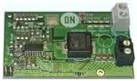
Figure 39. Typical Application Board Photos
ORDERING INFORMATION
Device
NCP1034DR2G
Package
Shipping†
SOIC−16
(Pb−Free)
2500 / Tape & Reel
†For information on tape and reel specifications, including part orientation and tape sizes, please refer to our Tape and Reel Packaging
Specifications Brochure, BRD8011/D.
www.onsemi.com
24
�MECHANICAL CASE OUTLINE
PACKAGE DIMENSIONS
SOIC−16
CASE 751B−05
ISSUE K
DATE 29 DEC 2006
SCALE 1:1
−A−
16
NOTES:
1. DIMENSIONING AND TOLERANCING PER ANSI
Y14.5M, 1982.
2. CONTROLLING DIMENSION: MILLIMETER.
3. DIMENSIONS A AND B DO NOT INCLUDE MOLD
PROTRUSION.
4. MAXIMUM MOLD PROTRUSION 0.15 (0.006) PER SIDE.
5. DIMENSION D DOES NOT INCLUDE DAMBAR
PROTRUSION. ALLOWABLE DAMBAR PROTRUSION
SHALL BE 0.127 (0.005) TOTAL IN EXCESS OF THE D
DIMENSION AT MAXIMUM MATERIAL CONDITION.
9
−B−
1
P
8 PL
0.25 (0.010)
8
M
B
S
G
R
K
F
X 45 _
C
−T−
SEATING
PLANE
J
M
D
DIM
A
B
C
D
F
G
J
K
M
P
R
MILLIMETERS
MIN
MAX
9.80
10.00
3.80
4.00
1.35
1.75
0.35
0.49
0.40
1.25
1.27 BSC
0.19
0.25
0.10
0.25
0_
7_
5.80
6.20
0.25
0.50
INCHES
MIN
MAX
0.386
0.393
0.150
0.157
0.054
0.068
0.014
0.019
0.016
0.049
0.050 BSC
0.008
0.009
0.004
0.009
0_
7_
0.229
0.244
0.010
0.019
16 PL
0.25 (0.010)
M
T B
S
A
S
STYLE 1:
PIN 1.
2.
3.
4.
5.
6.
7.
8.
9.
10.
11.
12.
13.
14.
15.
16.
COLLECTOR
BASE
EMITTER
NO CONNECTION
EMITTER
BASE
COLLECTOR
COLLECTOR
BASE
EMITTER
NO CONNECTION
EMITTER
BASE
COLLECTOR
EMITTER
COLLECTOR
STYLE 2:
PIN 1.
2.
3.
4.
5.
6.
7.
8.
9.
10.
11.
12.
13.
14.
15.
16.
CATHODE
ANODE
NO CONNECTION
CATHODE
CATHODE
NO CONNECTION
ANODE
CATHODE
CATHODE
ANODE
NO CONNECTION
CATHODE
CATHODE
NO CONNECTION
ANODE
CATHODE
STYLE 3:
PIN 1.
2.
3.
4.
5.
6.
7.
8.
9.
10.
11.
12.
13.
14.
15.
16.
COLLECTOR, DYE #1
BASE, #1
EMITTER, #1
COLLECTOR, #1
COLLECTOR, #2
BASE, #2
EMITTER, #2
COLLECTOR, #2
COLLECTOR, #3
BASE, #3
EMITTER, #3
COLLECTOR, #3
COLLECTOR, #4
BASE, #4
EMITTER, #4
COLLECTOR, #4
STYLE 4:
PIN 1.
2.
3.
4.
5.
6.
7.
8.
9.
10.
11.
12.
13.
14.
15.
16.
STYLE 5:
PIN 1.
2.
3.
4.
5.
6.
7.
8.
9.
10.
11.
12.
13.
14.
15.
16.
DRAIN, DYE #1
DRAIN, #1
DRAIN, #2
DRAIN, #2
DRAIN, #3
DRAIN, #3
DRAIN, #4
DRAIN, #4
GATE, #4
SOURCE, #4
GATE, #3
SOURCE, #3
GATE, #2
SOURCE, #2
GATE, #1
SOURCE, #1
STYLE 6:
PIN 1.
2.
3.
4.
5.
6.
7.
8.
9.
10.
11.
12.
13.
14.
15.
16.
CATHODE
CATHODE
CATHODE
CATHODE
CATHODE
CATHODE
CATHODE
CATHODE
ANODE
ANODE
ANODE
ANODE
ANODE
ANODE
ANODE
ANODE
STYLE 7:
PIN 1.
2.
3.
4.
5.
6.
7.
8.
9.
10.
11.
12.
13.
14.
15.
16.
SOURCE N‐CH
COMMON DRAIN (OUTPUT)
COMMON DRAIN (OUTPUT)
GATE P‐CH
COMMON DRAIN (OUTPUT)
COMMON DRAIN (OUTPUT)
COMMON DRAIN (OUTPUT)
SOURCE P‐CH
SOURCE P‐CH
COMMON DRAIN (OUTPUT)
COMMON DRAIN (OUTPUT)
COMMON DRAIN (OUTPUT)
GATE N‐CH
COMMON DRAIN (OUTPUT)
COMMON DRAIN (OUTPUT)
SOURCE N‐CH
COLLECTOR, DYE #1
COLLECTOR, #1
COLLECTOR, #2
COLLECTOR, #2
COLLECTOR, #3
COLLECTOR, #3
COLLECTOR, #4
COLLECTOR, #4
BASE, #4
EMITTER, #4
BASE, #3
EMITTER, #3
BASE, #2
EMITTER, #2
BASE, #1
EMITTER, #1
SOLDERING FOOTPRINT
8X
6.40
16X
1
1.12
16
16X
0.58
1.27
PITCH
8
9
DIMENSIONS: MILLIMETERS
DOCUMENT NUMBER:
DESCRIPTION:
98ASB42566B
SOIC−16
Electronic versions are uncontrolled except when accessed directly from the Document Repository.
Printed versions are uncontrolled except when stamped “CONTROLLED COPY” in red.
PAGE 1 OF 1
ON Semiconductor and
are trademarks of Semiconductor Components Industries, LLC dba ON Semiconductor or its subsidiaries in the United States and/or other countries.
ON Semiconductor reserves the right to make changes without further notice to any products herein. ON Semiconductor makes no warranty, representation or guarantee regarding
the suitability of its products for any particular purpose, nor does ON Semiconductor assume any liability arising out of the application or use of any product or circuit, and specifically
disclaims any and all liability, including without limitation special, consequential or incidental damages. ON Semiconductor does not convey any license under its patent rights nor the
rights of others.
© Semiconductor Components Industries, LLC, 2019
www.onsemi.com
�onsemi,
, and other names, marks, and brands are registered and/or common law trademarks of Semiconductor Components Industries, LLC dba “onsemi” or its affiliates
and/or subsidiaries in the United States and/or other countries. onsemi owns the rights to a number of patents, trademarks, copyrights, trade secrets, and other intellectual property.
A listing of onsemi’s product/patent coverage may be accessed at www.onsemi.com/site/pdf/Patent−Marking.pdf. onsemi reserves the right to make changes at any time to any
products or information herein, without notice. The information herein is provided “as−is” and onsemi makes no warranty, representation or guarantee regarding the accuracy of the
information, product features, availability, functionality, or suitability of its products for any particular purpose, nor does onsemi assume any liability arising out of the application or use
of any product or circuit, and specifically disclaims any and all liability, including without limitation special, consequential or incidental damages. Buyer is responsible for its products
and applications using onsemi products, including compliance with all laws, regulations and safety requirements or standards, regardless of any support or applications information
provided by onsemi. “Typical” parameters which may be provided in onsemi data sheets and/or specifications can and do vary in different applications and actual performance may
vary over time. All operating parameters, including “Typicals” must be validated for each customer application by customer’s technical experts. onsemi does not convey any license
under any of its intellectual property rights nor the rights of others. onsemi products are not designed, intended, or authorized for use as a critical component in life support systems
or any FDA Class 3 medical devices or medical devices with a same or similar classification in a foreign jurisdiction or any devices intended for implantation in the human body. Should
Buyer purchase or use onsemi products for any such unintended or unauthorized application, Buyer shall indemnify and hold onsemi and its officers, employees, subsidiaries, affiliates,
and distributors harmless against all claims, costs, damages, and expenses, and reasonable attorney fees arising out of, directly or indirectly, any claim of personal injury or death
associated with such unintended or unauthorized use, even if such claim alleges that onsemi was negligent regarding the design or manufacture of the part. onsemi is an Equal
Opportunity/Affirmative Action Employer. This literature is subject to all applicable copyright laws and is not for resale in any manner.
PUBLICATION ORDERING INFORMATION
LITERATURE FULFILLMENT:
Email Requests to: orderlit@onsemi.com
onsemi Website: www.onsemi.com
◊
TECHNICAL SUPPORT
North American Technical Support:
Voice Mail: 1 800−282−9855 Toll Free USA/Canada
Phone: 011 421 33 790 2910
Europe, Middle East and Africa Technical Support:
Phone: 00421 33 790 2910
For additional information, please contact your local Sales Representative
�


 工商网监
湘ICP备2023018690号
工商网监
湘ICP备2023018690号
