NCP1230GEVB
NCP1230 90 Watt, Universal
Input Adapter Power Supply
Evaluation Board User's
Manual
http://onsemi.com
EVAL BOARD USER’S MANUAL
General Description
Design Specification
The NCP1230 implements a standard current mode
control architecture. It’s an ideal candidate for applications
where a low parts count is a key parameter, particularly in
low cost adapter power supplies. The NCP1230 combines a
low standby power mode with an event management scheme
that will disable a PFC circuit during Standby, thus reducing
the no load power consumption. The 90 W Evaluation
Board demonstrates the wide range of features found on the
NCP1230 controller.
The NCP1230 has a PFC_Vcc output pin which provides
Vcc power for a PFC controller, or other circuitry. The
PFC_Vcc pin is enabled when the output of the power
supply is up and in regulation. In the event that there is an
output fault, the PFC_Vcc pin is turned off, disabling the
PFC controller, reducing the stress on the PFC
semiconductors.
In addition to excellent no load power consumption, the
NCP1230 provides an internal latching function that can be
used for over voltage protection by pulling the CS pin above
3.0 V.
This Demo Board is configured as a two stage adapter
power supply. The first stage operates off of the universal
input, 85−265 Vac, 50−60 Hz, using the MC33260 Critical
Conduction Mode controller, in the Boost Follower mode.
The output voltage from the Boost Follower (when Vin is
85 Vac) is 200 V and as the input line increases to 230 Vac
the output of the Boost Follower will ramp up to 400 Vdc.
The second stage of the power supply features the NCP1230
driving a flyback power stage. The output of the second
stage is 19 Vdc capable of 90 W of output power. It is fully
self−contained and includes a bias supply that operates off
of the Auxiliary winding of the transformer.
Table 1. EVALUATION BOARD SPECIFICATIONS
Current−Mode Control
Lossless Startup Circuit
Operation Over the Universal Input Range
Direct Connection to PFC Controller
Low Standby
Overvoltage Protection
Symbol
Min
Max
Input
Vac
85
265
Frequency
Hz
47
63
Vo
Vdc
18.6
19.38
Io
Adc
−
4.74
Output Power
W
−
90
efficiency
h
80
−
Standby Power
Vin 230 Vac
mW
−
150
Pin Short Circuit Load
Vin 230 Vac
mW
Pin with 0.5 W Load
Vin 230 Vac
mW
Features
•
•
•
•
•
•
Requirement
100
−
0.8
PFC
The MC33260 is configured as a Boost Follower
operating from the universal input line. The PFC section was
designed to provide approximately 116 W of power.
Ipk +
August, 2012 − Rev. 1
Vac
2 · Ǹ2 · 116
Ipk +
+ 3.86 A
85
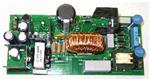
Figure 1. Evaluation Board Photo
© Semiconductor Components Industries, LLC, 2012
2 · Ǹ2 · Pin max
1
Publication Order Number:
EVBUM2131/D
�NCP1230GEVB
Vdc bus = 200 Vdc input with Vin 85 Vac
Efficiency = 0.80
Freq = 65 kHz
Vo = 19 V
Vf = 0.7
Po = 90 W
The MC33260 is a Critical Conduction Mode controller;
as a result the switching frequency is a function of the boost
inductor and the timing capacitor. In this application the
minimum operating frequency is 30 kHz.
Lp +
Lp +
ǒ
Vo
Ǹ2
2 · Tp
Ǔ
* Vac · (Vac)2
Vo · Vac · Ipk
ǒ
2 · 33.33
200
Ǹ2
Ǔ
* 85 · (85)2
200 · 85 · 3.86
90
Pin + Po
h + 0.8 + 112.5 W
Iavg + Pin + 112.5 + 0.566
200
Vin
+ 414 mH
The value used is 400 mH.
Where:
Tp +
Lp +
1
+ 1 + 33.33 m sec
30
Freq min
Lp +
Vomin = 200 Vdc (@ 85 Vac input)
Vac = 85 Vac
The oscillator timing capacitor is calculated by the
following formula:
CT +
ǒ
2 · Pin
ǒ
2 · Iavg
D max
Ǔ · Freq
2 · 112.5
+ 432 mH
265
2 · 0.566
0.4
Ǔ
In this application the primary inductance used is 220 mH.
This takes into consideration the transformer tolerances, and
to minimize the transformer size. Once the primary
inductance has been calculated, the next step is to determine
the peak primary current.
4 Vo2 Kosc Lp Pin
* Cint
Ro2 Vpk2
Pin + 1 · Ipk2 · Lp · f
2
4 · 2002 · 6400 · 400 · 116
CT +
* 15 + 809 pF
22 · 1202
Ipk +
Where:
Kosc = 6400
Ro = 2.0 MW (feedback resistor)
The CT value used is 820 pF
Refer to the ON Semiconductor website for Application
Note AND8123/D for additional MC33260 application
information, and the Excel based development tool
DDTMC33260/D.
Ipk +
Ǹ
Pin · 2
Lp · f
Ǹ
2 · 112.5
+ 3.97 Apk
220 · 65
The following calculations are used to verify that the
current will be Discontinuous under all operating
conditions.
Tp + Ton ) Toff u 1
freq
Startup Circuit Description
The High Voltage pin (pin 8) of the NCP1230 controller
is connected directly to the high voltage DC bus. When the
input power is turned on, an internal current source is turned
on (typically 3.0 mA) charging up an external capacitor on
the Vcc pin. When the Vcc capacitor is above VCCoff, the
current source is turned off, and the controller delivers
output drive pulses to an external MOSFET, Q1. The
MOSFET, Q1, drives the primary of the transformer T1. The
transformer has two additional windings, the auxiliary
winding which provides power to the controller after the
power supply is running, and the secondary winding which
provided the 19 Vdc output power.
Ton +
Toff +
Tp +
Lp · Ipk
Vin
Ls · Iopk
Vo ) Vf
ǒLpVin· IpkǓ ) ǒLsVo·)IopkVf Ǔ
Where:
Ls +
Lp
n2
n is the transformer turns ratio 6.77
Transformer
Tp +
The transformer primary inductance was selected so the
current would be discontinuous under all operating
conditions. As a result the total switching period, Ton + Toff,
must be less than or equal to 1/frequency.
The following assumptions were used in the design
process:
Dmax = 0.4 Duty Cycle
220 · 3.97 4.8 · 27.22
)
+ 10 ms
200
19 ) 0.7
With a primary inductance value of 220 mH, Ton + Toff is
less than the controller switching period. An Excel
spreadsheet was designed using the above equation to help
calculate the correct primary inductance value; visit the
ON Semiconductor website for a copy of the spreadsheet.
http://onsemi.com
2
�NCP1230GEVB
One method for calculating the transformer turns ratio is
to minimize the voltage stress of the MOSFET (VDS) due to
the reflected output voltage.
in the output capacitor(s). As a result you may be required
to use multiple capacitors in parallel to handle the ripple
current.
VDSmax + Vinmax ) n · (Vo ) Vf) ) Vspike
I_cap_ripple + ǸIorms2 ) Io2
In this application an 800 V MOSFET was selected. The
goal, for safety purposes, is to limit VDSmax at high line
(including the Vspike) to 700 V. To limit the power
dissipation in the snubber clamp (refer to the section in the
Applications Note titled “Snubber”.) Vspike is clamped at
167 V.
n+
I_cap_ripple + Ǹ12.022 * 4.742 + 11.04 A
Ton +
Co +
VDSmax * Vinmax * Vspike
Vo ) Vf
Co +
12.02 @ (15.38−9.23)
+ 1, 478 mF
0.05
In the 90 W Adapter design four 2200 mF (8800 mF total)
capacitors (C2, C3, C14, and C15) were required in parallel
to handle the ripple current.
A small LC filter has been added to the output of the power
supply to help reduce the output ripple. The cut−off
frequency for the filter is:
The NCP1230 requires that the controller Vcc be supplied
through an auxiliary winding on the transformer. The
nominal supply voltage for the controller is 13 Vdc.
Vaux(1−D max)
Vin · D max
fp +
13.7(1−0.4)
naux +
+ 0.128
200(0.4)
1
1
+
+ 15.6 kHz
2p ǸLC
2p Ǹ2.2 · 47
L1 = 2.2 mH
C8 = 47 mF
The supply voltage to the controller may be higher than
the calculated value because of the transformer leakage
inductance. The leakage inductance spike on the auxiliary
winding is averaged by the rectifier D2 and capacitor C5.
Because of this, an 18 V Zener diode (D18 refer to the Demo
Board Schematic Figure 10) is connected from the Vcc pin
to ground. To limit the current into the Zener diode a 200 W
resistor is placed between C5 and the Vcc pin (R28).
ON Semiconductor recommends that the Vcc capacitor be
at least 47 mF to be sure that the Vcc supply voltage does not
drop below Vccmin (7.6 V typical) during standby power
mode and unusual fault conditions.
The transformer primary rms current is:
Irms + Ipk
Iorms @ (T−Ton)
Vripple
Where Vripple = 50 mV.
n + 700 * 400 * 167 + 6.77
19.7
naux +
1
0.4 + 1
0.4 + 6.15 m sec
65000
frequency
Output Rectifying Diode
The rectifying diode was selected based upon on the
peak inverse voltage and the diodes average forward current.
The peak inverse voltage across the secondary of the
transformer is:
PIV + Vin
n ) Vo
PIV + 400 ) 19 + 78 Vpk
6.77
The average current through the diode is:
Iavg + Po + 90 + 4.74 A
19
Vo
ǸDon
+ 3.97 Ǹ0.4 + 1.45 Arms
3
3
An MBR20100CT Schottky diode was selected; it is rated
for a VRRM of 100 V, with an average forward current of
10 A.
The transformer secondary rms current is:
Ǹ1−D
3
+ 3.97 · 6.77 Ǹ0.6 + 12.02 Arms
3
Irms_sec + Ipk_prim · n
Power Switch
A MOSFET was selected as the power switching element.
Several factors were used in selecting the MOSFET; current,
voltage stress (VDS), and RDS(on).
The rms current through the primary of the transformer is
the same as the current in the MOSFET, which is 1.45 Arms.
The MOSFET selected is manufactured by Infineon, part
number SPP11N80C3. It is rated for 800 VDS and 11 Arms,
with an RDS(on) of 0.45 W.
The transformer for the Demo Board was manufactured
by Cooper Electronics Technologies (www.cooperET.com)
part number CTX22−16134. The designer should take
precautions that under startup conditions, the transformer
will not saturate at the low input ac line (85 Vac) and full load
conditions. The above calculation assumed that the adapter
was running and the PFC front end was enabled.
Output Filter
One of the disadvantages of a Flyback converter operating
in the Discontinuous mode is there is a large ripple current
http://onsemi.com
3
�NCP1230GEVB
Snubber
The maximum voltage across the MOSFET is:
Vpk + Vin max ) (Vo ) Vf)n
Vpk + 400 ) (19 ) 0.7) 6.77 + 534 V
This calculation neglects the voltage spike when the
MOSFET turns off due to the transformer leakage
inductance. The spike, due to the leakage inductance, must
be clamped to a level below the MOSFETs’ maximum VDS.
To clamp the voltage spike a resistive, capacitive, diode
clamp network was used to prevent the drain voltage from
rising above Vin + (Vo + Vf) n + Vclamp. The desired clamp
voltage is 700 V; this provides a safety margin of 100 V. The
first step is to calculate the snubber resistor.
2 · Vclamp · ǒVclamp * Vo · nǓ
Rclamp +
Rclamp +
Figure 2.
Current Sense Resistor Selection
le · Ipk2 · Freq
2 · 700 · ǒ700 * ǒ19.7 · 6.77ǓǓ
7 · 3.972 · 65
The input to the current sense amplifier is clamped to
1.0 V (typical). The current sense resistor should be
calculated at 125% of the full rated load to be sure that under
all operating conditions the power supply will be able to
deliver the full rated power.
+ 110 kW
Where:
Vo = the output voltage
Vf = the forward voltage drop across the output diode
n is the transformer turns ratio 6.77
Ie is the transformer turns ratio of 7 mH
The power dissipation in the clamp resistor is:
ǒ
ǒ
PRclamp + 0.5 · Ipk2 · le · Freq ·
PRclamp + 0.5 · 3.972 · 7 · 65 ·
Po + 90 · 1.25 + 112.5 W
Pin + Po + 112.5 + 140.63 W
0.80
eff
Ipk +
Ǔ
Ǔ
Vclamp
Vclamp * ǒVo · nǓ
700
700 * ǒ19.7 · 6.77Ǔ
Rs +
The snubber capacitor can be calculated from the
following equation. See Application Note AN1679/D for
details of how the snubber equations were derived.
C6 +
2 · 140.63
+ 4.43 Apk
220 · 65
1V
+ 1 + 0.23 W
4.43
Ipk
0.2 W was used.
To reduce the power dissipation in the sense resistor, two
0.4 W resistors were used in parallel.
+ 4.4 W
C6 +
Ǹ
Overvoltage Protection
The NCP1230 has a fast comparator which only monitors
the current sense pin during the power switch off time. If the
voltage on the current sense pin rises above 3.0 V (typical),
the NCP1230 will immediately stop the output drive pulses
and latch−off the controller. The NCP1230 will stay in the
Latch−Off mode until Vcc has dropped below 4.0 V.
This feature allows the user to implement several
protection functions, for example, Overvoltage or
Overtemperature Protection.
The Auxiliary winding of the Flyback transformer (T5)
can be used for overvoltage protection because the voltage
on the Auxiliary winding is proportional to the output
voltage.
Vclamp
Vripple · Freq · Rclamp
700
+ 0.005 mF
20 · 65 · 110
After the initial snubber was calculated, the snubber
values were tuned in the circuit to minimize ringing, and
minimize the power dissipation. As a result the final circuit
values are; Rclamp uses three 100 kW (33 kW equivalent),
2.0 W resistors used in parallel, and C6 is 0.01 mF, 1000 V.
Refer to Figure 2 for a scope waveform of the Drain to source
voltage at full load and high line.
http://onsemi.com
4
�NCP1230GEVB
Slope Compensation
To implement Overvoltage Protection (OVP), a PNP
transistor is used to bias up the current sense pin during the
NCP1230 controller off time (refer to Figure 3). The base of
the PNP transistor is driven by the NCP1230 drive output
(pin 5), if the Auxiliary winding voltage increases above the
Zener diode (D1) breakdown voltage, 13 V, current will
flow through Q3 biasing up the voltage on the current sense
pin. Using typical component values, if the voltage on the
Auxiliary winding reaches 16.5 V (3.5 V above the nominal
voltage) the NCP1230 will latch−off through the CS input
(pin 3).
A Flyback converter operating in continuous conduction
mode with a duty cycle greater than 50% requires slope
compensation. In this application the power supply will
always be operating in the discontinuous mode, so no slope
compensation is required.
The resistor R21 and capacitor C24 form a low pass filter
suppressing the leading edge of the current signal. Typically,
the leading edge of the current will have a large spike due to
the transformer leakage inductance. If the spike is not
filtered, it can prematurely turn off the MOSFET. The
NCP1230 does have a leading edge blanking circuit, but it
is a good design practice to add an external filter. The time
constant of the filter must be significantly higher than the
highest expected operating frequency, but low enough to
filter the spike.
OVPthreshold + Vz(D1) ) VceQ3 ) CSlatchoff
+ 13 V ) 0.5 V ) 3.0 V + 16.5 V
A 13 V Zener diode was selected to have the controller
Latch−Off prior to having Vcc reach its maximum allowable
voltage level, 18 V.
Output Control
Vaux
Feedback theory states that for the control loop to be stable
there must be at least 45° of phase margin when the loop gain
crosses cross zero dB. The following equations derive the
Flyback converter transfer function while operating in the
discontinuous continuous mode.
13 V
MMBT2907A/SOT
10 k
NCP1230
1
2
3
4
GTS HV
FB
CS VCC
GND DRV
1k
8
2
Po + Vo
Ro
6
5
Where:
Po is the maximum output power
Vo is the output voltage
Ro is the output resistance
Rsense
100 pF
P + 1 · Ipk2 · Lp · f
2
Where:
I is the peak primary current
Lp is the transformer primary inductance
F is the switching frequency of the controller
Figure 3. Overvoltage Protection Circuit
Overtemperature Protection
To implement Overtemperature Protection (OTP)
shutdown, the Zener diode can be replaced by an NTC (refer
to Figure 4), or an NTC can be placed in parallel with the
Zener diode to have OVP and OTP protection. When an
overtemperature condition occurs, the resistance of the NTC
will decrease, allowing current to flow through the PNP
transistor biasing up the Current Sense pin.
Vo2 + 1 · Ipk2 · Lp · f
2
Ro
Vo +
i
i + Ip · Rs + Vc
3
Vaux
Where:
Ip is the peak primary current
Rs is the current sense resistor
Vc is the control voltage
3, the feedback input voltage is divided down by a factor
of three
Combining equations the open loop gain is:
NTC
MMBT2907A/SOT
Q3
R26
10 k
NCP1230
1
2
3
4
GTS HV
FB
CS VCC
GND DRV
1k
C24
100 pF
ǸRo ·2f · Lp · n · d
8
6
5
Vo +
i
Rsense
ǸRo ·2Lp · f · n · d
i + Ipk @ Rs + Vc
3
Vc + 3 @ Rs @ Ipk
Figure 4. Overtemperature Protection Circuit
http://onsemi.com
5
�NCP1230GEVB
Vo +
Vc
ǸRo ·2Lp · f · n · d · Ipk · Rs · 3
The Standby power consumption is:
2
2
P + Vo + 19 + 6.3 mW
57400
Rtotal
With current mode control, there is pole associated with
the output capacitor(s) and the load resistors. In this
application there are four 2200 mF capacitors in parallel:
fp +
Standby power calculation:
P_R22 + I2 * R22 + 12 ma · 2 k + 2 mW
1
1
+
+ 9.3 Hz
pCoRo
p · 8800 · 3.9
P_TL431 + (Vo * V_R22 * Vopto) · 1 ma
+ 17 V · 1 ma + 17 mW
The secondary filter made up of L1 and C8 does not affect
the control loop because we are sensing the output voltage
before the LC network.
In addition to the pole, there is a zero associated with the
output capacitor(s) and the capacitors esr. The esr of each
capacitors is 0.022 W (from the data sheet).
fz +
1
1
+
2pCo · esr
6.28 · 8800 ·
0.022
4
Control Loop
Two methods were used to verify that the Demo Board
loop was stable, the results are shown below. The first
method was to use an Excel Spreadsheet (using the
previously derived equations) which can be down loaded
from the ON Semiconductor website (www.onsemi.com).
The results from the Excel Spreadsheet are shown below. At
full load and 200 Vdc (200 Vdc is the minimum voltage
being supplied from the PFC) the loop gain crosses zero dB
at approximately 1.2 kHz with approximately 100° of phase
margin.
The second method was to model the NCP1230 Demo
Board in PSPICE. The result can be seen in Figure 7.
Because parasitic elements can be added to the PSPICE
model, it was more accurate at high frequencies.
The results from the PSPICE model (at low frequencies)
shows similar results, the loop gain crosses zero dB at
approximately 1.2 kHz with about 90° of phase margin.
+ 3.3 kHz
A small 0.47 nF capacitor (C25) is connected from the
feedback pin to ground to reduce the switching noise on the
feedback pin. Care must be taken not to have too large a
capacitor, or a low frequency pole may be created in the
feedback loop.
Output Voltage Regulation
The output voltage regulation is achieved by using a
TL431 on the secondary side of the transformer. The output
voltage is sensed and divided down to the reference level of
the TL431 (2.5 V typical) by the resistive divider network
consisting of R4 and R10.
The TL431 requires a minimum of 1.0 mA of current for
regulation:
Ropto(R22) +
Loop Gain Plot
60
Vo * Vfopto
+ 19 * 1 + 18 k
1 mA
1 mA
40
20
GAIN IN dB
In this application R22 was changed to 1.0 kW to minimize
the stand by power consumption.
When the power supply is operating at no load, there may
not be sufficient current through the optocoupler LED, so a
resistor (R7) is placed in parallel. A 4.7 kW resistor was
selected.
The optocoupler gain is:
0
−20
−40
−60
−80
DVfb + Rfb · CTR + 20 · 1.0 + 20
1
Ropto
DVc
−100
10
dBgain + 20log20 + 26 dB
1000
10000
FREQUENCY IN Hz
100000
Figure 5. Excel Spreadsheet Loop Gain
CTR is the current transfer ratio of the opto and is
nominally 1.0, but over time the CTR will degrade so
analysis of the circuit with the CTR = 0.5 is recommended.
Rfb is the internal pull−up resistor of the NCP1230 and it
is a nominal 20 kW.
Standby Power
To minimize the standby power consumption, the output
voltage sense resistor divider network was select to consume
less than 10 mW.
Vref + Vo
100
Ǔ + 2.5 V
ǒR10R10
Ǔ + 19 ǒ7.47.4
) 50
) R4
http://onsemi.com
6
�NCP1230GEVB
Loop Phase Margin
180
180
140
100
100
PHASE
60
20
−20
0
−60
−100
−140
−100
10 Hz
−180
10
100
1000
FREQUENCY
10000
100000
100 Hz
DB(V(FB))
NCP1230 AV U7
+
−
Vin
200 Vdc
OUT
FB
GND
CTRL
IN
XFMR1
U6
R7
0.16
D4
MUR810
out1
L1
2.2 mH
FS = 65 k
L = 0.22 mH
RI = 0.20
LoL
1k
RATIO=0.1477
R3
0.022
R5
0.022
R8
0.022
R6
0.022
C4
C1
C5
C6
2200 mF 2200mF 2200mF 2200 mF
Vstim
FB
R11
1k
U10
R2
49.9 k
R1
4.7 k
C2
470 nF
MOC8101
C3
0.47 nF
100 kHz
Figure 7. SPICE Phase/Gain
CoL
1k
ACMAG=1
10 kHz
FREQUENCY
Figure 6. Excel Spreadsheet Phase Margin
NCP1230
averaged
1.0 kHz
P(V(FB))
U9
TL431
R4
7.4 k
Figure 8. AC Frequency Response SPICE Model
http://onsemi.com
7
Rload
3.9
C7
47 mF
�NCP1230GEVB
Evaluation Board Test Procedure
Figure 9. NCP1230GEVB Test Setup
8. Connect the Voltec Precision Power Analyzer as
shown in Figure 9.
9. Turn on the ac source to 115 Vac at 60 Hz and set
the electronic load to 90 W. (Only measure the
THD at full load).
10. Verify that the current Harmonics (THD) are less
than the maximum vales in Table 5.
11. Verify that the PF is greater than the minimum
values in Table 5.
12. Set the ac source output to 230 Vac at 60 Hz.
13. Verify that the current Harmonics (THD) are less
than the maximum vales in Table 5.
14. Verify that the PF is greater than the minimum
values in Table 5.
15. Set the ac source to 115 Vac, set the load to 0 Adc,
and measure the standby power, refer to Table 5
for the maximum acceptable input power.
16. Set the ac source to 230 Vac, and refer to Table 5
for the maximum input power.
Table 2. TEST EQUIPMENT
ac Source 85 − 265 Vac, 47 − 64 Hz
Variable Electronic Load
Digital Multimeter
Voltec Precision Power
Analyzer
Test Setup
1. Connect the ac source to the input terminals J4.
2. Connect a variable electronic load to the output
terminals J2, the PWB is marked +, for the
positive output, and − for the return.
3. Set the variable electronic load to 45 W.
4. Turn on the ac source and set it to 115 Vac at
60 Hz.
5. Verify that the NCP1230 provides 19 Vdc to the
load.
6. Vary the load and input voltage. Verify that the
output voltage is within the minimum and
maximum values as shown in Table 4.
7. To verify total harmonic distortion (THD) first,
shut off the ac power supply.
Table 3. EXPECTED VALUES FOR VARYING INPUT VOLTAGES AND LOADS
Vin
(Vac)
Vo (Vdc)
@ No Load
Vo (Vdc)
@ 45 W
Vo (Vdc)
@ 90 W
THD
(%)
PF
90 W
90
19.1
19.0
18.8
6.5
0.995
115
19.1
19.0
18.8
7.8
0.995
230
18.7
19.1
18.8
20
0.97
Table 3 shows typical values, the initial set point (19.0 Vdc may vary).
http://onsemi.com
8
�NCP1230GEVB
Table 4. REGULATION
Vin
(Vac)
Pinmax
(W)
Vomin
(Vdc)
Vomax
(Vdc)
IO
(Adc)
Po
(W)
Eff
(%)
90
115
18.7
19.1
4.85
90
80.0
115
114
18.7
19.1
4.85
90
80.0
230
112
18.7
19.1
4.85
90
81.0
Table 5. STAND-BY POWER
Table 6. POWER FACTOR AND THD
Vin
(Vac)
Pinmax
(mW)
Vin
(Vac)
PFmin
(W)
THDmax
(%)
PO
(W)
115
150
90
0.990
8.0
90
230
200
115
0.990
9.0
90
230
0.96
21.0
90
http://onsemi.com
9
�J4
1
2
1
2
C11
0.1
mF
F1
L2
2
L3
2
100 mH
1
100 mH
1
C27
0.22
mF
L5
4
3
4.5 mH
2
1
C22
0.47
mF
http://onsemi.com
10
R16
1.3
D10
D11
1N5406 1N5406
D8
D9
1N5406 1N5406
R5
1.3
R6
1.3
8.06k
R17
C17
0.1 mF
C18
680 pF
SYNC VCC
GND DRV
4
5
6
7
8
D17
18 V
FB
CS
3
VC
OSC
2
U1
MC33260
1
400 mH
L4
C19
0.1 mF
4.7
R27
C12
0.68 mF
C13
470 pF
SPP07N60C3
Q2
MUR460
D12
C23
150 mF
+
R20
1M
GND
PFC_Vcc
R19
1M
+VDC
NCP1230GEVB
Figure 10. NCP1230 Demo Board Schematic − PFC section
�PFC_Vcc
+VDC
11
Figure 11. DC−DC section
http://onsemi.com
100pF
C24
NCP1230
CS VCC
GND DRV
5
6
C7
47 mF
R2
R18
C1
0.1 mF
R21
1k
2
+
3
4
4
5
7
6
U13
2
1
0.4 0.4
C10
2.2nF
D19
C2
2200
mF
U12
TL431
R7
4.7k
1k
R22
MBR20100CT
R1 R3
T5
100 nF
C20
C15
2200
mF
+
SFH615AA−X007
D18
18 V
Q1
SPP11N80C3
R13
20
D2
BAL19LT1
C5
100 mF
D16
BAL19LT1
200
R28
R29
100k 100k
D4 220 mH
3
MUR160
100k
+
C25
1.0 nF
R26
10k
4
8
D13
1N4006
D15
1N4006
C6
0.01 mF
+
3
MMBT2907A/SOT
Q3
1
GTS HV
2
FB
D1
13 V
R25
200
R24
0
C14
2200
mF
C3
2200
mF
R10
7.4k
2.2 mH
R4
49.9k
L1
C8
47mF
1
2
J2
NCP1230GEVB
+
+
+
�NCP1230GEVB
Table 7. Voltage Regulation and Efficiency
Vin
(Vac)
Pin
(W)
Vo
(Vdc)
Io
(Adc)
Po
(W)
Eff
(%)
85
54.50
19.02
2.36
45
82.57
115
54.40
19.03
2.36
45
82.72
230
53.21
19.06
2.36
45
84.54
265
53.1
19.06
2.36
45
84.71
85
112.00
18.82
4.77
90
80.36
115
110.84
18.88
4.77
90
81.2
230
109.42
18.88
4.77
90
82.25
265
109.01
18.89
4.77
90
82.56
Table 8. Power Factor and Distortion
Vin
(Vac)
Pin
(W)
PF
THD
(%)
Vo
(Vdc)
Po
(W)
85
112.00
0.996
6.5
18.82
90
115
110.84
0.996
7.7
18.88
90
230
109.42
0.972
19.01
18.88
90
265
109.01
0.965
23.0
18.89
90
Table 9. Standby Power
Test
Condition
(Vac input)
Requirement Pin
(mW)
Pin Measured
(mW)
Standby Power
230
150
120
Pin Short Circuit
230
100
100
Pin with 0.5 W Load
230
800
600
Table 10. Vendor Contact List
ON Semiconductor
www.onsemi.com 1−800−282−9855
TDK
www.component.tdk.com 1−847−803−6100
Infineon
www.infineon.com
Coilcraft
www.coilcraft.com
Vishay
www.vishay.com
Coiltronics
www.cooperet.com 1−888−414−2645
Bussman (Cooper Ind.)
www.cooperet.com 1−888−414−2645
Panasonic
www.eddieray.com/panasonic.com
Weidmuller
www.weidmuller.com
Keystone
www.keyelco.com 1−800−221−5510
HH Smith
www.hhsmith.com 1−888−847−6484
Aavid Thermalloy
www.aavid.com
http://onsemi.com
12
�NCP1230GEVB
Table 11. NCP1230 EVALUATION BOARD BILL OF MATERIALS
Designator
QTY
Description
U9
1
U2
Manufacturer
Manufacturer Part
Number
Substitution
Allowed
RoHS
Compliant
SOIC 8
ON
Semiconductor
NCP1230D65R2G
No
Yes
SOIC 8
ON
Semiconductor
MC33260DG
No
Yes
NA
SOIC 8
ON
Semiconductor
TL431ACDG
No
Yes
Value
Tolerance
Footprint
Flyback Controller
18 V, 0.5 A
NA
1
PFC controller
16 V, 0.6 A
NA
U12
1
Programable
reference
2.5 V
U4
1
Optocoupler
70 V, 50 Ma
NA
UL1577
Vishay
SFH615A-3
Yes
Yes
C1,
C19
2
Ceramic chip
capacitor
0.1 uF, 50 V
10%
0603
Vishay
VJ0603Y104KXAA
Yes
Yes
C2,
C3,
C14,
C15
4
Electorlytic
Capacitor
2200 uF, 25 V
20%
16.0 mm
x 25.0 mm
Vishay
EKB00JG422F00
Yes
Yes
C5
1
Electorlytic
Capacitor
100 uF, 35 V
20%
6.3 mm x
11.0 mm
Vishay
EKB00BA310F00
Yes
Yes
C6
1
Cap, Ceramic
0.01uF, 1000V
10%
Disc
Vishay
562RZ5UBA102E103M
Yes
Yes
C7, C8
2
Cap. Aluminum
Elec
47 uF, 25 V
20%
5.0 mm x
11.0 mm
Vishay
EKB00AA247F00
Yes
Yes
C10
1
Capacitor, Y2
class
2.2 nF, 250 V
20%
5.3 mm x
10.3 mm
Vishay
F1710-222-1000
Yes
Yes
C11,
C17
2
Capacitor, X2
class
0.1 uF, 300 V
10%
8.3 mm x
17.8 mm
Vishay
F1772-410-3000
Yes
Yes
C12
1
Ceramic chip
capacitor
0.068 uF, 50 V
10%
0603
Vishay
VJ0603Y683KXAA
Yes
Yes
C13
1
Ceramic chip
capacitor
470 pF, 50 V
10%
0603
Vishay
VJ0603471KXAA
Yes
Yes
C18
1
Ceramic chip
capacitor
680 pF, 50V
10%
0603
Vishay
VJ0603Y681KXAA
Yes
Yes
C20
1
Cap. Ceramic,
chip
0.047 uF, 16 V
10%
0805
Vishay
VJ0805Y473KXJA
Yes
Yes
Vishay
F1772-447-3000
Yes
Yes
C22
1
Capaitor, X2 class
0.47 uF, 300 V
10%
13.0 mm x
31.3 mm
C23
1
Cap. Aluminum
150uF, 450Vdc
20%
25mm x
40mm
Panasonic
ECOS2WP151CA
Yes
Yes
C24
1
Ceramic chip
capacitor
100 pF, 50 V
10%
0805
Vishay
VJ0805100KXAA
Yes
Yes
C25
1
Ceramic chip
capacitor
1.0 nF, 50 V
10%
0805
Vishay
VJ0805Y102KXAA
Yes
Yes
C27
1
Capacitor, X2
class
0.22 uF, 300 V
10%
10.3 mm
x 26.3 mm
Vishay
F1772-422-3000
Yes
Yes
D1
1
Zener Diode, SM
13 V, 0.3 W
NA
SOT-23
Vishay
AZ23C13
Yes
Yes
BAS19LT1G
No
Yes
D2,
D16
2
Diode, signal
75V, 100ma
NA
SOT-23
ON
Semiconductor
D4
1
Diode, ultra fast
600 V, 1 A
NA
DO41
ON
Semiconductor
MUR160
No
Yes
D8,
D9,
D10,
D11
4
Diode, rectifier
1000 V, 3 A
NA
DO201AD
ON
Semiconductor
1N5408G
No
Yes
D12
1
Diode, ultra-fast
600 V, 4 A
NA
DO201AD
ON
Semiconductor
MUR460
No
Yes
1N4006
No
Yes
AZ23C18
Yes
Yes
D13,
D15
2
Diode, rectifier
800 V, 1 A
NA
DO41
ON
Semiconductor
D17,
D18
2
Zener Diode, SM
18 V, 0.3 W
NA
SOT-23
Vishay
http://onsemi.com
13
�NCP1230GEVB
Table 11. NCP1230 EVALUATION BOARD BILL OF MATERIALS
Manufacturer
Manufacturer Part
Number
Substitution
Allowed
RoHS
Compliant
ON
Semiconductor
MBR20100CTG
No
Yes
10mm x
2.5mm
Bussman
1025TD2
Yes
Yes
NA
5.08 mm
Weidmuller
171602
Yes
Yes
2.2 uH, 7.5 A
10%
13 mm x
9 mm
Coilcraft
DO3316P-222ML
Yes
Yes
Inductor
100 uH, 2.5 A
10%
1315
TDK
TSL1315-101K2R5
Yes
Yes
1
PFC Indcutor
400 uH, 5 A
20%
NA
Cooper
Electronics
CTX22-16816
Yes
Yes
L5
1
Common Mode
Inductor
508 uH, 3 A
30%
NA
Coilcraft
E3506-AL
Yes
Yes
Q1
1
MOSFET 0.8 W
800 V, 11 A
NA
TO220-31
Infineon
SPP11N80C3
Yes
Yes
Q2
1
MOSFET 0.8 W
650 V, 7.3 A
NA
TO220-31
Infineon
SPP07N60C3
Yes
Yes
Q3
1
Bipolar transistor
60 V, 0.6 A
NA
SOT-23
ON
Semiconductor
MMBT2907ALT1G
No
Yes
R1, R3
2
Resistor
0.4 W, 1 W
1%
2512
Vishay
WSL2512R4000FEA
Yes
Yes
R2,
R18,
R29
3
Resistor
100k, 3W
5%
14.10 mm
x 4.57 mm
Vishay
CPF3100k00JNE14
Yes
Yes
R4
1
Resistor
49.9 kW, 1/8 W
1%
0805
Vishay
CRCW08054992FNEA
Yes
Yes
R5,
R6,
R16
3
Resistor
1.3 W, 1 W
1%
2512
Vishay
CRCW25121R30FNEA
Yes
Yes
R7
1
Resistor
4.7 kW, 1/8 W
5%
0805
Vishay
CRCW8054700RJNEA
Yes
Yes
R10
1
Resistor
7.42 kW, 1/8 W
1%
0805
Vishay
CRCW08057421FNEA
Yes
Yes
R13
1
Resistor
20 W, 1/4 W
5%
1206
Vishay
CRCW120620R0JNEA
Yes
Yes
R17
1
Resistor
8.06 kW, 1/8 W
1%
0805
Vishay
CRCW08058K06FKEA
Yes
Yes
R19,
R20
2
Resistor
1 MW, 1/8 W
1%
6.10 mm
x 2.29 mm
Vishay
CMF551004FKEK
Yes
Yes
R21,
R22
2
Resistor
1 kW, 1/4 W
1%
1206
Vishay
CRCW12061K00FKEA
Yes
Yes
R24
1
Jumper, 22 AWG
NA
NA
NA
Any
NA
Yes
Yes
R25
1
Resistor
200 W, 1/4 W
5%
1206
Vishay
CRCW1206200RJNEA
Yes
Yes
R26
1
Resistor
10 kW, 1/4 W
5%
1206
Vishay
CRCW120610K0JNEA
Yes
Yes
R27
1
Resistor
4.7 W, 1/4 W
5%
1206
Vishay
CRCW12064R7JNEA
Yes
Yes
R28
1
Resistor
200 W, 1/4 W
5%
1206
Vishay
CRCW1206200RJNEA
Yes
Yes
T1
1
Flyback
Transformer
220 uH, 3.3
Apk
NA
NA
Cooper
Electronics
CTX22-16134
Yes
Yes
H1
1
Shoulder Washer
NA
NA
#4 x
0.031”
Keystone
3049
Yes
Yes
Keystone
4672
Yes
Yes
Aavid
590302B03600
Yes
Yes
Value
Tolerance
Footprint
Diode, schottky
100 V, 20 A
NA
TO220AB
1
Brick Fuse
250 Vac, 2 A
NA
J2, J4
2
PCB Connector
10 A, 300 V
L1
1
Inductor
L2, L3
2
L4
Designator
QTY
Description
D19
1
F1
H2
1
Insulator
NA
NA
0.86 ” x
0.52 ”
H3,
H4, H5
3
Heatsink
NA
NA
TO-220
http://onsemi.com
14
�onsemi,
, and other names, marks, and brands are registered and/or common law trademarks of Semiconductor Components Industries, LLC dba “onsemi” or its affiliates
and/or subsidiaries in the United States and/or other countries. onsemi owns the rights to a number of patents, trademarks, copyrights, trade secrets, and other intellectual property. A
listing of onsemi’s product/patent coverage may be accessed at www.onsemi.com/site/pdf/Patent−Marking.pdf. onsemi is an Equal Opportunity/Affirmative Action Employer. This
literature is subject to all applicable copyright laws and is not for resale in any manner.
The evaluation board/kit (research and development board/kit) (hereinafter the “board”) is not a finished product and is not available for sale to consumers. The board is only intended
for research, development, demonstration and evaluation purposes and will only be used in laboratory/development areas by persons with an engineering/technical training and familiar
with the risks associated with handling electrical/mechanical components, systems and subsystems. This person assumes full responsibility/liability for proper and safe handling. Any
other use, resale or redistribution for any other purpose is strictly prohibited.
THE BOARD IS PROVIDED BY ONSEMI TO YOU “AS IS” AND WITHOUT ANY REPRESENTATIONS OR WARRANTIES WHATSOEVER. WITHOUT LIMITING THE FOREGOING,
ONSEMI (AND ITS LICENSORS/SUPPLIERS) HEREBY DISCLAIMS ANY AND ALL REPRESENTATIONS AND WARRANTIES IN RELATION TO THE BOARD, ANY
MODIFICATIONS, OR THIS AGREEMENT, WHETHER EXPRESS, IMPLIED, STATUTORY OR OTHERWISE, INCLUDING WITHOUT LIMITATION ANY AND ALL
REPRESENTATIONS AND WARRANTIES OF MERCHANTABILITY, FITNESS FOR A PARTICULAR PURPOSE, TITLE, NON−INFRINGEMENT, AND THOSE ARISING FROM A
COURSE OF DEALING, TRADE USAGE, TRADE CUSTOM OR TRADE PRACTICE.
onsemi reserves the right to make changes without further notice to any board.
You are responsible for determining whether the board will be suitable for your intended use or application or will achieve your intended results. Prior to using or distributing any systems
that have been evaluated, designed or tested using the board, you agree to test and validate your design to confirm the functionality for your application. Any technical, applications or
design information or advice, quality characterization, reliability data or other services provided by onsemi shall not constitute any representation or warranty by onsemi, and no additional
obligations or liabilities shall arise from onsemi having provided such information or services.
onsemi products including the boards are not designed, intended, or authorized for use in life support systems, or any FDA Class 3 medical devices or medical devices with a similar
or equivalent classification in a foreign jurisdiction, or any devices intended for implantation in the human body. You agree to indemnify, defend and hold harmless onsemi, its directors,
officers, employees, representatives, agents, subsidiaries, affiliates, distributors, and assigns, against any and all liabilities, losses, costs, damages, judgments, and expenses, arising
out of any claim, demand, investigation, lawsuit, regulatory action or cause of action arising out of or associated with any unauthorized use, even if such claim alleges that onsemi was
negligent regarding the design or manufacture of any products and/or the board.
This evaluation board/kit does not fall within the scope of the European Union directives regarding electromagnetic compatibility, restricted substances (RoHS), recycling (WEEE), FCC,
CE or UL, and may not meet the technical requirements of these or other related directives.
FCC WARNING – This evaluation board/kit is intended for use for engineering development, demonstration, or evaluation purposes only and is not considered by onsemi to be a finished
end product fit for general consumer use. It may generate, use, or radiate radio frequency energy and has not been tested for compliance with the limits of computing devices pursuant
to part 15 of FCC rules, which are designed to provide reasonable protection against radio frequency interference. Operation of this equipment may cause interference with radio
communications, in which case the user shall be responsible, at its expense, to take whatever measures may be required to correct this interference.
onsemi does not convey any license under its patent rights nor the rights of others.
LIMITATIONS OF LIABILITY: onsemi shall not be liable for any special, consequential, incidental, indirect or punitive damages, including, but not limited to the costs of requalification,
delay, loss of profits or goodwill, arising out of or in connection with the board, even if onsemi is advised of the possibility of such damages. In no event shall onsemi’s aggregate liability
from any obligation arising out of or in connection with the board, under any theory of liability, exceed the purchase price paid for the board, if any.
The board is provided to you subject to the license and other terms per onsemi’s standard terms and conditions of sale. For more information and documentation, please visit
www.onsemi.com.
PUBLICATION ORDERING INFORMATION
LITERATURE FULFILLMENT:
Email Requests to: orderlit@onsemi.com
onsemi Website: www.onsemi.com
◊
TECHNICAL SUPPORT
North American Technical Support:
Voice Mail: 1 800−282−9855 Toll Free USA/Canada
Phone: 011 421 33 790 2910
www.onsemi.com
1
Europe, Middle East and Africa Technical Support:
Phone: 00421 33 790 2910
For additional information, please contact your local Sales Representative
�


 工商网监
湘ICP备2023018690号
工商网监
湘ICP备2023018690号
