NCP1406, NCV1406
Boost Converter - PFM,
DC-DC
25 V, 25 mA
The NCP1406 is a monolithic step−up DC−DC converter operating
in a Pulse Frequency Modulation (PFM) scheme with constant peak
current control. It integrates a 0.8 A, 0.7 W internal power switch and
sensing resistor to monitor inductor current. This control scheme
maintains high efficiencies over the entire load current range. The
wide input voltage range, from 1.4V to 5.5 V, enables the user to
operate the device from a Li−Ion battery or a two−cell Alkaline
NiMH. Its ability to boost voltages up to 25 V, and to provide 1 W
output power, makes the NCP1406 the perfect solution for biasing
small and large OLED panels. This device also makes a perfect
solution for biasing a great number of white LEDs in series. A Chip
Enable pin allows the user to control the device to extend the battery
life during standby, and can be pulse−width modulated for white
LED applications. The versatility of the NCP1406 allows it to be
configured not only as a step−up converter, but also as an inverter and
as a step−down converter. This solution is proposed in a
space−saving TSOP−5 package.
http://onsemi.com
MARKING
DIAGRAM
5
5
1
TSOP−5/SOT23−5/SC59−5
SN SUFFIX
CASE 483
PIN CONNECTIONS
87% Efficiency at VOUT = 25 V, IOUT = 25 mA, VIN = 5 V
Adjustable Output Voltage up to 25 V
0.8 A, 26 V Internal Power Switch
Operating Input Voltage from 1.4 V to 5.5 V
Low Startup Voltage of 1.8 V Typical at No Load
Low Operating Current of 15 mA (Not Switching)
Low Shutdown Current of 0.3 mA
Operating Switching Frequency up to 1 MHz
Output Voltage Soft−Start
Thermal Shutdown Protection
These are Pb−Free Devices
NCV Prefix for Automotive and Other Applications Requiring
Unique Site and Control Change Requirements; AEC−Q100
Qualified and PPAP Capable
LCD Bias Supplies
Small and Large OLED Display Drivers
White LED Driver for Backlight Displays
Personal Digital Assistants (PDA)
Portable Applications:
♦ Cell Phones, Digital Cameras
♦ PDAs, Games, and Portable Video Players
© Semiconductor Components Industries, LLC, 2012
August, 2019 − Rev. 6
CE
1
FB
2
VDD
3
5
LX
4 GND
(Top View)
ORDERING INFORMATION
Device
Package
Shipping†
NCP1406SNT1G
TSOP−5
(Pb−Free)
3000 Tape & Reel
NCV1406SNT1G
TSOP−5
(Pb−Free)
3000 Tape & Reel
†For information on tape and reel specifications,
including part orientation and tape sizes, please
refer to our Tape and Reel Packaging Specification
Brochure, BRD8011/D.
Typical Applications
•
•
•
•
•
1
DAM
= Device Marking − NCP1406
AET
= Device Marking − NCV1406
A
= Assembly Location
Y
= Year
W
= Work Week
G
= Pb−Free Package
(Note: Microdot may be in either location)
Features
•
•
•
•
•
•
•
•
•
•
•
•
XXX AYW G
G
1
Publication Order Number:
NCP1406/D
�NCP1406, NCV1406
100
VOUT
15 V
D
SUMIDA
CR43−8R2MC
VDD
Enable
CE
OLED
CIN
10 mF
CC
68 pF
R2
1.3 mW
LX
FB
GND
R1
110 kW
5.0 V
4.2 V
3.7 V
90
EFFICIENCY (%)
L
8.2 mH
VIN
2.4 V
3.0 V
80
2.4 V
VOUT = 15 V
L1 = 8.2 mH, Sumida
CR43−8R2MC
C1 = 10 mF
C2 = 4.7 mF
C3 = 68 pF
TA = 25°C
Figure 4
VIN = 2.0 V
70
COUT
4.7 mF
60
0
20
40
60
IOUT, OUTPUT CURRENT (mA)
Figure 1. Typical Application Circuit
Figure 2. Efficiency versus Output Current
L1 8.2 mH
VIN
2.0 V to 5.5 V
FB
2
VDD
3
Enable
MBR0530T1
VOUT
25 V
LX
5
NCP1406
CE
1
C1
10 mF
D1
C2
3.3 mF
C3
82 pF
R1 2.2 MW
GND
4
R2
110 kW
ǒ
Ǔ
ǒ
Ǔ
R
VOUT + 1.19 1 ) 1
R2
Figure 3. Typical 25 V Step−Up Application Circuit
L1 8.2 mH
C1
10 mF
Enable
CE
1
FB
2
VDD
3
MBR0520T1
VOUT
15 V
LX
5
NCP1406
VIN
2.0 V to 5.5 V
D1
C2
4.7 mF
C3
68 pF
GND
4
R1 1.3 MW
R2
110 kW
R
VOUT + 1.19 1 ) 1
R2
Figure 4. Typical 15 V Step−Up Application Circuit
http://onsemi.com
2
80
�NCP1406, NCV1406
L1 8.2 mH
VIN
2.0 V to 5.5 V
FB
2
VDD
3
Enable
MBR0520T1
VOUT
8V
LX
5
NCP1406
CE
1
C1
10 mF
D1
C2
4.7 mF
C3
12 pF
R1 620 kW
GND
4
R2
110 kW
ǒ
Ǔ
R
VOUT + 1.19 1 ) 1
R2
Figure 5. Typical 8 V Step−Up Application Circuit
LX
VDD
Thermal
Shutdown
UVLO
TSD
FB
+
CS
PFM
PFM
Comparator
Bandgap
1.2 V
Current Sense
Soft−Start
EN
Driver
FB_P
FB Fault
Protection
Enable
CE
GND
Figure 6. Representative Block Diagram
PIN FUNCTION DESCRIPTION
Pin
Symbol
Description
1
CE
Chip Enable Pin
(1) The chip is enabled if a voltage which is equal to or greater than 0.9 V is applied.
(2) The chip is disabled if a voltage which is less than 0.3 V is applied.
(3) The chip will be enabled if it is left floating.
2
FB
Output feedback voltage. Connected to the inverting input of the PFM comparator.
3
VDD
Power supply pin for internal circuit
4
GND
Analog and power ground pin
5
LX
External inductor connection pin. Connected to the drain of the NMOS internal switch.
http://onsemi.com
3
�NCP1406, NCV1406
MAXIMUM RATINGS
Symbol
Value
Unit
Power Supply Voltage (Pin 3)
Rating
VDD
−0.3 to 6.0
V
Input/Output Pin
LX (Pin 5)
LX Peak Sink Current
FB (Pin 2)
VLX
ILX
VFB
−0.3 to 27
1.5
−0.3 to 6.0
V
A
V
CE (Pin 1)
Input Voltage Range
VCE
−0.3 to 6.0
V
Power Dissipation and Thermal Characteristics
Maximum Power Dissipation @ TA = 25_C
Thermal Resistance, Junction−to−Air
PD
RqJA
500
250
mW
_C/W
TA
−40 to +85
−40 to +105
_C
TJ
−40 to +150
_C
Tstg
−55 to +150
_C
Operating Ambient Temperature Range
NCP1406
NCV1406
Operating Junction Temperature Range
Storage Temperature Range
Stresses exceeding Maximum Ratings may damage the device. Maximum Ratings are stress ratings only. Functional operation above the
Recommended Operating Conditions is not implied. Extended exposure to stresses above the Recommended Operating Conditions may affect
device reliability.
1. This device series contains ESD protection and exceeds the following tests:
Human Body Model (HBM) "2.0 kV per JEDEC standard: JESD22−A114 for all pins
Machine Model (MM) "200 V per JEDEC standard: JESD22−A115 for all pins
2. Latchup Current Maximum Rating: "150 mA per JEDEC standard: JESD78
3. Moisture Sensitivity Level (MSL): 1 per IPC/JEDEC standard: J−STD−020A
DISSIPATION RATINGS
Package
Power Rating
@TA � 255C
Derating Factor
@TA � 255C
Power Rating
@TA = 705C
Power Rating
@TA = 855C
Power Rating
@TA = 1055C
TSOP−5
500 mW
4.0 mW/°C
320 mW
260 mW
180 mW
http://onsemi.com
4
�NCP1406, NCV1406
ELECTRICAL CHARACTERISTICS (VOUT = 25 V, TA = −40_C to +85_C (NCP1406), TA = −40_C to +105_C (NCV1406) for min/max
values, typical values are at TA = 25_C, unless otherwise noted.)
Characteristic
Symbol
Min
Typ
Max
Unit
Minimum Off Time (VDD = 3.0 V, VFB = 0 V)
toff
0.08
0.13
0.20
ms
Maximum On Time (Current Not Asserted)
ton
0.58
0.90
1.40
ms
Maximum Duty Cycle
DMAX
84
90
96
%
Minimum Startup Voltage (IOUT = 0 mA)
Vstart
−
1.8
2.0
V
DVstart
−
1.6
−
mV/°C
Vhold
−
1.7
1.9
V
tSS
−
3.0
8.0
ms
ON/OFF TIMING CONTROL
Minimum Startup Voltage Temperature Coefficient (TA = −40 to +105°C)
Minimum Hold Voltage (IOUT = 0 mA)
Soft−Start Time
LX (PIN 5)
Internal Switch Voltage (Note 4) (Note 5)
VLX
−
−
26
V
Rsw(on)
−
0.7
−
W
Current Limit (When ILX reaches ILIM, the LX switch is turned off by the
LX switch protection circuit) (Note 5)
ILIM
−
0.80
−
A
Off−State Leakage Current (VLX = 26 V)
ILKG
−
0.1
1.0
mA
CE Input Voltage (VDD = 3.0 V, VFB = 0 V)
High State, Device Enabled
Low State, Device Disabled
VCE(high)
VCE(low)
0.9
−
−
−
−
0.3
V
V
CE Input Current
High State, Device Enabled (VDD = VCE = 5.5 V)
Low State, Device Disabled (VDD = 5.5 V, VCE = VFB = 0 V)
ICE(high)
ICE(low)
−
−500
10
−150
500
−
nA
nA
VDD
1.4
−
5.5
V
VUVLO
−
1.0
1.3
V
VFB
1.178
1.170
1.190
1.190
1.202
1.210
V
IFB
−
15
45
nA
Operating Current 1 (VFB = 0 V, VDD = VCE = 3.0 V, Maximum Duty Cycle)
IDD1
−
0.7
1.5
mA
Operating Current 2 (VDD = VCE = VFB = 3.0 V, Not Switching)
IDD2
−
15
25
mA
Off−State Current (VDD = 5.0 V, VCE = 0 V)
IOFF
−
0.3
1.3
mA
Thermal Shutdown (Note 5)
TSD
−
140
−
°C
TSDHYS
−
10
−
°C
LX Pin On−State Resistance (VLX = 0.4 V, VDD = 5.0 V)
CE (PIN 1)
TOTAL DEVICE
Supply Voltage
Undervoltage Lockout (VDD Falling)
Feedback Voltage
TA = 25°C
TA = −40 to +105°C
Feedback Pin Bias Current (VFB = 1.19 V)
Thermal Shutdown Hysteresis (Note 5)
4. Recommended maximum VOUT up to 25 V.
5. Guaranteed by design, not tested.
http://onsemi.com
5
�NCP1406, NCV1406
TYPICAL CHARACTERISTICS
100
100
4.2 V
5.0 V
90
80
VOUT = 25 V
L1 = 8.2 mH, Sumida
CR43−8R2MC
C1 = 10 mF
C2 = 3.3 mF
C3 = 82 pF
TA = 25°C
Figure 3
3.7 V
3.0 V
VIN = 2.4 V
70
60
0
10
20
EFFICIENCY (%)
EFFICIENCY (%)
90
30
40
80
2.4 V
70
VIN = 2.0 V
5
10
IOUT, OUTPUT CURRENT (mA)
20
25
30
Figure 8. Efficiency versus Output Current
(VOUT = 25 V, L = 10 mH)
100
100
5.0 V
4.2 V
3.7 V
90
3.0 V
80
2.4 V
VOUT = 15 V
L1 = 8.2 mH, Sumida
CR43−8R2MC
C1 = 10 mF
C2 = 4.7 mF
C3 = 68 pF
TA = 25°C
Figure 4
VIN = 2.0 V
70
60
0
20
40
60
VOUT = 15 V
L1 = 10 mH, Sumida
CMD4D11−100MC
C1 = 10 mF
C2 = 4.7 mF
C3 = 120 pF
TA = 25°C
Figure 4
70
10
20
30
40
50
60
IOUT, OUTPUT CURRENT (mA)
Figure 9. Efficiency versus Output Current
(VOUT = 15 V, L = 8.2 mH)
Figure 10. Efficiency versus Output Current
(VOUT = 15 V, L = 10 mH)
100
100
2.4 V
3.7 V
3.0 V
VIN = 2.0 V
VOUT = 8.0 V
L1 = 8.2 mH, Sumida
CR43−8R2MC
C1 = 10 mF
C2 = 4.7 mF
C3 = 12 pF
TA = 25°C
Figure 5
70
25
4.2 V
50
75
100
125
5.0 V
90
5.0 V
EFFICIENCY (%)
90
60
0
3.7 V
3.0 V
VIN = 2.0 V
IOUT, OUTPUT CURRENT (mA)
80
2.4 V
80
60
0
80
5.0 V
4.2 V
90
EFFICIENCY (%)
EFFICIENCY (%)
15
IOUT, OUTPUT CURRENT (mA)
Figure 7. Efficiency versus Output Current
(VOUT = 25 V, L = 8.2 mH)
EFFICIENCY (%)
VOUT = 25 V
L1 = 10 mH, Sumida
CMD4D11−100MC
C1 = 10 mF
C2 = 3.3 mF
C3 = 150 pF
TA = 25°C
Figure 3
3.7 V
3.0 V
60
0
50
5.0 V
4.2 V
80
3.0 V
IOUT, OUTPUT CURRENT (mA)
25
4.2 V
3.7 V
VOUT = 8.0 V
L1 = 10 mH, Sumida
CMD4D11−100MC
C1 = 10 mF
C2 = 4.7 mF
C3 = 20 pF
TA = 25°C
Figure 5
70
60
0
150
VIN = 2.0 V
2.4 V
50
75
IOUT, OUTPUT CURRENT (mA)
Figure 11. Efficiency versus Output Current
(VOUT = 8 V, L = 8.2 mH)
Figure 12. Efficiency versus Output Current
(VOUT = 8.0 V, L = 10 mH)
http://onsemi.com
6
100
�NCP1406, NCV1406
TYPICAL CHARACTERISTICS
1.2
ton, MAXIMUM ON TIME (ms)
VFB, FEEDBACK VOLTAGE (V)
1.22
1.20
1.18
1.16
1.1
1.0
0.9
0.8
0.7
VDD = 3.0 V
1.14
−50
−25
0
25
50
75
0.6
−50
100
TA, AMBIENT TEMPERATURE (°C)
25
50
75
100
toff, MINIMUM OFF TIME (ms)
IDD1, OPERATING CURRENT 1 (mA)
1000
0.16
0.14
0.12
0.10
VDD = 3.0 V
−25
0
25
50
75
900
MAXIMUM DUTY CYCLE OPERATION
800
700
600
500
−50
100
TA, AMBIENT TEMPERATURE (°C)
VDD = VCE = 3.0 V
VFB = 0 V
−25
0
25
50
75
100
TA, AMBIENT TEMPERATURE (°C)
Figure 15. Minimum Off Time versus
Ambient Temperature
Figure 16. Operating Current 1 versus
Ambient Temperature
25
1000
20
IOFF, OFF−STATE CURRENT (nA)
IDD2, OPERATING CURRENT 2 (mA)
0
Figure 14. Maximum On Time versus
Ambient Temperature
0.18
NOT SWITCHING
15
10
5
VDD = VCE = VFB = 3.0 V
0
−50
−25
TA, AMBIENT TEMPERATURE (°C)
Figure 13. Feedback Voltage versus
Ambient Temperature
0.08
−50
VDD = 3.0 V
−25
0
25
50
75
800
600
400
200
0
−50
100
TA, AMBIENT TEMPERATURE (°C)
VDD = 5.0 V
VCE = 0 V
−25
0
25
50
75
TA, AMBIENT TEMPERATURE (°C)
Figure 17. Operating Current 2 versus
Ambient Temperature
Figure 18. Off−State Current versus
Ambient Temperature
http://onsemi.com
7
100
�NCP1406, NCV1406
TYPICAL CHARACTERISTICS
0.5
IIN, NO LOAD INPUT CURRENT (mA)
tss, SOFT−START TIME (ms)
6
5
4
3
2
1
0
−50
−25
0
25
50
75
100
VOUT = 25 V
L1 = 8.2 mH
D1 = MBR0530LT1
C1 = 10 mF
C2 = 3.3 mF
C3 = 82 pF
R1 = 2.2 MW
R2 = 110 kW
TA = 25°C
0.4
0.3
0.2
0.1
0
1
2
TA, AMBIENT TEMPERATURE (°C)
RSW(on), SWITCH−ON RESISTANCE (W)
ILIMIT, CURRENT LIMIT (A)
1.0
0.9
0.8
0.7
0
25
50
5
6
Figure 20. No Load Input Current versus
Input Voltage
1.1
−25
4
VIN, INPUT VOLTAGE (V)
Figure 19. Soft−start Time versus
Ambient Temperature
0.6
−50
3
75
100
1.4
1.2
1.0
TA = 85°C
0.8
TA = 25°C
0.6
0.4
TA = −40°C
1
2
3
4
5
TA, AMBIENT TEMPERATURE (°C)
VIN, INPUT VOLTAGE (V)
Figure 21. Current Limit versus
Ambient Temperature
Figure 22. Switch−ON Resistance versus
Input Voltage
L1 = 8.2 mH, C1 = 10 mF, C2 = 4.7 mF, VIN = 3.7 V
1. VOUT = 15 V (AC Coupled), 100 mV/div
2. IOUT = 1.0 mA to 20 mA, 20 mA/div
6
L1 = 8.2 mH, C1 = 10 mF, C2 = 4.7 mF, IOUT = 15 mA
1. VOUT = 15 V (AC Coupled), 100 mV/div
2. VIN = 3.0 V to 4.0 V, 2.0 V/div
Figure 23. Load Transient Response (VOUT = 15 V)
Figure 24. Line Transient Response (VOUT = 15 V)
http://onsemi.com
8
�NCP1406, NCV1406
TYPICAL CHARACTERISTICS
L1 = 8.2 mH, C1 = 10 mF, C2 = 3.3 mF, VIN = 4.2 V,
VOUT = 25 V, IOUT = 30 mA
1. VLX, 10 V/div
2. IL, 200 mA/div
3. Vripple, 50 mV/div
L1 = 8.2 mH, C1 = 10 mF, C2 = 3.3 mF, VIN = 4.2 V,
VOUT = 25 V, IOUT = 5.0 mA
1. VLX, 10 V/div
2. IL, 200 mA/div
3. Vripple, 50 mV/div
Figure 26. Operating Waveforms (Heavy Load)
Figure 25. Operating Waveforms (Light Load)
L1 = 8.2 mH, C1 = 10 mF, C2 = 3.3 mF, VIN = 4.2 V,
IOUT = 20 mA
1. VCE, 0 V to 1.0 V to 0 V, 1.0 V/div
2. IL, 500 mA/div
3. VOUT, 10 mV/div
Figure 27. Startup/Shutdown Waveforms
(VOUT = 25 V)
4.0
VOUT = 25 V
L1 = 10 mH, Sumida
CMD4D11−100MC
C1 = 10 mF
C2 = 3.3 mF
D1 = MBR0530LT1
Figure 3
TA = 25°C
3.0
2.0
1.0
0
0
5
10
15
20
IOUT, OUTPUT CURRENT (mA)
25
Figure 28. Startup/Shutdown Waveforms
(VOUT = 15 V)
5.0
VSTART, STARTUP VOLTAGE (V)
5.0
VSTART, STARTUP VOLTAGE (V)
L1 = 8.2 mH, C1 = 10 mF, C2 = 4.7 mF, VIN = 4.2 V,
IOUT = 25 mA
1. VCE, 0 V to 1.0 V to 0 V, 1.0 V/div
2. IL, 500 mA/div
3. VOUT, 10 mV/div
4.0
3.0
2.0
1.0
0
30
VOUT = 15 V
L1 = 10 mH, Sumida
CMD4D11−100MC
C1 = 10 mF
C2 = 4.7 mF
D1 = MBR0520LT1
Figure 4
TA = 25°C
0
5
10
15
20
IOUT, OUTPUT CURRENT (mA)
Figure 30. Startup Voltage versus Input Voltage
(VOUT = 15 V)
Figure 29. Startup Voltage versus Input Voltage
(VOUT = 25 V)
http://onsemi.com
9
25
�NCP1406, NCV1406
SIMPLIFIED OPERATING DESCRIPTION
Operation
Figure 31 depicts the three phases of operation in DCM
in a simplified way. During the first interval, the switch is
turned on and the diode is reverse biased. The inductor
stores energy through the battery while the load is supplied
by the output capacitor to maintain regulation. During the
second interval, the switch is turned off and the diode is
forward biased, this allows the energy stored in the inductor
to be supplied to both the load and the capacitor. During the
third interval, the switch is kept off and the diode is reverse
biased, the capacitor supplies the current to the load.
In DCM, the voltage ratio can be expressed as:
The NCP1406 is a monolithic DC−DC switching
converter optimized for single Lithium, two− or three−cell
AA/AAA size battery−powered portable products.
The NCP1406 operates in a Pulse Frequency Modulation
(PFM) scheme with constant peak current control. This
scheme maintains high efficiencies over the entire load
current range.
The device is designed to operate in Discontinuous
Conduction Mode (DCM). When the inductor releases its
energy to the output and its current reaches zero before a
new cycle starts, the converter is said to operate in DCM.
If a new cycle starts before the inductor current reaches
zero, the converter is said to operate in Continuous
Conduction Mode (CCM).
The operation of the NCP1406 is not limited to the
discontinuous conduction mode. The device can also be
operated in continuous conduction mode, but its stability is
not guaranteed.
1 ) Ǹ1 ) 4
VOUT
+
VIN
2
T
Where D + ON ,
TSW
L
D
VL
VD
VSW
−
VIN
VL
−
C
+
VOUT
R
VIN
TON
TIDLE
L
D
VL
VD
−
IC = IO
L
R
C
TOFF
TIDLE
VOUT
TON
IL
+
VIN
VL
−
C
TOFF
TIDLE
ISW
IAVG
Time
Time
VSW
ID
VIN
1
2
3
IOUT
TSW
VOUT
IL = ID = IC + IO
IC = IO
L
+
R
C
TOFF
TON
IL
2 L
VOUT
(eq. 1)
Unlike in CCM, the voltage ratio of a boost converter in
DCM is load dependent.
+
VIN
KD +
D2
K
IO
Time
1
2
3
Figure 31. Simplified Boost Converted Operation− Discontinuous Mode
http://onsemi.com
10
Time
R
VOUT
�NCP1406, NCV1406
Current Limit
The detailed operation of NCP1406 can be best
understood by referring to the block diagram and typical
application circuits in Figures 1, 3, 4, and 5. The PFM
comparator monitors the output voltage via the external
feedback resistor divider by comparing the feedback
voltage with the reference voltage. When the feedback
voltage is lower than the reference voltage, the PFM
controller and driver circuit turn the internal switch on and
the current ramps up in the inductor. The switch will remain
on for the maximum on−time, 0.90 ms, or until the current
limit is reached (0.8 A), whichever occurs first. The
internal switch is then turned off and the inductor current
ramps down. The energy stored in the inductor will be
discharged to the output capacitor and load through the
Schottky diode. The internal switch will be turned off for
at least the minimum off−time, 0.13 ms, and will remain off
until the feedback voltage becomes lower than the
reference voltage. If the inductor current reaches zero
before then, the Schottky diode will be reverse biased and
the output capacitor will sustain the regulation by
providing current to the load, while the switch pin will be
left floating. The switch will turn back on when the
feedback voltage becomes again lower than reference
voltage. This switching cycle is then repeated to attain
voltage regulation. The device operating current is
typically 15 mA (not switching), and can be further reduced
to about 0.3 mA when the chip is disabled (VCE < 0.3 V).
The current limit circuit limits the maximum current
flowing through the LX pin to a typical of 0.8 A during the
internal switch turn−on period. When the current limit is
exceeded, the switch will be turned off. Since the peak
inductor current is limited to the current limit, saturation of
inductor is prevented and output voltage over−shoot during
startup is also minimized.
Internal Switch
The NCP1406 integrates a 26 V open drain internal
switch which allows high output voltage up to 25 V to be
generated from simple step−up topology.
FB Pin Short−Circuit/Open−Circuit Protection
The FB protection circuit is realized by sensing the
drain−to−source leakage current of the N−Ch MOSFET.
When the FB pin connection is shorted or opened, the
converter switches at maximum duty cycle, the peak of
VLX and the VOUT will build up, and the leakage current
will increase. When the leakage current increases to a
certain level, the protection circuitry will trigger and the
converter will stop switching. Therefore, the peak of VLX
will immediately stop increasing at a certain level before
the N−Ch MOSFET is damaged. However, the sensing of
the leakage current is not very accurate and cannot be too
close to the normal 26 V maximum operating condition.
Therefore, the VLX is around 30 V to 40 V during a FB pin
protection fault. This is not destructive to the chip though.
Soft Start
There is a soft start circuit in NCP1406. When power is
applied to the device, the soft−start circuit limits the device
to switch at a small duty cycle initially. The duty cycle is
then increased gradually until the output voltage is in
regulation. With the soft−start circuit, the output voltage
over−shoot is minimized and the startup capability with
heavy loads is also improved.
Input Undervoltage Lockout
An undervoltage lockout circuit continuously monitors
the voltage at the VDD pin. The device will be disabled if
the VDD pin voltage drops below the UVLO threshold
voltage. In the same manner, the device will be enabled if
the VDD pin voltage goes above the UVLO threshold.
Thermal Shutdown
ON/OFF Timing Control
When the chip junction temperature exceeds 140°C, the
entire IC is shutdown. The IC will resume operation when
the junction temperature drops below 130°C.
The timing control of the converter is application
dependent. The maximum on−time (inductor current
ramping up) is set at a typical 0.9 ms if the inductor current
does not reach current limit 0.8 A. The minimum off−time
(inductor current ramping down) is set at a typical 0.13 ms
to ensure the complete energy transfer to the output. The
switching frequency can be as high as 1.0 MHz.
Enable/Disable Operation
An external pin, CE, allows the user to enable or disable
the converter. This feature proves useful when the system
is in a standby mode by increasing battery life through
significantly decreased current consumption. A 150 nA
pull−up current source ties the CE pin to the VDD pin
internally. Therefore, leaving the CE pin floating will
enable the NCP1406.
With no other connections to the CE pin, it can be
independently controlled by an external signal. When the
voltage at the CE pin is equal to or greater than 0.9 V, the
chip will be enabled, which means the device is in normal
operation. When the voltage at the CE pin is less than 0.3 V,
Voltage Reference and Output Voltage
The internal bandgap voltage reference is trimmed to
1.19 V with an accuracy of "1.0% at 25°C. The voltage
reference is connected to the non inverting input of the
PFM comparator and the inverting input of the PFM
comparator is connected to the FB pin. The output voltage
can be set by connecting an external resistor divider to the
output and using the FB pin. The output voltage
programmable range is from VIN to 25 V.
http://onsemi.com
11
�NCP1406, NCV1406
the chip is disabled and is shutdown. During shutdown, the
IC supply current reduces to 0.3 mA and the LX pin enters
high impedance state. However, the input remains
connected to the output through the inductor and the
Schottky diode, keeping the output voltage one diode
forward voltage drop below the input voltage.
When the NCP1406 is used to drive white LEDs, the EN
pin can be pulse width modulated to control LED
brightness.
V
IOUT + IN
2
FSW +
Inductor
Because it uses a PFM peak current control scheme in
DCM, the NCP1406 is inherently stable. The inductor
value does not affect the stability of the device. The
NCP1406 is designed to work well with a range of
inductance values; the actual inductance value depends on
the specific application, output current, efficiency, and
output ripple voltage. For step−up conversion, the device
works well with inductance ranging from 1 mH to 47 mH.
The selection of the inductor value along with the load
current, input and output voltages determines the switching
frequency at which the converter will operate.
In general, an inductor with small DCR is used to
minimize loss and increase efficiency. It is necessary to
choose an inductor with saturation current greater than the
peak switching current in the application.
A lower inductor value increases the switching
frequency, hence increases the losses which yields a lower
overall efficiency.
As stated before, the NCP1406 is designed to operate in
DCM. Stable operation in CCM is not guaranteed.
For all the mathematical equations given below, VIN is
the input voltage, TON_MAX is the maximum on−time
which is typically 0.9 ms, ILIM is the current limit which is
typically 0.8 A, L is the selected inductance, VOUT is the
desired output voltage, VD is the Schottky diode forward
voltage, and h is the conversion efficiency which can be
assumed typically 80% for better margin for estimation.
IOUT +
TIDLE
IPK = VIN
IL
Time
IO
IPK
h
(eq. 4)
ǒ
Ǔ
2
VIN2 TON
L (VOUT ) VD)
(eq. 5)
h * IOUT
If IROOM < 0,
the converter operates in continuous conduction mode.
If IROOM = 0,
the converter operates in critical conduction mode.
If IROOM > 0,
the converter operates in discontinuous conduction mode.
The Discontinuous Conduction Mode
For each switching cycle, if the internal MOSFET is
switched on, it will be switched off only when either the
maximum on−time, TON, of typical 0.9 ms is reached or the
inductor current limit of 0.8 A is met, whichever is earlier.
Therefore, the designer can choose to use either the
maximum on−time or the current limit to turn off the
internal switch.
Minimizing the output ripple voltage
If the aim is to minimize output ripple voltage, the
maximum on−time of 0.9 ms should be used to turn off the
MOSFET; however, the maximum output current will be
reduced. It is critical to ensure that the maximum on−time
has been reached before the current limit is met.
TSW
TON_MAX t L
VIN
The on−time (inductor ramp up) can be expressed as
following:
L
TON + V
IN
D
VIN2 TON
L (VOUT ) VD)
2
IROOM +
TON
L
D2 = TOFF
(1 − D)
OUT
2 L IOUT
VOUT ) VD
*1
h VIN
VIN TON2
One can determine the mode of operation using the factor
IROOM defined as:
D = TON
TSW
IPK
(eq. 3)
ǒ1 * h VOUTVIN)VDǓ
ǒ1 ) h V VIN)V ǒD12 * 1ǓǓ
FSW(load) +
Mode determination
TOFF
1
)VD
ǒD12 * 1Ǔ ) VOUT
h VIN
In the above equations, D2 gives us the information about
the mode of operation (DCM or CCM). The value of D2
will increase as load increases until it reaches 1, which
corresponds to the state of critical conduction when the
inductor current starts ramping up immediately after it
reaches zero (starting a new cycle).
The value of the output current and the switching
frequency at the critical mode transition (D2 = 1) can be
expressed as following:
External Component Selection
TON
TON
TON
L
ILIM
(eq. 6)
To ensure this condition is met, the inductance L should
be selected according to the following equation:
(eq. 2)
Lu
The output current and the switching frequency can be
expressed as following:
http://onsemi.com
12
VIN
ILIM
TON_MAX
(eq. 7)
�NCP1406, NCV1406
achieve, and double pulsing or group pulsing will occur
which will lead to much larger inductor current ripple and
result in larger output ripple voltage.
The switching frequency at nominal load is expressed as:
FSW(load) +
2
VIN
L
IOUT
TON MAX2
(eq. 8)
) VD
ǒVOUT
* 1Ǔ
h VIN
Diode
The maximum output current under this maximum
on−time control will be achieved at the limits of critical
conduction mode and can be calculated from the equation
below:
IOUT_MAX +
2
VIN2 TON_MAX
L (VOUT ) VD)
h
The diode is the main source of loss in DC−DC
converters. The key parameters which affect their
efficiency are the forward voltage drop, VD, and the
reverse recovery time, trr. The forward voltage drop creates
a loss just by having a voltage across the device with a
current flowing through it. The reverse recovery time
generates a loss when the diode is reverse biased, and the
current appears to actually flow backwards through the
diode due to the minority carriers being swept from the P−N
junction. Care must be taken when choosing a diode. To
achieve high efficiency, it is recommended to observe the
following rules:
1. Small forward voltage, VD < 0.3 V.
2. Small reverse leakage current.
3. Fast reverse recovery time/switching speed.
4. Rated current larger than peak inductor current,
Irated > IPK.
5. Reverse voltage larger than output voltage,
Vreverse > VOUT.
(eq. 9)
The above equation for calculating IOUT_MAX is for
DCM mode operation only. The operation can go beyond
the critical conduction mode if the current loading further
increases above the maximum output current in DCM
mode. However, stable operation in continuous conduction
mode is hard to achieve. Refer below to the Continuous
Conduction Mode section.
Maximizing the output current
If we target to maximize the output current, the current
limit should be chosen to turn off the MOSFET, but this
method will result in a larger output ripple voltage. It is
critical to make sure that the current limit has been reached
before the maximum on−time is met. To ensure this
condition is met, the inductance L should be selected
according to the following equation:
Lt
VIN
ILIM
Input Capacitor
The input capacitor stabilizes the input voltage and
minimizes peak current ripple from the power source. The
capacitor should be connected directly to the inductor pin
where the input voltage is applied in order to effectively
smooth the input current ripple and voltage due to the
inductor current ripple. The input capacitor is also used to
decouple the high frequency noise from the VDD supply to
the internal control circuit; therefore, the capacitor should
be placed close to the VDD pin. For some particular
applications, separate decoupling capacitors should be
provided and connected directly to the VDD pin for better
decoupling effect. A larger input capacitor can better
reduce ripple current at the input. By reducing the ripple
current at the input, the converter efficiency can be
improved. In general, a 4.7 mF to 22 mF ceramic input
capacitor is sufficient for most applications. X5R and X7R
type ceramic capacitors are recommended due to their
good capacitance tolerance and stable temperature
behavior.
(eq. 10)
TON_MAX
Since there are 100 ns internal propagation delay
between the time the current limit is reached and the time
the MOSFET is switched off, the actual peak inductor
current can be obtained from the equation below:
V
IPK + ILIM ) IN
L
(eq. 11)
100 ns
The switching frequency at nominal load is expressed as:
FSW(load) +
2
IOUT(VOUT ) VD * h
IPK2 L
VIN)
(eq. 12)
Then the maximum output current under the current limit
control will be achieved at the limits of critical conduction
mode and can be calculated by the equation below:
IOUT_MAX +
2
VIN IPK
(VOUT ) VD)
h
(eq. 13)
This method can achieve larger maximum output current
in DCM mode. Since the current limit is reached in each
switching cycle, the inductor current ripple is larger
resulting in larger output voltage ripple. Two ceramic
capacitors in parallel can be used at the output to keep the
output ripple small.
Output Capacitor
The output capacitor sustains the output voltage by
providing the current required by the load and smooths the
output ripple voltage. The choice of the output capacitor
depends on the application’s requirements for output
voltage ripple. Low ESR output capacitors yield better
output voltage filtering. Ceramic capacitors are
recommended due to their low ESR at high switching
frequency and low profile geometry. In general, a 3.3 mF to
22 mF ceramic capacitor should be appropriate for most
applications. X5R and X7R type ceramic capacitors are
The Continuous Conduction Mode
The operation can go beyond the critical conduction
mode if the current loading further increases above the
maximum output current in DCM mode. However, stable
operation in continuous conduction mode is hard to
http://onsemi.com
13
�NCP1406, NCV1406
recommended due to their good capacitance tolerance and
temperature coefficient, while Y5V type ceramic
capacitors are not recommended since both their
capacitance tolerance and temperature coefficient are too
large. The output voltage ripple at nominal load current can
be calculated by the following equations:
Where IOUT is the nominal load current, COUT is the
selected output capacitance, IPK is the peak inductor
current, L is the selected inductance, VOUT is the output
voltage, VD is the Schottky diode forward voltage, VIN is
the input voltage, and ESR is the ESR of the output
capacitor.
Feedback Resistors
To achieve better efficiency at light load, a high
impedance feedback resistor divider should be used.
Choose the lower resistor R2 value from the range of 10 kW
to 200 kW. The value of the upper resistor R1 can then be
calculated from the equation below:
R1 + R2
OUT * 1Ǔ
ǒV1.19
(eq. 15)
1%−tolerance resistors should be used for both R1 and
R2 for better VOUT accuracy.
Feedforward Capacitor
A feedforward capacitor is required to add across the
upper feedback resistor to avoid double pulsing or group
pulsing at the switching node which will cause larger
inductor ripple current and higher output voltage ripple.
With adequate feedforward capacitance, evenly distributed
single pulses at the switching node can be achieved. The
range of the capacitor value is from 5 pF to 200 pF for most
applications. For NCP1406, the lower the switching
frequency, the larger the feedforward capacitance is
needed. For the initial trial value of the feedforward
capacitor, the following equation can be used; however, the
actual value needs fine tuning:
TP1
VIN
1.8 V to 5.0 V
L1 8.2 mH
C3
R1
VDD
3
Enable
TP2
GND
CE
1
FB
2
C1
10 mF
2
p
R1
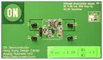
PCB layout is very important for switching converter
performance. All the converter’s external components
should be placed closed to the IC. The schematic, PCB
trace layout, and component placement of the step−up
DC−DC converter demonstration board are shown in
Figures 32 through 35 for PCB layout design reference.
The following guidelines should be observed:
1. Grounding
Single−point grounding should be used for the output
power return ground, the input power return ground, and
the device switch ground to reduce noise. The input ground
and output ground traces must be thick and short enough for
current to flow through. A ground plane should be used to
reduce ground bounce.
2. Power Traces
Low resistance conducting paths (short and thick traces)
should be used for the power carrying traces to reduce
power loss so as to improve efficiency (short and thick
traces for connecting the inductor L can also reduce stray
inductance). The path between C1, L1, D1, and C2 should
be kept short. The trace from L to LX pin of the IC should
also be kept short.
3. External Feedback Components
Feedback resistors R1 and R2, and feedforward capacitor
C3 should be located as close to the FB pin as possible to
minimize noise picked up by the FB pin. The ground
connection of the feedback resistor divider should be
connected directly to the GND pin.
4. Input Capacitor
The input capacitor should be located close to both the
input to the inductor and the VDD pin of the IC.
5. Output Capacitor
The output capacitor should be placed close to the output
terminals to obtain better smoothing effect on output ripple
voltage.
(eq. 14)
ESR
(eq. 16)
1
FSW(load)
20
PCB Layout Guidelines
D1
LX
5
NCP1406
VRIPPLE + IPK
CFF [
MBR0530LT1
TP3
VOUT
25 V
C2
3.3 mF
GND
4
R2
TP4
GND
Figure 32. Step−Up Converter Demonstration Board Schematic
http://onsemi.com
14
�NCP1406, NCV1406
Figure 33. Step−Up Converter Demonstration Board
Top Layer Component Silkscreen
Figure 34. Step−Up Converter Demonstration Board
Top Layer Copper
Figure 35. Step−Up Converter Demonstration Board
Bottom Layer Copper
http://onsemi.com
15
�NCP1406, NCV1406
Components and Suppliers
Output
Voltage
Parts
15 V
C1
Supplier
Panasonic
TDK
C2
Panasonic
TDK
C3
Panasonic
TDK
D1
ON Semiconductor
L1
Sumida Electric Co.
TDK
25 V
Part Number
Description
Website
ECJ2FB0J106M
Ceramic Capacitor 0805, 10 mF/6.3 V
www.panasonic.com
C1608X5R0J475MT
Ceramic Capacitor 0603, 10 mF/6.3 V
www.component.tdk.com
ECJ3YB1E475M
Ceramic Capacitor 1206, 4.7 mF/25 V
www.panasonic.com
C3216X5R1E475MT
Ceramic Capacitor 1206, 4.7 mF/25 V
www.component.tdk.com
ECJ1VC1H560K
Ceramic Capacitor 0603, 56 pF/50 V
www.panasonic.com
C1005C0G1H560JT
Ceramic Capacitor 0402, 56 pF/50 V
www.component.tdk.com
MBR0520LT1
Schottky Power Rectifier 20 V/500 mA
www.onsemi.com
CMD4D11−100MC
Inductor 10 mH 1.2 mm Low Profile
www.sumida.com
VLF4012AT−100MR79
Inductor 10 mH 1.2 mm Low Profile
www.component.tdk.com
R1
Panasonic
ERJ3GEYJ135V
Resistor 0603, 1.3 MW
www.panasonic.com
R2
Panasonic
ERJ3GEYJ114V
Resistor 0603, 110 kW
www.panasonic.com
U1
ON Semiconductor
NCP1406SNT1
25 V Step−up DC−DC Converter
C1
Panasonic
ECJ2FB0J106M
Ceramic Capacitor 0805, 10 mF/6.3 V
www.panasonic.com
C1608X5R0J475MT
Ceramic Capacitor 0603, 10 mF/6.3 V
www.component.tdk.com
ECJ5YB1H335M
Ceramic Capacitor 1812, 3.3 mF/50 V
www.panasonic.com
C3225X5R1H475MT
Ceramic Capacitor 1206, 3.3 mF/50 V
www.component.tdk.com
ECJ1VC1H151K
Ceramic Capacitor 0603, 150 pF/50 V
www.panasonic.com
C1005C0G1H151JT
Ceramic Capacitor 0402, 150 pF/50 V
www.component.tdk.com
MBR0530LT1
Schottky Power Rectifier 30 V/500 mA
www.onsemi.com
TDK
C2
Panasonic
TDK
C3
Panasonic
TDK
D1
ON Semiconductor
L1
Sumida Electric Co.
TDK
www.onsemi.com
CMD4D11−100MC
Inductor 10 mH 1.2 mm Low Profile
www.sumida.com
VLF4012AT−100MR79
Inductor 10 mH 1.2 mm Low Profile
www.component.tdk.com
R1
Panasonic
ERJ3GEYJ225V
Resistor 0603, 2.2 MW
www.panasonic.com
R2
Panasonic
ERJ3GEYJ114V
Resistor 0603, 110 kW
www.panasonic.com
U1
ON Semiconductor
NCP1406SNT1G
25 V Step−up DC−DC Converter
http://onsemi.com
16
www.onsemi.com
�NCP1406, NCV1406
OTHER APPLICATION CIRCUITS
L 8.2 mH
C1
2.2 mF
VIN
2.0 V to 5.5 V
D3
FB
2
VDD
3
D1
LX
5
NCP1406
CE
1
CIN
10 mF
D2
VOUT
−15 V
COUT
4.7 mF
25 V
6.0 mA at VIN = 2.0 V
40 mA at VIN = 5.5 V
C3
C2
2.2 mF
1000 pF
GND
4
R1
ǒ
Ǔ
R1
VOUT [ * 1.19
)1 )1
R2
R2
L: CR43−8R2MC, Sumida
CIN: ECJ2FB0J106M, Panasonic
COUT: ECJ3YB1E475M, Panasonic
C1: ECJ2FB1C225K, Panasonic
C2: ECJ2FB1C225K, Panasonic
C3: ECJ1VC1H102J, Panasonic
D1, D2: MBR0520LT1, ON Semiconductor
D3: MBR0520LT1 x 2, ON Semiconductor
Figure 36. Positive−to−Negative Output Converter for Negative LCD Bias
D2
D3
C5
4.7 mF
25 V
C4
L1 10 mH
C1
10 mF
6.3 V
ON
5 pF to
1000 pF
CE
1
JP1
OFF
C3
R1
FB
2
R2 VDD
3
LX
5
U1
NCP1406
VIN
2.0 V to 5.5 V
2.2 mF
GND
4
D1
C2
4.7 mF
25 V
ǒ
VOUT2
−15 V
2.0 mA at VIN = 2.0 V
5.0 mA at VIN = 2.4 V
10 mA at VIN = 3.0 V
VOUT1
15 V
2.0 mA at VIN = 2.0 V
5.0 mA at VIN = 2.4 V
10 mA at VIN = 3.0 V
Ǔ
R1
VOUT1 + 1.19
)1
R2
VOUT2 [ −VOUT1 ) 0.3
L: CR43−100MC, Sumida
C1: ECJ2FB0J106M, Panasonic
C2, C5: ECJ3YB1E475M, Panasonic
C3: ECJ1VC1H102J, Panasonic
C4: ECJ2FB1C225K, Panasonic
D1: MBR0520LT1, ON Semiconductor
D2, D3: MBR0520LT1 x 2, ON Semiconductor
R1: 1.3 MW
R2: 110 kW
Figure 37. +15 V, −15 V Outputs Converter for LCD Bias Supply
http://onsemi.com
17
�NCP1406, NCV1406
D4
D5
VOUT2
−7.5 V
C7
10 mF 10 mA at VIN = 3.0 V
16 V
C5
L1 10 mH
C1
10 mF
6.3 V
ON
C4
2.2 mF
820 pF
CE
1
JP1
C3
OFF
R1
FB
2
R2 VDD
3
D3
C6
10 mF
16 V
D2
LX
5
U1
NCP1406
VIN
3.0 V to 5.5 V
2.2 mF
VOUT1
15 V
10 mA at VIN = 3.0 V
D1
C2
2.2 mF
16 V
GND
4
C9
L: CR43−100MC, Sumida
C1: ECJ2FB0J106M, Panasonic
C6, C7: ECJ3YB1C106M, Panasonic
C3: ECJ1VC1H821J, Panasonic
C2, C4, C5: ECJ2FB1C225K, Panasonic
D1, D2, D3, D4, D5: MBR0520LT1, ON Semiconductor
R1: 1.3 MW
R2: 110 kW
ǒ
Ǔ
R1
VOUT1 + 1.19
)1
R2
V
VOUT2 [ − OUT1
2
Figure 38. +15 V, −7.5 V Outputs Converter for CCD Supply Circuit
TP2
GND
L1 4.7 mH
C1
22 mF
6.3 V
Control
Signal
D1
JP1
ON
CE
CE
1
OFF
FB
2
VDD
3
R2
100 kW
TP3
VOUT
ILED
100 mA
LX
5
U1
NCP1406
TP1
VIN
3.0 V to 5.5 V
U1: NCP1406, ON Semiconductor
D1: MBR0520LT1, ON Semiconductor
L1: CR43−4R7MC, Sumida
C1: ECJHVB0J226M, Panasonic
C2: ECJ3YB1C106M, Panasonic
LED1, LED2, LED3: LWH1033 (Luxpia)
R1: 12 W
R2: 100 kW
C2
White LED x 3
GND
4
ILED(DC) +
1.19 V
R1
Figure 39. White LEDs Driver Circuit
http://onsemi.com
18
TP4
GND
10 mF
16 V
R1
12 W
�MECHANICAL CASE OUTLINE
PACKAGE DIMENSIONS
TSOP−5
CASE 483
ISSUE N
5
1
SCALE 2:1
NOTES:
1. DIMENSIONING AND TOLERANCING PER ASME
Y14.5M, 1994.
2. CONTROLLING DIMENSION: MILLIMETERS.
3. MAXIMUM LEAD THICKNESS INCLUDES LEAD FINISH
THICKNESS. MINIMUM LEAD THICKNESS IS THE
MINIMUM THICKNESS OF BASE MATERIAL.
4. DIMENSIONS A AND B DO NOT INCLUDE MOLD
FLASH, PROTRUSIONS, OR GATE BURRS. MOLD
FLASH, PROTRUSIONS, OR GATE BURRS SHALL NOT
EXCEED 0.15 PER SIDE. DIMENSION A.
5. OPTIONAL CONSTRUCTION: AN ADDITIONAL
TRIMMED LEAD IS ALLOWED IN THIS LOCATION.
TRIMMED LEAD NOT TO EXTEND MORE THAN 0.2
FROM BODY.
D 5X
NOTE 5
2X
DATE 12 AUG 2020
0.20 C A B
0.10 T
M
2X
0.20 T
5
B
1
4
2
B
S
3
K
DETAIL Z
G
A
A
TOP VIEW
DIM
A
B
C
D
G
H
J
K
M
S
DETAIL Z
J
C
0.05
H
C
SIDE VIEW
SEATING
PLANE
END VIEW
GENERIC
MARKING DIAGRAM*
SOLDERING FOOTPRINT*
0.95
0.037
MILLIMETERS
MIN
MAX
2.85
3.15
1.35
1.65
0.90
1.10
0.25
0.50
0.95 BSC
0.01
0.10
0.10
0.26
0.20
0.60
0_
10 _
2.50
3.00
1.9
0.074
5
5
XXXAYWG
G
1
1
Analog
2.4
0.094
XXX = Specific Device Code
A
= Assembly Location
Y
= Year
W = Work Week
G
= Pb−Free Package
1.0
0.039
XXX MG
G
Discrete/Logic
XXX = Specific Device Code
M = Date Code
G
= Pb−Free Package
(Note: Microdot may be in either location)
0.7
0.028
SCALE 10:1
mm Ǔ
ǒinches
*For additional information on our Pb−Free strategy and soldering
details, please download the ON Semiconductor Soldering and
Mounting Techniques Reference Manual, SOLDERRM/D.
DOCUMENT NUMBER:
DESCRIPTION:
98ARB18753C
TSOP−5
*This information is generic. Please refer to
device data sheet for actual part marking.
Pb−Free indicator, “G” or microdot “ G”,
may or may not be present.
Electronic versions are uncontrolled except when accessed directly from the Document Repository.
Printed versions are uncontrolled except when stamped “CONTROLLED COPY” in red.
PAGE 1 OF 1
ON Semiconductor and
are trademarks of Semiconductor Components Industries, LLC dba ON Semiconductor or its subsidiaries in the United States and/or other countries.
ON Semiconductor reserves the right to make changes without further notice to any products herein. ON Semiconductor makes no warranty, representation or guarantee regarding
the suitability of its products for any particular purpose, nor does ON Semiconductor assume any liability arising out of the application or use of any product or circuit, and specifically
disclaims any and all liability, including without limitation special, consequential or incidental damages. ON Semiconductor does not convey any license under its patent rights nor the
rights of others.
© Semiconductor Components Industries, LLC, 2018
www.onsemi.com
�onsemi,
, and other names, marks, and brands are registered and/or common law trademarks of Semiconductor Components Industries, LLC dba “onsemi” or its affiliates
and/or subsidiaries in the United States and/or other countries. onsemi owns the rights to a number of patents, trademarks, copyrights, trade secrets, and other intellectual property.
A listing of onsemi’s product/patent coverage may be accessed at www.onsemi.com/site/pdf/Patent−Marking.pdf. onsemi reserves the right to make changes at any time to any
products or information herein, without notice. The information herein is provided “as−is” and onsemi makes no warranty, representation or guarantee regarding the accuracy of the
information, product features, availability, functionality, or suitability of its products for any particular purpose, nor does onsemi assume any liability arising out of the application or use
of any product or circuit, and specifically disclaims any and all liability, including without limitation special, consequential or incidental damages. Buyer is responsible for its products
and applications using onsemi products, including compliance with all laws, regulations and safety requirements or standards, regardless of any support or applications information
provided by onsemi. “Typical” parameters which may be provided in onsemi data sheets and/or specifications can and do vary in different applications and actual performance may
vary over time. All operating parameters, including “Typicals” must be validated for each customer application by customer’s technical experts. onsemi does not convey any license
under any of its intellectual property rights nor the rights of others. onsemi products are not designed, intended, or authorized for use as a critical component in life support systems
or any FDA Class 3 medical devices or medical devices with a same or similar classification in a foreign jurisdiction or any devices intended for implantation in the human body. Should
Buyer purchase or use onsemi products for any such unintended or unauthorized application, Buyer shall indemnify and hold onsemi and its officers, employees, subsidiaries, affiliates,
and distributors harmless against all claims, costs, damages, and expenses, and reasonable attorney fees arising out of, directly or indirectly, any claim of personal injury or death
associated with such unintended or unauthorized use, even if such claim alleges that onsemi was negligent regarding the design or manufacture of the part. onsemi is an Equal
Opportunity/Affirmative Action Employer. This literature is subject to all applicable copyright laws and is not for resale in any manner.
PUBLICATION ORDERING INFORMATION
LITERATURE FULFILLMENT:
Email Requests to: orderlit@onsemi.com
onsemi Website: www.onsemi.com
◊
TECHNICAL SUPPORT
North American Technical Support:
Voice Mail: 1 800−282−9855 Toll Free USA/Canada
Phone: 011 421 33 790 2910
Europe, Middle East and Africa Technical Support:
Phone: 00421 33 790 2910
For additional information, please contact your local Sales Representative
�


 工商网监
湘ICP备2023018690号
工商网监
湘ICP备2023018690号
