NCP1588, NCP1589
Low Voltage Synchronous
Buck Controller
The NCP158x is a low cost PWM controller designed to operate
from a 5 V or 12 V supply. This device is capable of producing an
output voltage as low as 0.8 V. This device is capable of converting
voltage from as low as 2.5 V. This 10-pin device provides an optimal
level of integration to reduce size and cost of the power supply.
Features include a 1.5 A gate driver design and an internally set
300�kHz oscillator. In addition to the 1.5 A gate drive capability, other
efficiency enhancing features of the gate driver include adaptive
non-overlap circuitry. The NCP158x also incorporates an externally
compensated error amplifier. Protection features include
programmable short circuit protection and undervoltage lockout
(UVLO).
Features
•�VCC Range from 4.5 to 13.2 V
•�300 kHz Internal Oscillator
•�Boost Pin Operates to 26.4 V
•�Voltage Mode PWM Control
•�Precision 0.8 V Internal Reference
•�Adjustable Output Voltage
•�Internal 1.5 A Gate Drivers
•�80% Max Duty Cycle
•�Input Under Voltage Lockout
•�Programmable Current Limit
•�This is a Pb-Free Device
http://onsemi.com
MARKING DIAGRAMS
158x
ALYWG
G
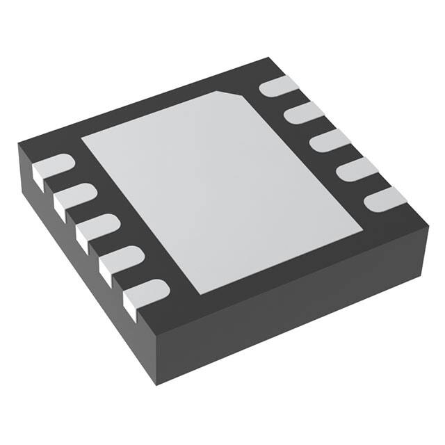
DFN10
CASE 485C
158x
x
A
L
Y
W
G
= Specific Device Code
= 8 or 9
= Assembly Location
= Wafer Lot
= Year
= Work Week
= Pb-Free Device
(Note: Microdot may be in either location)
PIN CONNECTIONS
Applications
•�Graphics Cards
•�Desktop Computers
•�Servers / Networking
•�DSP & FPGA Power Supply
•�DC-DC Regulator Modules
PGOOD
BOOT
1
10
LX
2
9
VOS
UG
3
8
FB
LG
4
7
COMP/EN
GND
5
6
VCC
(Top View)
ORDERING INFORMATION
Device
Package
Shipping†
NCP1588MTR2G
DFN10
3000/Tape & Reel
(Pb-Free)
NCP1589MNTZG
DFN10
3000/Tape & Reel
(Pb-Free)
†For information on tape and reel specifications,
including part orientation and tape sizes, please
refer to our Tape and Reel Packaging Specifications
Brochure, BRD8011/D.
©� Semiconductor Components Industries, LLC, 2008
January, 2008 - Rev. 4
1
Publication Order Number:
NCP1588/D
�NCP1588, NCP1589
VIN = 2.5 V - 13.2 V
3x22mF
VBST = 4.5 V - 15 V
1500mF
VCC = 4.5 V - 13.2 V
1mF
2x0.22mF
1500mF
VCC
NTD4809
BOOT
PGOOD
0.1mF
COMP/EN
UG
R2
17.08kW
LG
GND
C3
0.014mF
R3
74.2W
R9
R10
2x1800mF
4.7nF
1.02k
R1
4.12kW
1.02k
R4
3.878kW
VOS
VOUT
1.65 V
1mH
2.2
FB
NTD4806
LX
C2
0.007mF
ROCSET
C1
0.0015mF
GND
Figure 1. Typical Application Diagram
PGOOD
PGOOD
MONITOR
OV and UV
VOS 9
±10% of Vref
±25% of Vref
0.8 V
(Vref)
POR
UVLO
8
-
+
+
0.8 V
(Vref)
+
LATCH
FAULT
FB
10
6
VCC
1
BOOT
3
UG
2
LX
4
LG
5
GND
VOCP
FAULT
R
S
PWM
OUT
Q
+
-
CLOCK
RAMP
COMP/EN
7
2V
+
SOFT
START
-
OSC
OSC
FAULT
Figure 2. Detailed Block Diagram
http://onsemi.com
2
VCC
�NCP1588, NCP1589
PIN FUNCTION DESCRIPTION
Pin No.
Symbol
Description
1
BOOT
Supply rail for the floating top gate driver. To form a boost circuit, use an external diode to bring the desired
input voltage to this pin (cathode connected to BOOT pin). Connect a capacitor (CBOOT) between this pin and
the LX pin. Typical values for CBOOT range from 0.1 mF to 1 mF. Ensure that CBOOT is placed near the IC.
2
LX
Switch node pin. This is the reference for the floating top gate driver. Connect this pin to the source of the top
MOSFET.
3
UG
Top gate MOSFET driver pin. Connect this pin to the gate of the top N-channel MOSFET.
4
LG
Bottom gate MOSFET driver pin. Connect this pin to the gate of the bottom N-channel MOSFET.
5
GND
IC ground reference. All control circuits are referenced to this pin.
6
VCC
Supply rail for the internal circuitry. Operating supply range is 4.5 V to 13.2 V. Decouple with a 1 mF capacitor
to GND. Ensure that this decoupling capacitor is placed near the IC.
7
COMP/EN
Compensation Pin. This is the output of the error amplifier (EA) and the non-inverting input of the PWM com‐
parator. Use this pin in conjunction with the FB pin to compensate the voltage-control feedback loop. Pull this
pin low for disable.
8
FB
9
VOS
10
PGOOD
This pin is the inverting input to the error amplifier. Use this pin in conjunction with the COMP pin to com‐
pensate the voltage-control feedback loop. Connect this pin to the output resistor divider (if used) or directly
to Vout.
Offset voltage pin from Vout.
Power Good output. Open drain type output that is flagged low if ±10% of Vout.
ABSOLUTE MAXIMUM RATINGS
Pin Name
Main Supply Voltage Input
Bootstrap Supply Voltage Input
Switching Node (Bootstrap Supply Return)
Symbol
VMAX
VMIN
VCC
15 V
-0.3 V
BOOT
30 V wrt/GND
38-40 V < 100 ns
15 V wrt/LX
-0.3 V
LX
25 V
30 V for < 100 ns
-5 V
High-Side Driver Output (Top Gate)
UG
30 V wrt/GND
15 V wrt/LX
40 V for < 100 ns
-0.3 V wrt/LX
Low-Side Driver Output (Bottom Gate)
LG
VCC + 0.3 V
-0.3 V
-2 V < 100 ns
FB, VOS
3.6 V
-0.3 V
COMP/EN
3.6 V
-0.3 V
PGOOD
7V
-0.3 V
Symbol
Value
Unit
Thermal Resistance, Junction-to-Ambient
RqJA
165
°C/W
Thermal Resistance, Junction-to-Case
Feedback, VOS
COMP/EN
PGOOD
MAXIMUM RATINGS
Rating
RqJC
45
°C/W
NCP1588 Operating Junction Temperature Range
TJ
0 to 150
°C
NCP1588 Operating Ambient Temperature Range
TA
-40 to 85
°C
Storage Temperature Range
Tstg
-55 to +150
°C
Moisture Sensitivity Level
MSL
3
-
Stresses exceeding Maximum Ratings may damage the device. Maximum Ratings are stress ratings only. Functional operation above the
Recommended Operating Conditions is not implied. Extended exposure to stresses above the Recommended Operating Conditions may affect
device reliability.
http://onsemi.com
3
�NCP1588, NCP1589
ELECTRICAL CHARACTERISTICS (-40°C < TA < 85°C, 0°C < TJ < 125°C; 4.5 V < VCC < 13.2 V, 4.5 V < BOOT < 26.4 V,
CUG = CLG = 1.0 nF (REF:NTD30N02), for min/max values unless otherwise noted.)
Characteristic
Conditions
Input Voltage Range
Boost Voltage Range
13.2 V wrt LX
Min
Typ
Max
Unit
4.5
13.2
V
4.5
26.4
V
4.0
mA
Supply Current
Quiescent Supply Current
VFB = 1.0 V, No Switching, VCC = 13.2 V
1.0
Boost Quiescent Current
VFB = 1.0 V, No Switching
140
mA
Undervoltage Lockout
UVLO Threshold
NCP1588
NCP1589
UVLO Hysteresis
NCP1588
NCP1589
VCC Rising Edge
3.8
3.9
4.0
4.1
0.37
0.2
V
V
Switching Regulator
VFB Feedback Voltage
NCP1588
NCP1589
(FB Tied to Comp. Measure FB Pin.)
Oscillator Frequency
0.792
0.7936
0.8
0.8
0.808
0.8064
V
270
300
330
kHz
Ramp-Amplitude Voltage
Minimum Duty Cycle
Maximum Duty Cycle
70
LG Minimum on Time
1.1
V
0
%
75
80
%
500
ns
80
dB
Error Amplifier
Open Loop DC Gain (Note 1)
70
Output Source Current
Output Sink Current
Vfb < 0.8 V
Vfb > 0.8 V
Input Offset Voltage (Note 1)
2.0
2.0
-2.0
Input Bias Current
Unity Gain Bandwidth (Note 1)
Disable Threshold
mA
0
2.0
mV
0.1
1.0
mA
15
NCP1588
NCP1589
0.3
0.6
Mhz
0.5
V
100
mA
0.8
Output Source Current During Disable
Gate Drivers
Upper Gate Source
VCC = 5 V, VUG - VLX = 2.5 V
1.5
Upper Gate Sink
W
1.4
Lower Gate Source
Lower Gate Sink
A
1.5
A
W
VCC = 12 V
1.0
UG Falling to LG Rising Delay
VCC = 12 V, UG-LX < 2.0 V, LG > 2.0 V
30
90
ns
LG Falling to UG Rising Delay
VCC = 12 V, LG < 2.0 V, UG > 2.0 V
30
60
ns
http://onsemi.com
4
�NCP1588, NCP1589
ELECTRICAL CHARACTERISTICS (-40°C < TA < 85°C, 0°C < TJ < 125°C; 4.5 V < VCC < 13.2 V, 4.5 V < BOOT < 26.4 V,
CUG = CLG = 1.0 nF (REF:NTD30N02), for min/max values unless otherwise noted.)
Characteristic
Conditions
Min
Typ
Max
Unit
7.0
ms
0.4
V
Soft-Start
Soft-Start time
3.0
Power Good
Output Saturation Voltage
IPG = 4 mA, VCC = 12 Vdc
OVP Threshold to Part Disable
1.0
V
UVP Threshold to Part Disable
0.6
V
OVP Threshold to PGOOD Output Low
0.88
V
UVP Threshold to PGOOD Output Low
0.72
V
10
mA
Overcurrent Protection
OC Current Source
Sourced from LG pin, before SS
1. Guaranteed by design but not tested in production.
http://onsemi.com
5
�NCP1588, NCP1589
TYPICAL CHARACTERISTICS
305
808
806
Vref REFERENCE (mV)
fSW, FREQUENCY (kHz)
VCC = 12 V
303
VCC = 5.0 V
301
299
297
804
802
800
Series 1
798
796
794
295
0
20
40
60
792
-40
80
TJ, JUNCTION TEMPERATURE (°C)
Figure 3. Oscillator Frequency (fSW) vs. Temperature
-556
-558
OCP THRESHOLD (mV)
3.5
3.0
ICC (mA)
85
Figure 4. Reference Voltage (Vref) vs.
Temperature
4.0
2.5
2.0
1.5
1.0
0
25
TJ, JUNCTION TEMPERATURE (°C)
-560
-562
-564
-566
-568
20
40
60
-570
0
80
20
40
60
TJ, JUNCTION TEMPERATURE (°C)
TJ, JUNCTION TEMPERATURE (°C)
Figure 5. ICC vs. Temperature
Figure 6. OCP Threshold with 55k Rset vs.
Temperature
http://onsemi.com
6
80
�NCP1588, NCP1589
APPLICATIONS INFORMATION
Overcurrent Protection (OCP)
Internal Soft –Start
The low-side RDSon sense is implemented by comparing
the voltage at the LX, at the end of LG on time to an
internally generated fixed voltage. If the phase voltage is
lower than OCP trip voltage, an overcurrent condition
occurs and a counter is initiated.
When the counter completes after two clock cycles, the
PWM logic and both HS-FET and LS-FET are turned off.
Power has to be recycled to exit out of the overcurrent fault.
The minimum turn-on time of the LS-FET is set to be
500 ns.
NCP158x allows to easily program an Overcurrent
Threshold ranging from 50 mV to 550 mV, simply by
adding a resistor (ROCSET) between LG and GND. During
a short period of time following VCC rising over UVLO
threshold, an internal 10 mA current (IOCSET, trimmed to
$5%) is sourced from LG pin, determining a voltage drop
across ROCSET. This voltage drop will be sampled and
internally held by the device as OverCurrent Threshold. The
OC setting procedure overall time length is about 4.2 ms.
Connecting a ROCSET resistor between LG and GND, the
programmed threshold will be:
The NCP158x features an internal soft-start function,
which reduces the inrush current and overshoot of the output
voltage. Figure 7. shows a typical soft-start sequence.
Soft-Start is achieved by ramping the internal reference
using the oscillator clock (64 steps from 0 V to 0.8 V of
Vref). The order of startup sequence is as follows: UVLO →
OCP programming → Comp voltage reach the lower end of
the Ramp voltage (1.45 V). The typical soft-start time is
4.2 ms. The internal soft-start is held low when the part is
in UVLO or Disable mode.
I OCth +
Power Good
Power Good is an open drain and active high output. This
output can be pulled up high to the appropriate level with an
external resistor. It monitors the output voltage through the
VOS pin. The PGOOD is flagged low for ±10% of Vout for
OV/UV trip points respectively. The separate VOS input is
not slowed down by the compensation on the VFB pin. The
PGOOD output can deliver a max of 4 mA sink current at
0.4 V when de-asserted. The PGOOD pin is held low during
soft-start. Once soft-start is complete PGOOD goes high if
there are no faults without any delays associated to it.
I OCSET @ R OCSET
Undervoltage Protection
R DS(on)
If the voltage at VOS pin drops below UV threshold, the
device turns off both HS and LS MOSFETs, latching the
condition. This requires a POR to recover.
RSET values range from 5 kW to 55 kW. In case ROCSET
is not connected, the device switches the OCP threshold to
a fixed 640 mV value: an internal safety clamp on BG is
triggered as soon as LG voltage reaches 700 mV, enabling
the 640 mV fixed threshold and ending OC setting phase.
The current trip threshold tolerance is ±25 mV. The accuracy
of the set point is best at the highest set point. The accuracy
will decrease as the set point decreases.
Overvoltage Protection
If the voltage at VOS pin rises over OV threshold (1V typ),
overvoltage protection turns off UG MOSFET and turns on
LG MOSFET. The LG MOSFET will be turned off as soon
as VOS goes below Vref/2 (0.4 V). The condition is latched,
and requires POR to recover. The device still controls the LG
MOSFET and can switch it on whenever VOS rises above
1.0 V.
http://onsemi.com
7
�NCP1588, NCP1589
4.3 V
3.7 V
VCC
UVLO
Fault
1.45 V
COMP
-0.7 V
700 mV
50 mV
OCP
UG
Program‐
mable
LG
VOUT
0.8 V
Vfb
UV
Monitor
POR
UVLO
SS
NORMAL
Figure 7. Typical Startup Sequence
http://onsemi.com
8
�NCP1588, NCP1589
VOS
1.0V
0.88V
0.8V
0.88V
0.8V
0.72V
0.6V
0.4V
PG
UG
LG
Overvoltage
Undervoltage
Figure 8. Typical Power Good Function
Feedback and Compensation
Design Example
The NCP158x allows the output voltage to be adjusted
from 0.8 V to 5.0 V via an external resistor divider network.
The controller will try to maintain 0.8 V at feedback pin.
Thus, if a resistor divider circuit was placed across the
feedback pin to VOUT, the controller will regulate the output
voltage proportional to the resistor divider network in order
to maintain 0.8 V at the FB pin. The same formula applies
to the VOS pin and the controller will maintain 0.8 V at the
VOS pin.
Voltage Mode Control Loop with TYPE III
Compensation
Converter Parameters:
Input Voltage: VIN = 5 V
Output Voltage: VOUT = 1.65 V
Switching Frequency: 300 kHz
Total Output Capacitance: COUT = 3600 mF
Total ESR: ESR = 6 mW
Output Inductance: LOUT: 1 mH
Ramp Amplitude: VRAMP = 1.1 V
VOUT
C1
R1
FB
R3
C3
R2
C2
R4
VOUT
Figure 9.
VCOMP
Vref
ǒVOUTVREF
Ǔ
* VREF
Figure 10.
a.. Set a target for the close loop bandwidth at 1/6th of
the switching frequency.
The same formula can be applied to the feedback resistors
at VOS.
R9 + R10
E/A
+
R4
The relationship between the resistor divider network
above and the output voltage is shown in the following
equation:
R4 + R1
R1
ǒVOUTVREF
Ǔ
* VREF
F cross_over :+ 50�kHz
http://onsemi.com
9
�NCP1588, NCP1589
Step 5: Place 2nd zero at the output filter double pole
frequency.
b.. Output Filter Double Pole Frequency
F lc :+
1
2 @ p @ Ǹ�L OUT @ C OUT�
R3 :+
Step 6: Place 2nd pole at half the switching frequency.
1
2 @ p @ C OUT @ C ESR
C3 :+
F ESR + 7.368�kHz
Step 2: Pick compensation DC gain (R2/R1) for desired
close loop bandwidth.
R4 :+
V RAMP :+ 1.1�V
Ǔǒ
V RAMP
@
F cross_over
F lc
Ǔ
R1 = 4.12 kW
R2 = 17.085 kW
R3 = 74.169 W
R4 = 3.878 kW
C1 = 0.0015 mF
C2 = 0.007 mF
C3 = 0.014 mF
NOTE: Recommend to change values to industry
standard component values.
2 @ ǸL OUT @ C OUT
R2
10 -3�mF
Step 4: Place 1st pole at ESR zero frequency.
C1 :+
C2
C2 @ R2 @ 2 @ p @ F ESR * 1
C1 + 1.542
V OUT * V REF
The Component values for Type III Compensation are:
Step 3: Place 1st zero at half the output filter double pole
frequency.
C2 + 7.024
V REF @ R1
R4 + 3.878�kW
R2 + 17.085�kW
C2 :+
ǒ�p @ R3 @ FSWǓ
Step 7: R4 is sized to maintain the feedback voltage to
Vref = 0.8 V.
R1 :+ 4.12�kW
V IN
1
C3 + 0.014�mF
Step 1: Set a value for R1 between 2 kW and 5 kW
ǒ
*1
lc
R3 + 74.169�W
c.. ESR Zero Frequency:
R2 :+ R1 @
SW
2@F
F lc + 2.653�kHz
F ESR :+
R1
F
10 -3�mF
http://onsemi.com
10
�MECHANICAL CASE OUTLINE
PACKAGE DIMENSIONS
DFN10, 3x3, 0.5P
CASE 485C
ISSUE F
SCALE 2:1
DATE 16 DEC 2021
GENERIC
MARKING DIAGRAM*
XXXXX
XXXXX
ALYWG
G
XXXXX = Specific Device Code
A
= Assembly Location
L
= Wafer Lot
*This information is generic. Please refer to
Y
= Year
device data sheet for actual part marking.
W
= Work Week
Pb−Free indicator, “G” or microdot “G”, may
G
= Pb−Free Package
or may not be present. Some products may
(Note: Microdot may be in either location) not follow the Generic Marking.
DOCUMENT NUMBER:
DESCRIPTION:
98AON03161D
Electronic versions are uncontrolled except when accessed directly from the Document Repository.
Printed versions are uncontrolled except when stamped “CONTROLLED COPY” in red.
DFN10, 3X3 MM, 0.5 MM PITCH
PAGE 1 OF 1
onsemi and
are trademarks of Semiconductor Components Industries, LLC dba onsemi or its subsidiaries in the United States and/or other countries. onsemi reserves
the right to make changes without further notice to any products herein. onsemi makes no warranty, representation or guarantee regarding the suitability of its products for any particular
purpose, nor does onsemi assume any liability arising out of the application or use of any product or circuit, and specifically disclaims any and all liability, including without limitation
special, consequential or incidental damages. onsemi does not convey any license under its patent rights nor the rights of others.
© Semiconductor Components Industries, LLC, 2019
www.onsemi.com
�onsemi,
, and other names, marks, and brands are registered and/or common law trademarks of Semiconductor Components Industries, LLC dba “onsemi” or its affiliates
and/or subsidiaries in the United States and/or other countries. onsemi owns the rights to a number of patents, trademarks, copyrights, trade secrets, and other intellectual property.
A listing of onsemi’s product/patent coverage may be accessed at www.onsemi.com/site/pdf/Patent−Marking.pdf. onsemi reserves the right to make changes at any time to any
products or information herein, without notice. The information herein is provided “as−is” and onsemi makes no warranty, representation or guarantee regarding the accuracy of the
information, product features, availability, functionality, or suitability of its products for any particular purpose, nor does onsemi assume any liability arising out of the application or use
of any product or circuit, and specifically disclaims any and all liability, including without limitation special, consequential or incidental damages. Buyer is responsible for its products
and applications using onsemi products, including compliance with all laws, regulations and safety requirements or standards, regardless of any support or applications information
provided by onsemi. “Typical” parameters which may be provided in onsemi data sheets and/or specifications can and do vary in different applications and actual performance may
vary over time. All operating parameters, including “Typicals” must be validated for each customer application by customer’s technical experts. onsemi does not convey any license
under any of its intellectual property rights nor the rights of others. onsemi products are not designed, intended, or authorized for use as a critical component in life support systems
or any FDA Class 3 medical devices or medical devices with a same or similar classification in a foreign jurisdiction or any devices intended for implantation in the human body. Should
Buyer purchase or use onsemi products for any such unintended or unauthorized application, Buyer shall indemnify and hold onsemi and its officers, employees, subsidiaries, affiliates,
and distributors harmless against all claims, costs, damages, and expenses, and reasonable attorney fees arising out of, directly or indirectly, any claim of personal injury or death
associated with such unintended or unauthorized use, even if such claim alleges that onsemi was negligent regarding the design or manufacture of the part. onsemi is an Equal
Opportunity/Affirmative Action Employer. This literature is subject to all applicable copyright laws and is not for resale in any manner.
PUBLICATION ORDERING INFORMATION
LITERATURE FULFILLMENT:
Email Requests to: orderlit@onsemi.com
onsemi Website: www.onsemi.com
◊
TECHNICAL SUPPORT
North American Technical Support:
Voice Mail: 1 800−282−9855 Toll Free USA/Canada
Phone: 011 421 33 790 2910
Europe, Middle East and Africa Technical Support:
Phone: 00421 33 790 2910
For additional information, please contact your local Sales Representative
�


 工商网监
湘ICP备2023018690号
工商网监
湘ICP备2023018690号
