NCP3418B
MOSFET Driver with Dual
Outputs for Synchronous
Buck Converters
The NCP3418B is a single Phase 12 V MOSFET gate driver
optimized to drive the gates of both high−side and low−side power
MOSFETs in a synchronous buck converter. The high−side and
low−side driver is capable of driving a 3000 pF load with a 25 ns
propagation delay and a 20 ns transition time.
With a wide operating voltage range, high or low side MOSFET
gate drive voltage can be optimized for the best efficiency. Internal
adaptive nonoverlap circuitry further reduces switching losses by
preventing simultaneous conduction of both MOSFETs.
The floating top driver design can accommodate VBST voltages as
high as 30 V, with transient voltages as high as 35 V. Both gate outputs
can be driven low by applying a low logic level to the Output Disable
(OD) pin. An Undervoltage Lockout function ensures that both driver
outputs are low when the supply voltage is low, and a Thermal
Shutdown function provides the IC with overtemperature protection.
The NCP3418B is pin−to−pin compatible with Analog Devices
ADP3418 with the following advantages:
http://onsemi.com
MARKING
DIAGRAMS
8
8
1
1
A
L
Y
W
G
• Faster Rise and Fall Times
• Thermal Shutdown for System Protection
• Internal Pulldown Resistor Suppresses Transient Turn On of Either
•
•
•
•
•
•
•
•
•
3418B
ALYW
G
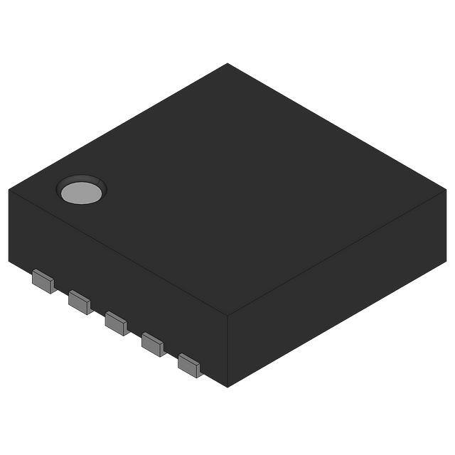
DFN−10
MN SUFFIX
CASE 485C
Features
MOSFET
Anti Cross−Conduction Protection Circuitry
Floating Top Driver Accommodates Boost Voltages of up to 30 V
One Input Signal Controls Both the Upper and Lower Gate Outputs
Output Disable Control Turns Off Both MOSFETs
Complies with VRM10.x and VRM11.x Specifications
Undervoltage Lockout
Thermal Shutdown
Thermally Enhanced Package Available
These are Pb−Free Devices
3418B
ALYW
G
SO−8
D SUFFIX
CASE 751
= Assembly Location
= Wafer Lot
= Year
= Work Week
= Pb−Free Package
PIN CONNECTIONS
1
BST
8
DRVH
IN
OD
SWN
PGND
VCC
DRVL
1
10
BST
IN
DRVH
SWN
OD
VCC
VCC
PGND
PGND
DRVL
(Top View)
ORDERING INFORMATION
Device
Package
Shipping†
NCP3418BDR2G
SO−8
(Pb−Free)
2500 Tape & Reel
NCP3418BMNR2G DFN−10
(Pb−Free)
3000 Tape & Reel
†For information on tape and reel specifications,
including part orientation and tape sizes, please
refer to our Tape and Reel Packaging Specification
Brochure, BRD8011/D.
© Semiconductor Components Industries, LLC, 2006
March, 2006 − Rev. 5
1
Publication Order Number:
NCP3418B/D
�NCP3418B
OD
3
VCC
TSD
1
BST
8
DRVH
7
SWN
4
VCC
5
DRVL
6
PGND
UVLO
IN
2
FALLING
EDGE
DELAY
FALLING
EDGE
DELAY
START
STOP
MONITOR
MONITOR
NON−OVERLAP
TIMERS
MIN DRVL
OFF TIMER
Figure 1. Block Diagram
PIN DESCRIPTION
SO−8
DFN−10
Symbol
Description
1
1
BST
Upper MOSFET Floating Bootstrap Supply. A capacitor connected between BST and SW pins holds
this bootstrap voltage for the high−side MOSFET as it is switched. The recommended capacitor value
is between 100 nF and 1.0 mF. An external diode is required with the NCP3418B.
2
2
IN
Logic−Level Input. This pin has primary control of the drive outputs.
3
3
OD
Output Disable. When low, normal operation is disabled forcing DRVH and DRVL low.
4
4
VCC
Input Supply. A 1.0 mF ceramic capacitor should be connected from this pin to PGND.
−
5
VCC
Input Supply. A 1.0 mF ceramic capacitor should be connected from this pin to PGND.
5
6
DRVL
Output drive for the lower MOSFET.
6
7
PGND
Power Ground. Should be closely connected to the source of the lower MOSFET.
−
8
PGND
Power Ground. Should be closely connected to the source of the lower MOSFET.
7
9
SWN
Switch Node. Connect to the source of the upper MOSFET.
8
10
DRVH
Output drive for the upper MOSFET.
http://onsemi.com
2
�NCP3418B
MAXIMUM RATINGS
Rating
Value
Unit
Operating Ambient Temperature, TA
0 to 85
°C
Operating Junction Temperature, TJ (Note 1)
0 to 150
°C
45
123
°C/W
°C/W
7.5
55
°C/W
°C/W
−65 to 150
°C
260 peak
°C
1
−
Package Thermal Resistance: SO−8
Junction−to−Case, RqJC
Junction−to−Ambient, RqJA (2−Layer Board)
Package Thermal Resistance: DFN−10 (Note 2)
Junction−to−Case, RqJC (From die to exposed pad)
Junction−to−Ambient, RqJA
Storage Temperature Range, TS
Lead Temperature Soldering (10 sec): Reflow (SMD styles only)
Pb−Free (Note 3)
JEDEC Moisture Sensitivity Level
SO−8 (260 peak profile)
Maximum ratings are those values beyond which device damage can occur. Maximum ratings applied to the device are individual stress limit
values (not normal operating conditions) and are not valid simultaneously. If these limits are exceeded, device functional operation is not implied,
damage may occur and reliability may be affected.
1. Internally limited by thermal shutdown, 150°C min.
2. 2 layer board, 1 in2 Cu, 1 oz thickness.
3. 60−180 seconds minimum above 237°C.
NOTE: This device is ESD sensitive. Use standard ESD precautions when handling.
MAXIMUM RATINGS
Pin Symbol
Pin Name
VMAX
VMIN
VCC
Main Supply Voltage Input
15 V
−0.3 V
BST
Bootstrap Supply Voltage Input
30 V wrt/PGND
35 V v 50 ns wrt/PGND
15 V wrt/SW
−0.3 V wrt/SW
SW
Switching Node
(Bootstrap Supply Return)
30 V
−1.0 V DC
−10 V< 200 ns
DRVH
High−Side Driver Output
BST + 0.3 V
35 V v 50 ns wrt/PGND
15 V wrt/SW
−0.3 V wrt/SW
DRVL
Low−Side Driver Output
VCC + 0.3 V
−0.3 V DC
−2.0 V < 200 ns
IN
DRVH and DRVL Control Input
VCC + 0.3 V
−0.3 V
OD
Output Disable
VCC + 0.3 V
−0.3 V
PGND
Ground
0V
0V
NOTE:
All voltages are with respect to PGND except where noted.
http://onsemi.com
3
�NCP3418B
ELECTRICAL CHARACTERISTICS (Note 4) (VCC = 12 V, TA = 0°C to +85°C, TJ = 0°C to +125°C unless otherwise noted.)
Characteristic
Symbol
Condition
Min
Typ
Max
Unit
Supply Voltage Range
VCC
−
4.6
−
13.2
V
Supply Current
ISYS
BST = 12 V, IN = 0 V
−
2.0
6.0
mA
Input Voltage High
−
−
2.0
−
−
V
Input Voltage Low
−
−
−
−
0.8
V
Hysteresis
−
−
−
500
−
mV
Input Current
−
No internal pull−up or pull−down resistors
−1.0
−
+1.0
mA
tpdlOD
tpdhOD
−
30
30
50
50
60
60
ns
ns
Input Voltage High
−
−
2.0
−
−
V
Input Voltage Low
−
−
−
−
0.8
V
Hysteresis
−
−
−
500
−
mV
Input Current
−
No internal pull−up or pull−down resistors
−1.0
−
+1.0
mA
Output Resistance, Sourcing Current
−
VBST − VSW = 12 V (Note 7)
−
1.8
3.0
W
Output Resistance, Sinking Current
−
VBST − VSW = 12 V (Note 7)
−
1.0
2.5
W
trDRVH
tfDRVH
VBST − VSW = 12 V, CLOAD = 3.0 nF
(See Figure 3)
−
−
16
11
25
15
ns
ns
tpdhDRVH
tpdlDRVH
VBST − VSW = 12 V
−
−
30
25
60
45
ns
ns
Output Resistance, Sourcing Current
−
VCC = 12 V (Note 7)
−
1.8
3.0
W
Output Resistance, Sinking Current
−
VCC − VSW = 12 V (Note 7)
−
1.0
2.5
W
Timeout Delay
−
DRVH−SW = 0
−
85
−
ns
trDRVL
tfDRVL
CLOAD = 3.0 nF
(See Figure 3)
−
−
16
11
25
15
ns
ns
tpdhDRVL
tpdlDRVL
(See Figure 3)
−
−
30
20
60
30
ns
ns
UVLO Startup
−
−
3.7
3.9
4.4
V
UVLO Shutdown
−
−
3.2
3.5
3.9
V
Hysteresis
−
−
0.3
0.4
0.7
V
−
(Note 7)
150
170
−
°C
(Note 7)
−
20
−
°C
Supply
OD Input
Propagation Delay Time (Note 5)
PWM Input
High−Side Driver
Transition Times (Note 5)
Propagation Delay (Notes 5 & 6)
Low−Side Driver
Transition Times
Propagation Delay
Undervoltage Lockout
Thermal Shutdown
Over Temperature Protection
Hysteresis
4.
5.
6.
7.
All limits at temperature extremes are guaranteed via correlation using standard Statistical Quality Control (SQC).
AC specifications are guaranteed by characterization, but not production tested.
For propagation delays, “tpdh’’ refers to the specified signal going high; “tpdl’’ refers to it going low.
GBD: Guaranteed by design; not tested in production.
Specifications subject to change without notice.
http://onsemi.com
4
�NCP3418B
OD
tpdlOD
tpdhOD
90%
DRVH
or
DRVL
10%
Figure 2. Output Disable Timing Diagram
IN
tpdlDRVL
DRVL
tfDRVL
90%
90%
2V
10%
10%
tpdhDRVH
trDRVH
tpdlDRVH
90%
trDRVL
tfDRVH
90%
DRVH−SW
2V
10%
10%
tpdhDRVL
SW
Figure 3. Nonoverlap Timing Diagram
APPLICATIONS INFORMATION
Theory of Operation
High−Side Driver
The NCP3418B is a single phase MOSFET driver designed
for driving two N−channel MOSFETs in a synchronous buck
converter topology. The NCP3418B will operate from 5 V or
12 V, but it has been optimized for high current multi−phase
buck regulators that convert 12 Volt rail directly to the core
voltage required by complex logic chips. A single PWM input
signal is all that is required to properly drive the high−side and
the low−side MOSFETs. Each driver is capable of driving a
3.3 nF load at frequencies up to 500 kHz.
The high−side driver is designed to drive a floating low
RDS(on) N−channel MOSFET. The gate voltage for the high
side driver is developed by a bootstrap circuit referenced to
Switch Node (SW) pin.
The bootstrap circuit is comprised of an external diode,
and an external bootstrap capacitor. When the NCP3418B is
starting up, the SW pin is at ground, so the bootstrap
capacitor will charge up to VCC through the bootstrap diode
See Figure 4. When the PWM input goes high, the high−side
driver will begin to turn on the high−side MOSFET using the
stored charge of the bootstrap capacitor. As the high−side
MOSFET turns on, the SW pin will rise. When the high−side
MOSFET is fully on, the switch node will be at 12 volts, and
the BST pin will be at 12 volts plus the charge of the
bootstrap capacitor (approaching 24 volts).
The bootstrap capacitor is recharged when the switch
node goes low during the next cycle.
Low−Side Driver
The low−side driver is designed to drive a
ground−referenced low RDS(on) N−Channel MOSFET. The
voltage rail for the low−side driver is internally connected to
the VCC supply and PGND.
http://onsemi.com
5
�NCP3418B
Safety Timer and Overlap Protection Circuit
Input Pins
It is very important that MOSFETs in a synchronous buck
regulator do not both conduct at the same time. Excessive
shoot−through or cross conduction can damage the
MOSFETs, and even a small amount of cross conduction
will cause a decrease in the power conversion efficiency.
The NCP3418B prevents cross conduction by monitoring
the status of the external mosfets and applying the
appropriate amount of “dead−time” or the time between the
turn off of one MOSFET and the turn on of the other
MOSFET.
When the PWM input pin goes high, DRVL will go low
after a propagation delay (tpdlDRVL). The time it takes for
the low−side MOSFET to turn off (tfDRVL) is dependent on
the total charge on the low−side MOSFET gate. The
NCP3418B monitors the gate voltage of both MOSFETs and
the switchnode voltage to determine the conduction status of
the MOSFETs. Once the low−side MOSFET is turned off an
internal timer will delay (tpdhDRVH) the turn on of the
high−side MOSFET
Likewise, when the PWM input pin goes low, DRVH will
go low after the propagation delay (tpdDRVH). The time to
turn off the high−side MOSFET (tfDRVH) is dependent on
the total gate charge of the high−side MOSFET. A timer will
be triggered once the high−side mosfet has stopped
conducting, to delay (tpdhDRVL) the turn on of the
low−side MOSFET
The PWM input and the Output Disable pins of the
NCP3418B have internal protection for Electro Static
Discharge (ESD), but in normal operation they present a
relatively high input impedance. If the PWM controller does
not have internal pull−down resistors, they should be added
externally to ensure that the driver outputs do not go high
before the controller has reached its under voltage lockout
threshold. The NCP5381 controller does include a passive
internal pull−down resistor on the drive−on output pin.
Bootstrap Circuit
The bootstrap circuit uses a charge storage capacitor
(CBST) and the internal (or an external) diode. Selection of
these components can be done after the high−side MOSFET
has been chosen. The bootstrap capacitor must have a
voltage rating that is able to withstand twice the maximum
supply voltage. A minimum 50 V rating is recommended.
The capacitance is determined using the following equation:
CBST +
QGATE
DVBST
where QGATE is the total gate charge of the high−side
MOSFET, and DVBST is the voltage droop allowed on the
high−side MOSFET drive. For example, a NTD60N03 has
a total gate charge of about 30 nC. For an allowed droop of
300 mV, the required bootstrap capacitance is 100 nF. A
good quality ceramic capacitor should be used.
The bootstrap diode must be rated to withstand the
maximum supply voltage plus any peak ringing voltages
that may be present on SW. The average forward current can
be estimated by:
Power Supply Decoupling
The NCP3418B can source and sink relatively large
currents to the gate pins of the external MOSFETs. In order
to maintain a constant and stable supply voltage (Vcc) a low
ESR capacitor should be placed near the power and ground
pins. A 1 mF to 4.7 mF multi layer ceramic capacitor (MLCC)
is usually sufficient.
IF(AVG) + QGATE
fMAX
where fMAX is the maximum switching frequency of the
controller. The peak surge current rating should be checked
in−circuit, since this is dependent on the source impedance
of the 12 V supply and the ESR of CBST.
12 V
12 V
NCP3418
4
Output Enable
PWM in
BST
DRVH
SW
OD
DRVL
2
IN PGND
3
Vcc
1
8
7
5
6
Vout
Figure 4. NCP3418 Example Circuit
http://onsemi.com
6
�MECHANICAL CASE OUTLINE
PACKAGE DIMENSIONS
DFN10, 3x3, 0.5P
CASE 485C
ISSUE F
SCALE 2:1
DATE 16 DEC 2021
GENERIC
MARKING DIAGRAM*
XXXXX
XXXXX
ALYWG
G
XXXXX = Specific Device Code
A
= Assembly Location
L
= Wafer Lot
*This information is generic. Please refer to
Y
= Year
device data sheet for actual part marking.
W
= Work Week
Pb−Free indicator, “G” or microdot “G”, may
G
= Pb−Free Package
or may not be present. Some products may
(Note: Microdot may be in either location) not follow the Generic Marking.
DOCUMENT NUMBER:
DESCRIPTION:
98AON03161D
Electronic versions are uncontrolled except when accessed directly from the Document Repository.
Printed versions are uncontrolled except when stamped “CONTROLLED COPY” in red.
DFN10, 3X3 MM, 0.5 MM PITCH
PAGE 1 OF 1
onsemi and
are trademarks of Semiconductor Components Industries, LLC dba onsemi or its subsidiaries in the United States and/or other countries. onsemi reserves
the right to make changes without further notice to any products herein. onsemi makes no warranty, representation or guarantee regarding the suitability of its products for any particular
purpose, nor does onsemi assume any liability arising out of the application or use of any product or circuit, and specifically disclaims any and all liability, including without limitation
special, consequential or incidental damages. onsemi does not convey any license under its patent rights nor the rights of others.
© Semiconductor Components Industries, LLC, 2019
www.onsemi.com
�MECHANICAL CASE OUTLINE
PACKAGE DIMENSIONS
SOIC−8 NB
CASE 751−07
ISSUE AK
8
1
SCALE 1:1
−X−
DATE 16 FEB 2011
NOTES:
1. DIMENSIONING AND TOLERANCING PER
ANSI Y14.5M, 1982.
2. CONTROLLING DIMENSION: MILLIMETER.
3. DIMENSION A AND B DO NOT INCLUDE
MOLD PROTRUSION.
4. MAXIMUM MOLD PROTRUSION 0.15 (0.006)
PER SIDE.
5. DIMENSION D DOES NOT INCLUDE DAMBAR
PROTRUSION. ALLOWABLE DAMBAR
PROTRUSION SHALL BE 0.127 (0.005) TOTAL
IN EXCESS OF THE D DIMENSION AT
MAXIMUM MATERIAL CONDITION.
6. 751−01 THRU 751−06 ARE OBSOLETE. NEW
STANDARD IS 751−07.
A
8
5
S
B
0.25 (0.010)
M
Y
M
1
4
−Y−
K
G
C
N
X 45 _
SEATING
PLANE
−Z−
0.10 (0.004)
H
M
D
0.25 (0.010)
M
Z Y
S
X
J
S
8
8
1
1
IC
4.0
0.155
XXXXX
A
L
Y
W
G
IC
(Pb−Free)
= Specific Device Code
= Assembly Location
= Wafer Lot
= Year
= Work Week
= Pb−Free Package
XXXXXX
AYWW
1
1
Discrete
XXXXXX
AYWW
G
Discrete
(Pb−Free)
XXXXXX = Specific Device Code
A
= Assembly Location
Y
= Year
WW
= Work Week
G
= Pb−Free Package
*This information is generic. Please refer to
device data sheet for actual part marking.
Pb−Free indicator, “G” or microdot “G”, may
or may not be present. Some products may
not follow the Generic Marking.
1.270
0.050
SCALE 6:1
INCHES
MIN
MAX
0.189
0.197
0.150
0.157
0.053
0.069
0.013
0.020
0.050 BSC
0.004
0.010
0.007
0.010
0.016
0.050
0 _
8 _
0.010
0.020
0.228
0.244
8
8
XXXXX
ALYWX
G
XXXXX
ALYWX
1.52
0.060
0.6
0.024
MILLIMETERS
MIN
MAX
4.80
5.00
3.80
4.00
1.35
1.75
0.33
0.51
1.27 BSC
0.10
0.25
0.19
0.25
0.40
1.27
0_
8_
0.25
0.50
5.80
6.20
GENERIC
MARKING DIAGRAM*
SOLDERING FOOTPRINT*
7.0
0.275
DIM
A
B
C
D
G
H
J
K
M
N
S
mm Ǔ
ǒinches
*For additional information on our Pb−Free strategy and soldering
details, please download the ON Semiconductor Soldering and
Mounting Techniques Reference Manual, SOLDERRM/D.
STYLES ON PAGE 2
DOCUMENT NUMBER:
DESCRIPTION:
98ASB42564B
SOIC−8 NB
Electronic versions are uncontrolled except when accessed directly from the Document Repository.
Printed versions are uncontrolled except when stamped “CONTROLLED COPY” in red.
PAGE 1 OF 2
onsemi and
are trademarks of Semiconductor Components Industries, LLC dba onsemi or its subsidiaries in the United States and/or other countries. onsemi reserves
the right to make changes without further notice to any products herein. onsemi makes no warranty, representation or guarantee regarding the suitability of its products for any particular
purpose, nor does onsemi assume any liability arising out of the application or use of any product or circuit, and specifically disclaims any and all liability, including without limitation
special, consequential or incidental damages. onsemi does not convey any license under its patent rights nor the rights of others.
© Semiconductor Components Industries, LLC, 2019
www.onsemi.com
�SOIC−8 NB
CASE 751−07
ISSUE AK
DATE 16 FEB 2011
STYLE 1:
PIN 1. EMITTER
2. COLLECTOR
3. COLLECTOR
4. EMITTER
5. EMITTER
6. BASE
7. BASE
8. EMITTER
STYLE 2:
PIN 1. COLLECTOR, DIE, #1
2. COLLECTOR, #1
3. COLLECTOR, #2
4. COLLECTOR, #2
5. BASE, #2
6. EMITTER, #2
7. BASE, #1
8. EMITTER, #1
STYLE 3:
PIN 1. DRAIN, DIE #1
2. DRAIN, #1
3. DRAIN, #2
4. DRAIN, #2
5. GATE, #2
6. SOURCE, #2
7. GATE, #1
8. SOURCE, #1
STYLE 4:
PIN 1. ANODE
2. ANODE
3. ANODE
4. ANODE
5. ANODE
6. ANODE
7. ANODE
8. COMMON CATHODE
STYLE 5:
PIN 1. DRAIN
2. DRAIN
3. DRAIN
4. DRAIN
5. GATE
6. GATE
7. SOURCE
8. SOURCE
STYLE 6:
PIN 1. SOURCE
2. DRAIN
3. DRAIN
4. SOURCE
5. SOURCE
6. GATE
7. GATE
8. SOURCE
STYLE 7:
PIN 1. INPUT
2. EXTERNAL BYPASS
3. THIRD STAGE SOURCE
4. GROUND
5. DRAIN
6. GATE 3
7. SECOND STAGE Vd
8. FIRST STAGE Vd
STYLE 8:
PIN 1. COLLECTOR, DIE #1
2. BASE, #1
3. BASE, #2
4. COLLECTOR, #2
5. COLLECTOR, #2
6. EMITTER, #2
7. EMITTER, #1
8. COLLECTOR, #1
STYLE 9:
PIN 1. EMITTER, COMMON
2. COLLECTOR, DIE #1
3. COLLECTOR, DIE #2
4. EMITTER, COMMON
5. EMITTER, COMMON
6. BASE, DIE #2
7. BASE, DIE #1
8. EMITTER, COMMON
STYLE 10:
PIN 1. GROUND
2. BIAS 1
3. OUTPUT
4. GROUND
5. GROUND
6. BIAS 2
7. INPUT
8. GROUND
STYLE 11:
PIN 1. SOURCE 1
2. GATE 1
3. SOURCE 2
4. GATE 2
5. DRAIN 2
6. DRAIN 2
7. DRAIN 1
8. DRAIN 1
STYLE 12:
PIN 1. SOURCE
2. SOURCE
3. SOURCE
4. GATE
5. DRAIN
6. DRAIN
7. DRAIN
8. DRAIN
STYLE 13:
PIN 1. N.C.
2. SOURCE
3. SOURCE
4. GATE
5. DRAIN
6. DRAIN
7. DRAIN
8. DRAIN
STYLE 14:
PIN 1. N−SOURCE
2. N−GATE
3. P−SOURCE
4. P−GATE
5. P−DRAIN
6. P−DRAIN
7. N−DRAIN
8. N−DRAIN
STYLE 15:
PIN 1. ANODE 1
2. ANODE 1
3. ANODE 1
4. ANODE 1
5. CATHODE, COMMON
6. CATHODE, COMMON
7. CATHODE, COMMON
8. CATHODE, COMMON
STYLE 16:
PIN 1. EMITTER, DIE #1
2. BASE, DIE #1
3. EMITTER, DIE #2
4. BASE, DIE #2
5. COLLECTOR, DIE #2
6. COLLECTOR, DIE #2
7. COLLECTOR, DIE #1
8. COLLECTOR, DIE #1
STYLE 17:
PIN 1. VCC
2. V2OUT
3. V1OUT
4. TXE
5. RXE
6. VEE
7. GND
8. ACC
STYLE 18:
PIN 1. ANODE
2. ANODE
3. SOURCE
4. GATE
5. DRAIN
6. DRAIN
7. CATHODE
8. CATHODE
STYLE 19:
PIN 1. SOURCE 1
2. GATE 1
3. SOURCE 2
4. GATE 2
5. DRAIN 2
6. MIRROR 2
7. DRAIN 1
8. MIRROR 1
STYLE 20:
PIN 1. SOURCE (N)
2. GATE (N)
3. SOURCE (P)
4. GATE (P)
5. DRAIN
6. DRAIN
7. DRAIN
8. DRAIN
STYLE 21:
PIN 1. CATHODE 1
2. CATHODE 2
3. CATHODE 3
4. CATHODE 4
5. CATHODE 5
6. COMMON ANODE
7. COMMON ANODE
8. CATHODE 6
STYLE 22:
PIN 1. I/O LINE 1
2. COMMON CATHODE/VCC
3. COMMON CATHODE/VCC
4. I/O LINE 3
5. COMMON ANODE/GND
6. I/O LINE 4
7. I/O LINE 5
8. COMMON ANODE/GND
STYLE 23:
PIN 1. LINE 1 IN
2. COMMON ANODE/GND
3. COMMON ANODE/GND
4. LINE 2 IN
5. LINE 2 OUT
6. COMMON ANODE/GND
7. COMMON ANODE/GND
8. LINE 1 OUT
STYLE 24:
PIN 1. BASE
2. EMITTER
3. COLLECTOR/ANODE
4. COLLECTOR/ANODE
5. CATHODE
6. CATHODE
7. COLLECTOR/ANODE
8. COLLECTOR/ANODE
STYLE 25:
PIN 1. VIN
2. N/C
3. REXT
4. GND
5. IOUT
6. IOUT
7. IOUT
8. IOUT
STYLE 26:
PIN 1. GND
2. dv/dt
3. ENABLE
4. ILIMIT
5. SOURCE
6. SOURCE
7. SOURCE
8. VCC
STYLE 29:
PIN 1. BASE, DIE #1
2. EMITTER, #1
3. BASE, #2
4. EMITTER, #2
5. COLLECTOR, #2
6. COLLECTOR, #2
7. COLLECTOR, #1
8. COLLECTOR, #1
STYLE 30:
PIN 1. DRAIN 1
2. DRAIN 1
3. GATE 2
4. SOURCE 2
5. SOURCE 1/DRAIN 2
6. SOURCE 1/DRAIN 2
7. SOURCE 1/DRAIN 2
8. GATE 1
DOCUMENT NUMBER:
DESCRIPTION:
98ASB42564B
SOIC−8 NB
STYLE 27:
PIN 1. ILIMIT
2. OVLO
3. UVLO
4. INPUT+
5. SOURCE
6. SOURCE
7. SOURCE
8. DRAIN
STYLE 28:
PIN 1. SW_TO_GND
2. DASIC_OFF
3. DASIC_SW_DET
4. GND
5. V_MON
6. VBULK
7. VBULK
8. VIN
Electronic versions are uncontrolled except when accessed directly from the Document Repository.
Printed versions are uncontrolled except when stamped “CONTROLLED COPY” in red.
PAGE 2 OF 2
onsemi and
are trademarks of Semiconductor Components Industries, LLC dba onsemi or its subsidiaries in the United States and/or other countries. onsemi reserves
the right to make changes without further notice to any products herein. onsemi makes no warranty, representation or guarantee regarding the suitability of its products for any particular
purpose, nor does onsemi assume any liability arising out of the application or use of any product or circuit, and specifically disclaims any and all liability, including without limitation
special, consequential or incidental damages. onsemi does not convey any license under its patent rights nor the rights of others.
© Semiconductor Components Industries, LLC, 2019
www.onsemi.com
�onsemi,
, and other names, marks, and brands are registered and/or common law trademarks of Semiconductor Components Industries, LLC dba “onsemi” or its affiliates
and/or subsidiaries in the United States and/or other countries. onsemi owns the rights to a number of patents, trademarks, copyrights, trade secrets, and other intellectual property.
A listing of onsemi’s product/patent coverage may be accessed at www.onsemi.com/site/pdf/Patent−Marking.pdf. onsemi reserves the right to make changes at any time to any
products or information herein, without notice. The information herein is provided “as−is” and onsemi makes no warranty, representation or guarantee regarding the accuracy of the
information, product features, availability, functionality, or suitability of its products for any particular purpose, nor does onsemi assume any liability arising out of the application or use
of any product or circuit, and specifically disclaims any and all liability, including without limitation special, consequential or incidental damages. Buyer is responsible for its products
and applications using onsemi products, including compliance with all laws, regulations and safety requirements or standards, regardless of any support or applications information
provided by onsemi. “Typical” parameters which may be provided in onsemi data sheets and/or specifications can and do vary in different applications and actual performance may
vary over time. All operating parameters, including “Typicals” must be validated for each customer application by customer’s technical experts. onsemi does not convey any license
under any of its intellectual property rights nor the rights of others. onsemi products are not designed, intended, or authorized for use as a critical component in life support systems
or any FDA Class 3 medical devices or medical devices with a same or similar classification in a foreign jurisdiction or any devices intended for implantation in the human body. Should
Buyer purchase or use onsemi products for any such unintended or unauthorized application, Buyer shall indemnify and hold onsemi and its officers, employees, subsidiaries, affiliates,
and distributors harmless against all claims, costs, damages, and expenses, and reasonable attorney fees arising out of, directly or indirectly, any claim of personal injury or death
associated with such unintended or unauthorized use, even if such claim alleges that onsemi was negligent regarding the design or manufacture of the part. onsemi is an Equal
Opportunity/Affirmative Action Employer. This literature is subject to all applicable copyright laws and is not for resale in any manner.
PUBLICATION ORDERING INFORMATION
LITERATURE FULFILLMENT:
Email Requests to: orderlit@onsemi.com
onsemi Website: www.onsemi.com
◊
TECHNICAL SUPPORT
North American Technical Support:
Voice Mail: 1 800−282−9855 Toll Free USA/Canada
Phone: 011 421 33 790 2910
Europe, Middle East and Africa Technical Support:
Phone: 00421 33 790 2910
For additional information, please contact your local Sales Representative
�


 工商网监
湘ICP备2023018690号
工商网监
湘ICP备2023018690号
