NCP5181BAL36WEVB
NCP5181 36 W Ballast
Evaluation Board User's
Manual
http://onsemi.com
EVAL BOARD USER’S MANUAL
Description
Detailed Operation
This document describes how the NCP5181 driver can be
implemented in a ballast application. The scope of this
evaluation board user’s manual is to highlight the NCP5181
driver and not to explain or detail how to build an electronic
ballast.
The NCP5181 is a high voltage power MOSFET driver
providing two outputs for direct drive of two N-channel
power MOSFETs arranged in a half-bridge (or any other
high-side + low-side topology) configuration.
It uses the bootstrap technique to ensure a proper drive of
the high-side power switch. The driver works with two
independent inputs to accommodate with any topology
(including half-bridge, asymmetrical half-bridge, active
clamp and full-bridge).
The lamp ballast is powered via a half bridge
configuration. The two power MOSFETs are driven with the
NCP5181 driver. The driver is supplied by the VCC rail, and
the high side driver is supplied by the bootstrap diode: when
the low side power MOSFET (Q2) is switched ON, the
BRIDGE pin is pulled down to the ground, thus the capacitor
connected between the BRIDGE pin and VBOOT pin is
refuelled via the diode D3 and the resistor R5 connected to
VCC. When Q2 is switched OFF, the bootstrap capacitor C6
supplies the high side driver with a voltage equal to VCC
level minus D3 forward voltage diode. Given the NCP5181
architecture, it is up to the designer to generate the right input
signal polarity. This includes a dead time to avoid a short
circuit between the high and low side power MOSFET.
The 555 timer generates only one signal for the driver, the
second one, in opposite phase is built by inserting an NPN
transistor (Q4) for inverting the signal. Afterwards, the dead
time is built with R2, D2 and C13 (typically 260 ns, see
Figure 2).
Evaluation Board Specification
•
•
•
•
•
Input Range: 85 − 145 Vac OR 184 − 265 Vac
Ballast Output Power: 36 W (type PL−L 36 W)
Pre-heating Current: 295 mA
Pre-heating Time: 1 second
Nominal Current: 414 mA
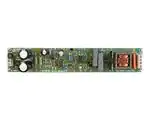
Figure 1. NCP5181 Evaluation Board
WARNING:
BEFORE PLUGGING IN THE EVALUATION BOARD, MAKE SURE THE JUMPER IS IN THE CORRECT POSITION: IF J2
IS USED, THEN Vin MUST BE LOWER THAN 145 Vac.
© Semiconductor Components Industries, LLC, 2012
October, 2012 − Rev. 1
1
Publication Order Number:
EVBUM2141/D
�NCP5181BAL36WEVB
DRV_HI
(5 V/div)
Dead time 260ns
DRV_LO
(5 V/div)
Time
(400 ns/div)
Figure 2. Dead Time Between the High and Low Side Driver
IN_HI
(10 V/div)
DRV_HI
(10 V/div)
IN_LO
(10 V/div)
DRV_LO
(10 V/div)
Time
(4 μs/div)
Figure 3. Input Output Timing Diagram
Tube
Voltage
(100 V/div)
Tube
current
(0.5 V/div)
Tube
Power
(50 W/div)
TubeAverage
power = 32 W
Figure 4. Tube Signals
http://onsemi.com
2
�http://onsemi.com
C16
NC
R10
33k
Figure 5. Evaluation Board Schematic
5
2
4
R15
22k
5V1
D4
CVolt
TRIG
R
U1
TLC555C
F1
T500 mA GND
C11
10nF
GND
Q3
BC547B
R11
47k
GND
C10
220pF
C9
220pF
VCC
CON2
1
2
8
VCC
GND
3
4
DIS
Q
C17
100 uF
R16
68k
27k
R12
6
7
3
GND
GND
VCC
R13
15k
VCC
GND
C12
18pF
GND
Q4
BC547B
C13
18pF
R3
82k
2W
GND
1N4148
D2
R2 82k
C1
47 uF
400 V
SerieM Panasonic
C1
47 uF
400 V
SerieM Panasonic
C3
R1
220uF 12k
GND
D1
15V
1.3W
VCC
DF06
1
PT1
J2
US−jumper
3
THR
GND
1
2
1
J1
2
3
2
1
5
1N4936
D5
U2
NCP5181
GND
IN_LO
IN_HI
VCC
D3
4
6
7
8
R5
10R
GND
D6
1N4936
C14
220pF/400V
DRV_LO
Bridge
DRV_HI
VBOOT
1N4936
C5
100nF
GND
C4
4.7uF
GND
GND
R4
82k
2W
GND
R14
390k
R9
10k
R7
10R
C6
R6 R8
100nF
10R 10k
GND
Q2
IRF840LC
1.4mH
L1
Q1
IRF840LC
6.8nF
1kV
C15
BALLAST
B1
GND
C8
220nF
400V
C7
220nF
400V
NCP5181BAL36WEVB
�NCP5181BAL36WEVB
Figure 6. PCB Printout: Top and Bottom View
http://onsemi.com
4
�NCP5181BAL36WEVB
TEST PROCEDURE
A
A
Vac
V
RLoad
200 W
V
J2 Jumper
Figure 7. Test Setup Connection
Table 1. REQUIRED EQUIPMENT
AC Power Source can be able to deliver 230 Vrms or 110 Vrms
Two Volt-meters
Two Ampere-meters
1 Resistive Load: 200 W/50 W
One NCP5181 Evaluation Board
−
• Voltmeter and Ampmeter on the Load
• Load on the Output
Test Procedure
1. First of all check if you need jumper #2 (J2 on the
board close the diode bridge). This jumper must be
removed for use with European mains (230 Vac
input voltage), and must be in place when using
US mains (110 Vac). This jumper is used to build a
voltage doubler just after the bridge diode in case
one is using US mains input voltage range.
2. Connect the test setup as shown in Figure 7:
• AC Source
3. Apply 230 Vac for European mains or 110 Vac for
US mains on the input connector.
4. Check ILoad and VLoad with the appropriate value
in the table below.
5. If you get the correct output and input voltage, you
can then connect a 36 W fluorescent tube on the
output (see Figure 8).
Table 2. TEST RESULTS
Input Mains
J2
Vin (Vrms)
Iin (Arms)
VLoad (Vrms)
ILoad (Arms)
European
Removed
230 V
278 mA
303 V
370 mA
US
Yes → Max Input Voltage: 132 Vrms
110 V
514 mA
263 V
340 mA
Input Connection
A
Vac
36 W
Tube
V
Output Connection
Figure 8. Ballast Connection
http://onsemi.com
5
�NCP5181BAL36WEVB
Table 3. BILL OF MATERIAL FOR THE NCP5181 EVALUATION BOARD
Designator
Qty.
Description
Value
Tolerance
Footprint
Manufacturer
Manufacturer
Part Number
Substitution
Allowed
Lead
Free
U2
1
NCP5181
NA
NA
DIP8
ON Semiconductor
NCP5181PG
No
Yes
U1
1
CMOS IC
Analog/Timer
NA
DIP8
Texas Instruments
TLC555CP
Yes
No
C1, C2
2
Electrolytic Capacitor
47 mF, 400 V
20%
Radial
Panasonic
ECA2GM470
Yes
No
C3
1
Electrolytic Capacitor
220 mF, 16 V
20%
Radial
Panasonic
ECA1CM221
Yes
No
C4
1
Electrolytic Capacitor
4.7 mF, 63 V
20%
Radial
Panasonic
EEUEB1J4R7
Yes
No
C5, C6
2
Capacitor
100 nF, 50 V
10%
Radial
Murata
RPER71H104K2M1A05U
Yes
No
C7, C8
2
Capacitor
220 nF, 400 V
10%
Radial
Vishay
MKT1822422405
Yes
No
C9, C10
2
Capacitor
220 nF, 100 V
5%
Radial
Murata
RPE5C2A221J2M1Z05A
Yes
No
C11
1
Capacitor
10 nF, 100 V
10%
Radial
Murata
RPER72A103K2M1B05A
Yes
No
C12, C13
2
Capacitor
18 pF, 100 V
2%
Radial
Vishay
2252 586 20154
Yes
Yes
C14
1
Capacitor
220 pF, 400 V
10%
Radial
Panasonic
ECKATS221KB
Yes
No
C15
1
Capacitor
6.8 nF, 1600 V
5%
Radial
Vishay
2222 375 30682
Yes
No
C16
1
Capacitor
NC
−
Radial
−
−
−
−
C17
1
Electrolytic Capacitor
100 mF, 16 V
20%
Radial
Panasonic
ECA1CM101
Yes
No
D1
1
Zener Diode
15 V, 1.3 W
5%
Axial
Vishay
BZX85C15
Yes
No
D2
1
High-speed Diode
0.2 A, 75 V
NA
Axial
Philips
Semiconductor
1N4148
Yes
No
D3, D5, D6
3
Rectifier Diode
1 A, 400 V
NA
Axial
ON Semiconductor
1N4936G
Yes
Yes
D4
1
Zener Diode
5.1 V, 1.3 W
5%
Axial
Vishay
BZX85C5V1
Yes
No
F1
1
Fuse
500 mA, 250 V
NA
Radial
Schurter
0034.6612
Yes
No
L1
1
Inductor
1.4 mH
NA
NA
Vogt
53−044
No
No
PT1
1
Diode Bridge
600 V, 1 A
NA
DFM
Vishay
DF06M
Yes
No
R1
1
Resistor
12 kW, 0.33 W
5%
Axial
Vishay
CFA020712K
Yes
No
R2
1
Resistor
82 kW, 0.33 W
5%
Axial
Vishay
CFA020782K
Yes
No
R3, R4
2
Resistor
82 kW, 3 W
5%
Axial
Vishay
CPF382K000JN
Yes
No
R5, R6, R7
3
Resistor
10 W, 0.33 W
5%
Axial
Vishay
CFA020710R
Yes
No
R8, R9
2
Resistor
10 kW, 0.33 W
5%
Axial
Yageo
CFA020710K
Yes
No
R10
1
Resistor
33 kW, 0.33 W
5%
Axial
Vishay
CFA020733K
Yes
No
R11
1
Resistor
47 kW, 0.33 W
5%
Axial
Vishay
CFA020747K
Yes
No
R12
1
Resistor
27 kW, 0.33 W
5%
Axial
Vishay
CFA020727K
Yes
No
R13
1
Resistor
15 kW, 0.33 W
5%
Axial
Vishay
CFA020715K
Yes
No
R14
1
Resistor
390 kW, 0.33 W
5%
Axial
Vishay
CFA0207390K
Yes
No
R15
1
Resistor
22 kW, 0.33 W
5%
Axial
Vishay
CFA020722K
Yes
No
R16
1
Resistor
68 kW, 0.33 W
5%
Axial
Vishay
CFA020768K
Yes
No
Q1, Q2
2
Power MOSFET
N-channel
8 A, 500 V
NA
TO220
International
Rectifier
IRF840LC
Yes
No
Q3, Q4
2
NPN Transistor
100 mA, 45 V
NA
TO−92
ON Semiconductor
BC547BG
Yes
Yes
B1, J1
2
Connector
2/″
NA
5.08 mm
Weidmuller
PM5.08/2/90
(1760510000)
Yes
No
J2
1
Jumper Resistor
0 W, 0.25 W
NA
Axial
Yageo
ZOR−25−B−52
Yes
No
http://onsemi.com
6
�onsemi,
, and other names, marks, and brands are registered and/or common law trademarks of Semiconductor Components Industries, LLC dba “onsemi” or its affiliates
and/or subsidiaries in the United States and/or other countries. onsemi owns the rights to a number of patents, trademarks, copyrights, trade secrets, and other intellectual property. A
listing of onsemi’s product/patent coverage may be accessed at www.onsemi.com/site/pdf/Patent−Marking.pdf. onsemi is an Equal Opportunity/Affirmative Action Employer. This
literature is subject to all applicable copyright laws and is not for resale in any manner.
The evaluation board/kit (research and development board/kit) (hereinafter the “board”) is not a finished product and is not available for sale to consumers. The board is only intended
for research, development, demonstration and evaluation purposes and will only be used in laboratory/development areas by persons with an engineering/technical training and familiar
with the risks associated with handling electrical/mechanical components, systems and subsystems. This person assumes full responsibility/liability for proper and safe handling. Any
other use, resale or redistribution for any other purpose is strictly prohibited.
THE BOARD IS PROVIDED BY ONSEMI TO YOU “AS IS” AND WITHOUT ANY REPRESENTATIONS OR WARRANTIES WHATSOEVER. WITHOUT LIMITING THE FOREGOING,
ONSEMI (AND ITS LICENSORS/SUPPLIERS) HEREBY DISCLAIMS ANY AND ALL REPRESENTATIONS AND WARRANTIES IN RELATION TO THE BOARD, ANY
MODIFICATIONS, OR THIS AGREEMENT, WHETHER EXPRESS, IMPLIED, STATUTORY OR OTHERWISE, INCLUDING WITHOUT LIMITATION ANY AND ALL
REPRESENTATIONS AND WARRANTIES OF MERCHANTABILITY, FITNESS FOR A PARTICULAR PURPOSE, TITLE, NON−INFRINGEMENT, AND THOSE ARISING FROM A
COURSE OF DEALING, TRADE USAGE, TRADE CUSTOM OR TRADE PRACTICE.
onsemi reserves the right to make changes without further notice to any board.
You are responsible for determining whether the board will be suitable for your intended use or application or will achieve your intended results. Prior to using or distributing any systems
that have been evaluated, designed or tested using the board, you agree to test and validate your design to confirm the functionality for your application. Any technical, applications or
design information or advice, quality characterization, reliability data or other services provided by onsemi shall not constitute any representation or warranty by onsemi, and no additional
obligations or liabilities shall arise from onsemi having provided such information or services.
onsemi products including the boards are not designed, intended, or authorized for use in life support systems, or any FDA Class 3 medical devices or medical devices with a similar
or equivalent classification in a foreign jurisdiction, or any devices intended for implantation in the human body. You agree to indemnify, defend and hold harmless onsemi, its directors,
officers, employees, representatives, agents, subsidiaries, affiliates, distributors, and assigns, against any and all liabilities, losses, costs, damages, judgments, and expenses, arising
out of any claim, demand, investigation, lawsuit, regulatory action or cause of action arising out of or associated with any unauthorized use, even if such claim alleges that onsemi was
negligent regarding the design or manufacture of any products and/or the board.
This evaluation board/kit does not fall within the scope of the European Union directives regarding electromagnetic compatibility, restricted substances (RoHS), recycling (WEEE), FCC,
CE or UL, and may not meet the technical requirements of these or other related directives.
FCC WARNING – This evaluation board/kit is intended for use for engineering development, demonstration, or evaluation purposes only and is not considered by onsemi to be a finished
end product fit for general consumer use. It may generate, use, or radiate radio frequency energy and has not been tested for compliance with the limits of computing devices pursuant
to part 15 of FCC rules, which are designed to provide reasonable protection against radio frequency interference. Operation of this equipment may cause interference with radio
communications, in which case the user shall be responsible, at its expense, to take whatever measures may be required to correct this interference.
onsemi does not convey any license under its patent rights nor the rights of others.
LIMITATIONS OF LIABILITY: onsemi shall not be liable for any special, consequential, incidental, indirect or punitive damages, including, but not limited to the costs of requalification,
delay, loss of profits or goodwill, arising out of or in connection with the board, even if onsemi is advised of the possibility of such damages. In no event shall onsemi’s aggregate liability
from any obligation arising out of or in connection with the board, under any theory of liability, exceed the purchase price paid for the board, if any.
The board is provided to you subject to the license and other terms per onsemi’s standard terms and conditions of sale. For more information and documentation, please visit
www.onsemi.com.
PUBLICATION ORDERING INFORMATION
LITERATURE FULFILLMENT:
Email Requests to: orderlit@onsemi.com
onsemi Website: www.onsemi.com
◊
TECHNICAL SUPPORT
North American Technical Support:
Voice Mail: 1 800−282−9855 Toll Free USA/Canada
Phone: 011 421 33 790 2910
www.onsemi.com
1
Europe, Middle East and Africa Technical Support:
Phone: 00421 33 790 2910
For additional information, please contact your local Sales Representative
�


 工商网监
湘ICP备2023018690号
工商网监
湘ICP备2023018690号
