ON Semiconductor
Is Now
To learn more about onsemi™, please visit our website at
www.onsemi.com
onsemi and and other names, marks, and brands are registered and/or common law trademarks of Semiconductor Components Industries, LLC dba “onsemi” or its affiliates and/or
subsidiaries in the United States and/or other countries. onsemi owns the rights to a number of patents, trademarks, copyrights, trade secrets, and other intellectual property. A listing of onsemi
product/patent coverage may be accessed at www.onsemi.com/site/pdf/Patent-Marking.pdf. onsemi reserves the right to make changes at any time to any products or information herein, without
notice. The information herein is provided “as-is” and onsemi makes no warranty, representation or guarantee regarding the accuracy of the information, product features, availability, functionality,
or suitability of its products for any particular purpose, nor does onsemi assume any liability arising out of the application or use of any product or circuit, and specifically disclaims any and all
liability, including without limitation special, consequential or incidental damages. Buyer is responsible for its products and applications using onsemi products, including compliance with all laws,
regulations and safety requirements or standards, regardless of any support or applications information provided by onsemi. “Typical” parameters which may be provided in onsemi data sheets and/
or specifications can and do vary in different applications and actual performance may vary over time. All operating parameters, including “Typicals” must be validated for each customer application
by customer’s technical experts. onsemi does not convey any license under any of its intellectual property rights nor the rights of others. onsemi products are not designed, intended, or authorized
for use as a critical component in life support systems or any FDA Class 3 medical devices or medical devices with a same or similar classification in a foreign jurisdiction or any devices intended for
implantation in the human body. Should Buyer purchase or use onsemi products for any such unintended or unauthorized application, Buyer shall indemnify and hold onsemi and its officers, employees,
subsidiaries, affiliates, and distributors harmless against all claims, costs, damages, and expenses, and reasonable attorney fees arising out of, directly or indirectly, any claim of personal injury or death
associated with such unintended or unauthorized use, even if such claim alleges that onsemi was negligent regarding the design or manufacture of the part. onsemi is an Equal Opportunity/Affirmative
Action Employer. This literature is subject to all applicable copyright laws and is not for resale in any manner. Other names and brands may be claimed as the property of others.
�NCP5386, NCP5386A,
NCP5386B
1/2 Phase Controller for
CPU and Chipset
Applications
The NCP5386 is a one− or two−phase buck controller which
combines differential voltage and current sensing, and adaptive
voltage positioning to power both AMD and Intel processors and
chipsets. Dual−edge pulse−width modulation (PWM) combined with
inductor current sensing reduces system cost by providing the fastest
initial response to transient load events. Dual−edge multi−phase
modulation reduces total bulk and ceramic output capacitance
required to satisfy transient load−line regulation.
A high performance operational error amplifier is provided, which
allows easy compensation of the system. The proprietary method of
Dynamic Reference Injection makes the error amplifier
compensation virtually independent of the system response to VID
changes, eliminating tradeoffs between overshoot and dynamic VID
performance.
Features
• Meets Intel’s VR 10.0 and 11.0, and AMD Specifications
• No load Intel VR Offset of −19 mV (NCP5386), +20 mV
•
•
•
•
•
•
•
•
•
•
•
•
•
•
•
•
•
(NCP5386A), and 0 mV (NCP5386B)
Dual−Edge PWM for Fastest Initial Response to Transient Loading
High Performance Operational Error Amplifier
Supports both VR11 and Legacy Soft−Start Modes
Dynamic Reference Injection (Patent# 7057381)
DAC Range from 0.5 V to 1.6 V
�0.5% System Voltage Accuracy from 1.0 V to 1.6 V
True Differential Remote Voltage Sensing Amplifier
Phase−to−Phase Current Balancing
“Lossless” Differential Inductor Current Sensing
Differential Current Sense Amplifiers for each Phase
Adaptive Voltage Positioning (AVP)
Frequency Range: 100 kHz – 1.0 MHz
OVP with Resettable, 8 Event Delayed Latch
Threshold Sensitive Enable Pin for VTT Sensing
Power Good Output with Internal Delays
Programmable Soft−Start Time
This is a Pb−Free Device*
http://onsemi.com
MARKING
DIAGRAMS
1
1
NCP5386x
AWLYYWWG
32
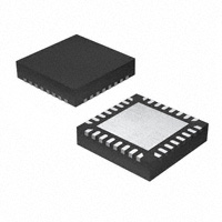
QFN32, 5 x 5*
MN SUFFIX
CASE 485AF
*Pin 33 is the thermal pad on the bottom of the device.
NCP5386 = Specific Device Code
x
= Blank, A or B
A
= Assembly Location
WL
= Wafer Lot
YY
= Year
WW
= Work Week
G
= Pb−Free Package
ORDERING INFORMATION
Package
Shipping†
NCP5386MNR2G*
QFN32
(Pb−Free)
2500 /
Tape & Reel
NCP5386AMNR2G*
QFN32
(Pb−Free)
2500 /
Tape & Reel
NCP5386BMNR2G*
QFN32
(Pb−Free)
2500 /
Tape & Reel
Device
*Temperature Range: 0°C to 85°C
†For information on tape and reel specifications,
including part orientation and tape sizes, please
refer to our Tape and Reel Packaging Specification
Brochure, BRD8011/D.
Applications
• Desktop Processors and Chipsets
• Server Processors and Chipsets
• DDR
*For additional information on our Pb−Free strategy and soldering details, please
download the ON Semiconductor Soldering and Mounting Techniques Reference
Manual, SOLDERRM/D.
© Semiconductor Components Industries, LLC, 2013
July, 2013 − Rev. 3
1
Publication Order Number:
NCP5386/D
�27
26
25
12VMON
G2
28
29
NTC
VR_RDY
30
31
VCC
CS2N
NCP5386/A/B
1/2−Phase Buck Controller
(QFN32)
CS1N
VFB
COMP
DIFFOUT
VDRP
16
9
CS1
AGND Down−Bonded to
Exposed Flag
15
8
DACMODE
VS−
VID7
14
7
13
VID6
VS+
VID5
6
SS
5
NC
VID4
CS2
12
4
VR_FAN
VID3
ILIM
3
DRVON
ROSC
VID2
G1
11
VID1
2
10
1
EN
VID0
32
NCP5386, NCP5386A, NCP5386B
Figure 1. Pin Connections
(Top View)
http://onsemi.com
2
24
23
22
21
20
19
18
17
�NCP5386, NCP5386A, NCP5386B
12 V_FILTER
+5 V
12 V_FILTER
VTT
680 � PULLUPS
C4
+5 V
RVCC
CVCC1
NCP3418B
RNTC1
U1
VCC
VID0
VID0
VID1
VID1
VID2
VID2
VID3
VID3
VID4
VID4
VID5
VID5
VID6
VID6
VID7
VID7
RNTC2
GND
NTC
OD
IN
VR_RDY
VR_FAN
CS1
CS1N
12 V_FILTER
NCP3418
VS−
VCC
VS+
BST
DRVH
OD
SW
DRVL
NCP5386/A/B
IN
CFB1
12 V_FILTER
CS2
CS2N
RISO2
RS1
G2
VR_FAN
RT2
PGND
RT1
CS1
VR_RDY
RISO1
SW
G1
EN
VR_EN
BST
DRVH
DRVL
12VMON
DACMODE
VID_SEL
VCC
PGND
RS2
RFB1
DIFFOUT
CS2
RFB
VFB
RDRP
VDRP
CD1
RD1
CF
RF
DRVON
COMP
ILIM
ROSC SS
CH
RVFB
RLIM1
CSS
RLIM2
RT2 LOCATED NEAR OUTPUT INDUCTORS
VCCP
+
VSSP
CPU/MCH
GND
Figure 2. 2−Phase Application Schematic
http://onsemi.com
3
�NCP5386, NCP5386A, NCP5386B
12 V_FILTER
+5 V
12 V_FILTER
VTT
680 � PULLUPS
+5 V
RVCC
CVCC1
NCP3418B
RNTC1
U1
VCC
VID0
VID0
VID1
VID1
VID2
VID2
VID3
VID3
VID4
VID4
VID5
VID5
VID6
VID6
VID7
VID7
RNTC2
DGND
12VMON
NTC
BST
DRVH
OD
SW
DRVL
IN
PGND
RS1
RT1
CS1
G1
DACMODE
VID_SEL
VCC
CS1
CS1N
EN
VR_EN
VR_RDY
VR_RDY
CS2
VR_FAN
VR_FAN
CS2N
VS−
VS+
RISO1
RISO2
RT2
CFB1
NCP5386/A/B
RFB1
DIFFOUT
RFB
VFB
RDRP
VDRP
CD1
RD1
CF
RF
DRVON
COMP
ILIM
ROSC SS
CH
RVFB
RLIM1
CSS
RLIM2
RT2 LOCATED NEAR OUTPUT INDUCTORS
VCCP
+
VSSP
CPU/MCH
GND
Figure 3. 1−Phase Application Schematic
http://onsemi.com
4
�NCP5386, NCP5386A, NCP5386B
DACMODE
VID0
VID1
VID2
VID3
VID4
VID5
VID6
VID7
NTC
NCP5386/A/B
VR_FAN
VR10/11/AMD
DAC
NTC
+
-
SS
DAC
VS−
-
VS+
+
Diff Amp
DIFFOUT
Fault
1.3 V
+
VFB
-
COMP
VDRP
GND
Error Amp
Droop
Amplifier
+−
1.3 V
CS1
CS1N
+
-
+
-
ENB
G1
+
-
ENB
G2
Gain = 6
CS2
CS2N
+
Gain = 6
OVER
Oscillator
Fault
ROSC
DIFFOUT
+
ILIM
EN
VCC
-
ILimit
+
VCC UVLO
12VMON
+
12VMON UVLO
Figure 4. Simplified Block Diagram
http://onsemi.com
5
Fault Logic
3 Phase
Detect
and
Monitor
Circuits
DRVON
VR_RDY
�NCP5386, NCP5386A, NCP5386B
PIN DESCRIPTIONS
QFN32
Pin No.
Symbol
32, 1 – 7
VID0–VID7
Voltage ID DAC inputs
8
DACMODE
VRM select bit
9
SS
10
ROSC
11
ILIM
Overcurrent shutdown threshold. To program the shutdown threshold, connect this pin to the ROSC pin via a
resistor divider as shown in the Applications Schematics. To disable the over−current feature, connect this pin
directly to the ROSC pin. To guarantee correct operation, this pin should only be connected to the voltage
generated by the ROSC pin; do not connect this pin to any externally generated voltages.
12
NC
Do not connect anything to this pin.
13
VS+
Non−inverting input to the internal differential remote sense amplifier
14
VS−
Inverting input to the internal differential remote sense amplifier
15
DIFFOUT
16
COMP
17
VFB
Error amplifier inverting input. Connect a resistor from this pin to DIFFOUT. The value of this resistor and the
amount of current from the droop resistor (RDRP) will set the amount of output voltage droop (AVP) during
load.
18
VDRP
Current signal output for Adaptive Voltage Positioning (AVP). The voltage of this pin above the 1.3 V internal
offset voltage is proportional to the output current. Connect a resistor from this pin to VFB to set the amount of
AVP current into the feedback resistor (RFB) to produce an output voltage droop. Leave this pin open for no
AVP.
19, 21
CS1N,
CS2N
Inverting input to current sense amplifier.
20, 22
CS1, CS2
23
DRVON
Output to enable Gate Drivers
24, 25
G1, G2
PWM output pulses to gate drivers
26
12VMON
Description
A capacitor from this pin to ground programs the soft−start time.
A resistance from this pin to ground programs the oscillator frequency. Also, this pin supplies an output
voltage of 2 V which may be used to form a voltage divider to the ILIM pin to set the over−current shutdown
threshold as shown in the Applications Schematics.
Output of the differential remote sense amplifier
Output of the error amplifier, and the non−inverting input of the PWM comparators
Non−inverting input to current sense amplifier.
Second UVLO monitor for monitoring the power stage supply rail
27
VCC
28
VR_RDY
Power for the internal control circuits.
29
NTC
Remote temperature sense connection. Connect an NTC thermistor from this pin to GND and a resistor from
this pin to VREF. As the NTC’s temperature increases, the voltage on this pin will decrease.
30
VR_FAN
Open drain output that will be low impedance when the voltage at the NTC pin is above the specified
threshold. This pin will transition to a high impedance state when the voltage at the NTC pin decreases below
the specified threshold. This pin requires an external pull−up resistor.
31
EN
33
GND
Voltage Regulator Ready (Power Good) output. Open drain output that indicates the output is regulating.
Pull this pin high to enable controller. Pull this pin low to disable controller. Either an open−collector output
(with a pull−up resistor) or a logic gate (CMOS or totem−pole output) may be used to drive this pin. A
Low−to−High transition on this pin will initiate a soft start. Connect this pin directly to VREF if the Enable
function is not required. 20 MHz filtering at this pin is required.
Power supply return (QFN Flag)
http://onsemi.com
6
�NCP5386, NCP5386A, NCP5386B
MAXIMUM RATINGS
Electrical Information
Pin Symbol
VMAX (V)
VMIN (V)
ISOURCE (mA)
ISINK (mA)
COMP
5.5
−0.3
10
10
VDRP
5.5
−0.3
5
5
VS+
2.0
GND − 300 mV
1
1
VS−
2.0
GND − 300 mV
1
1
DIFFOUT
5.5
−0.3
20
20
VR_RDY, VR_FAN
5.5
−0.3
N/A
20
VCC
7.0
−0.3
N/A
20
ROSC
5.5
−0.3
1
N/A
DACMODE, EN
3.5
−0.3
0
0
All Other Pins
5.5
−0.3
−
−
Symbol
Value
Unit
R�JA
56
°C/W
Operating Junction Temperature Range (Note 2)
TJ
0 to 125
°C
Operating Ambient Temperature Range
TA
0 to 85
°C
Maximum Storage Temperature Range
TSTG
−55 to +150
°C
Moisture Sensitivity Level, QFN Package
MSL
1
*All signals reference to GND unless otherwise noted.
Thermal Information
Rating
Thermal Characteristic,
QFN Package (Note 1)
Stresses exceeding Maximum Ratings may damage the device. Maximum Ratings are stress ratings only. Functional operation above the
Recommended Operating Conditions is not implied. Extended exposure to stresses above the Recommended Operating Conditions may affect
device reliability.
*The maximum package power dissipation must be observed.
1. JESD 51−5 (1S2P Direct−Attach Method) with 0 Airflow.
2. JESD 51−7 (1S2P Direct−Attach Method) with 0 Airflow.
ELECTRICAL CHARACTERISTICS
(Unless otherwise stated: 0°C < TA < 85°C; 4.75 V < VCC < 5.25 V; All DAC Codes; CVCC = 0.1 �F)
Parameter
Test Conditions
Min
Typ
Max
Units
−200
−
200
nA
Error Amplifier
Input Bias Current
Input Offset Voltage (Note 3)
−1.0
−
1.0
mV
Open Loop DC Gain (Note 3)
CL = 60 pF to GND,
RL = 10 k� to GND
−
100
−
dB
Open Loop Unity Gain Bandwidth
(Note 3)
CL = 60 pF to GND,
RL = 10 k� to GND
−
15
−
MHz
Open Loop Phase Margin (Note 3)
CL = 60 pF to GND,
RL = 10 k� to GND
−
70
−
°
Slew Rate (Note 3)
�VIN = 100 mV, G = −10 V/V,
1.5 V < COMP < 2.5 V,
CL = 60 pF, DC Load = ±125 �A
−
5
−
V/�s
Maximum Output Voltage
10 mV of Overdrive
ISOURCE = 2.0 mA
2.20
VCC −
20 mV
−
V
Minimum Output Voltage
10 mV of Overdrive
ISINK = 2.0 mA
−
0.01
0.5
V
3. Guaranteed by design. Not tested in production.
http://onsemi.com
7
�NCP5386, NCP5386A, NCP5386B
ELECTRICAL CHARACTERISTICS
(Unless otherwise stated: 0°C < TA < 85°C; 4.75 V < VCC < 5.25 V; All DAC Codes; CVCC = 0.1 �F)
Parameter
Test Conditions
Min
Typ
Max
Units
Error Amplifier
Output Source Current (Note 3)
10 mV Input Overdrive
COMP = 2.0 V
2.0
−
−
mA
Output Sink Current (Note 3)
10 mV Input Overdrive
COMP = 1.0 V
2.0
−
−
mA
Differential Summing Amplifier
VS+ Input Resistance
DRVON = Low
DRVON = High
−
−
1.5
17
−
−
k�
VS+ Input Bias Voltage
DRVON = Low
DRVON = High
−
−
0.05
0.65
−
−
V
VS− Bias Current
VS− = 0 V
−
33
−
�A
VS+ Input Voltage Range
0.95 � �DIFFOUT / �VS− � 1.05
0.5 V � DIFFOUT � 2.0 V
−0.3
−
2.0
V
VS− Input Voltage Range
0.95 � �DIFFOUT / �VS− � 1.05
0.5 V � DIFFOUT � 2.0 V
−0.3
−
0.3
V
DC Gain VS+ to DIFFOUT
0 V � DAC − VS+ � 0.3 V
0.99
−
1.01
V/V
DAC Accuracy (measured at VS+)
Closed loop measurement including error
amplifier. (See Figure 20)
1.0 � DAC � 1.6
0.8 � DAC � 1.0
0.5 � DAC � 0.8
−0.5
−5
−8
−
−
−
0.5
5
8
%
mV
mV
−3dB Bandwidth (Note 3)
CL = 80 pF to GND,
RL = 10 k� to GND
−
10
−
MHz
Slew Rate (Note 3)
�VIN = 100 mV,
DIFFOUT = 1.3 V to 1.2 V
−
5.0
−
V/�s
Maximum Output Voltage
VS+ − DAC = 1.0 V
ISOURCE = 2.0 mA
2.0
3.0
−
V
Minimum Output Voltage
VS+ − DAC = −0.8 V
ISINK = 2.0 mA
−
0.01
0.5
V
Output Source Current (Note 3)
VS+ − DAC = 1.0 V
DIFFOUT = 1.0 V
2.0
−
−
mA
Output Sink Current
VS+ − DAC = −0.8 V
DIFFOUT = 1.0 V
2.0
−
−
mA
−
1.30
5.64
5.79
5.95
V/V
−
4
−
MHz
Internal Offset Voltage
VDRP pin offset voltage AND
Error Amp input voltage
V
VDRP Adaptive Voltage−Positioning Amplifier
Current Sense Input to VDRP Gain
−60 mV < (CSx−CSxN) < +60 mV
(Each CS Input Independently)
Current Sense Input to VDRP −3dB
Bandwidth (Note 3)
CL = 30 pF to GND,
RL = 10 k� to GND
VDRP Output Slew Rate (Note 3)
�VIN = 25 mV
1.3 V < VDRP < 1.9 V,
CL = 330 pF to GND,
RL = 1 k� to 10 k� connected to 1.3 V
2.5
−
−
V/�s
VDRP Output Voltage Offset from
Internal Offset Voltage
CSx= CSxN = 1.3 V
−15
−
+15
mV
Maximum VDRP Output Voltage
CSx − CSxN = 0.1 V (all phases),
ISOURCE = 1.0 mA
2.6
3.0
−
V
3. Guaranteed by design. Not tested in production.
http://onsemi.com
8
�NCP5386, NCP5386A, NCP5386B
ELECTRICAL CHARACTERISTICS
(Unless otherwise stated: 0°C < TA < 85°C; 4.75 V < VCC < 5.25 V; All DAC Codes; CVCC = 0.1 �F)
Parameter
Test Conditions
Min
Typ
Max
Units
VDRP Adaptive Voltage−Positioning Amplifier
Minimum VDRP Output Voltage
CSx − CSxN = −0.033 V (all phases),
ISINK = 1.0 mA
−
0.1
0.5
V
Output Source Current (Note 3)
VDRP = 2.0 V
−
1.3
−
mA
Output Sink Current (Note 3)
VDRP = 1.0 V
−
25
−
mA
Current Sense Amplifiers
Input Bias Current
−200
−
200
nA
Common Mode Input Voltage Range
CSx = CSxN = 1.4 V
−0.3
−
2.0
V
Differential Mode Input Voltage Range
(Note 3)
−120
−
120
mV
−1.0
−
1.0
mV
−
6.0
−
V/V
100
−
1000
kHz
196
380
803
−
−
−
226
420
981
kHz
−
−
5
10
−
−
%
1.950
2.010
2.065
V
−
30
40
ns
Propagation Delay (Note 3)
−
20
−
ns
Magnitude of the PWM Ramp
−
1.0
−
V
Input Referred Offset Voltage (Note 3)
CSx = CSxN = 1.0 V
Current Sense Input to PWM Gain
0 V < (CSx − CSxN) < 0.1 V
Oscillator
Switching Frequency Range (Note 3)
Switching Frequency Accuracy
ROSC =
50 k�
25 k�
10 k�
Switching Frequency Tolerance (Note 3)
200 kHz < FSW < 600 kHz
100 kHz < FSW


 工商网监
湘ICP备2023018690号
工商网监
湘ICP备2023018690号
