NCP81063
Synchronous Buck MOSFET
Drivers
The NCP81063 is a high−performance dual MOSFET gate driver
in a small 3 mm x 3 mm package, optimized to drive the gates of both
high−side and low−side power MOSFETs in a synchronous buck
converter. A zero−current detection feature allows for a
high−efficiency solution even at light load conditions. VCC UVLO
ensures the MOSFETs are off when supply voltages are low. A
bi−directional Enable pin provides a fault signal to the controller
when a UVLO fault is detected.
www.onsemi.com
1
DFN8
MN SUFFIX
CASE 506BJ
Features
•
•
•
•
•
•
•
•
•
•
•
•
Space−efficient 3 mm x 3 mm DFN8 Thermally−enhanced Package
VCC Range of 4.5 V to 13.2 V
Integrated Bootstrap Diode
5 V 3−stage PWM input
Zero Current Detect Function Provides Power Saving Operation
During Light Load Conditions
Bi−directional Enable Feature Pulls Enable Pin Low During a
UVLO Fault
Output Disable Control Turns Off Both MOSFETs
VCC Undervoltage Lockout
Adaptive Anti−cross Conduction Circuit Protects Against
Cross−conduction During FET Turn−on and Turn−off
Direct Interface to NCP6151 and Other Compatible PWM
Controllers
Thermally Enhanced Package
These Devices are Pb−Free, Halogen Free/BFR Free and are RoHS
Compliant
• Power Solutions for Notebook and Desktop Systems
October, 2017 − Rev. 1
1
81063
ALYWG
G
81063 = Specific Device Code
A
= Assembly Location
L
= Wafer Lot
Y
= Year
W
= Work Week
G
= Pb−Free Package
(Note: Microdot may be in either location)
ORDERING INFORMATION
Device
NCP81063MNTXG
Package
Shipping†
DFN8
(Pb−Free)
3000 /
Tape & Reel
†For information on tape and reel specifications,
including part orientation and tape sizes, please
refer to our Tape and Reel Packaging Specification
Brochure, BRD8011/D.
Typical Applications
© Semiconductor Components Industries, LLC, 2017
MARKING DIAGRAM
1
Publication Order Number:
NCP81063/D
�NCP81063
BST
DRVH
1
PWM
SW
FLAG
9
EN
GND
VCC
DRVL
(Top View)
Figure 1. Pin Diagram
BST
VCC
DRVH
PWM
Logic
SW
Anti−Cross
Conduction
VCC
DRVL
EN
Fault
ZCD
Detection
UVLO
Pre−OV
Figure 2. Block Diagram
Table 1. Pin Descriptions
Pin No.
Symbol
Description
1
BST
Floating bootstrap supply pin for high side gate driver. Connect the bootstrap capacitor between this pin
and the SW pin.
2
PWM
Control input:
PWM = High → DRVH is high, DRVL is low.
PWM = Mid → Zero current detect enabled. Diode emulation mode.
PWM = Low → DRVH is low, DRVL is high.
3
EN
4
VCC
Power supply input. Connect a bypass capacitor (0.1 mF) from this pin to ground.
5
DRVL
Low side gate drive output. Connect to the gate of low side MOSFET.
6
GND
Bias and reference ground. All signals are referenced to this node (QFN Flag).
3−state input:
EN = High → Driver is enabled.
EN = Low → Driver is disabled.
7
SW
8
DRVH
Switch node. Connect this pin to the source of the high side MOSFET and drain of the low side MOSFET.
High side gate drive output. Connect to the gate of high side MOSFET.
9
FLAG
Thermal flag. There is no electrical connection to the IC. Connect to ground plane.
www.onsemi.com
2
�NCP81063
12V_POWER
TP1
R164
R1
1.02
C4
TP2
0.0
R143 NCP81063 TP3
0.0
TP4
PWM
BST
HG
PWM SW
DRON
EN
LG
C1
4.7uF
C2
4.7uF
+
CE9
390uF
0.0
VREG_SW1_HG
TP5
VCCP
L
VREG_SW1_OUT
235nH
TP6
TP7
Q9
NTMFS4851N
VREG_SW1_LG
Q10
NTMFS4851N
R3
2.2
JP13_ETCH CSN11
PAD
TP8
C5
1uF
C3
4.7uF
R142
GND
VCC
Q1
NTMFS4821N
0.027uF
C6
2700pF
JP14_ETCH CSP11
Figure 3. Application Circuit
Table 2. ABSOLUTE MAXIMUM RATINGS
Pin Symbol
Pin Name
VMAX
VMIN
VCC
Main Supply Voltage Input
15 V
16 V (< 50 ns)
−0.3 V
BST
Bootstrap Supply Voltage
35 V wrt/ GND
40 V ≤ 50 ns wrt/ GND
15 V wrt/ SW
−0.3 V wrt/SW
SW
Switching Node
(Bootstrap Supply Return)
35 V
40 V ≤ 50 ns
−5 V
−10 V (200 ns)
DRVH
High Side Driver Output
BST+0.3 V
SW + 15 V (< 80 ns)
−0.3 V wrt/SW
−2 V (
很抱歉,暂时无法提供与“NCP81063MNTXG”相匹配的价格&库存,您可以联系我们找货
免费人工找货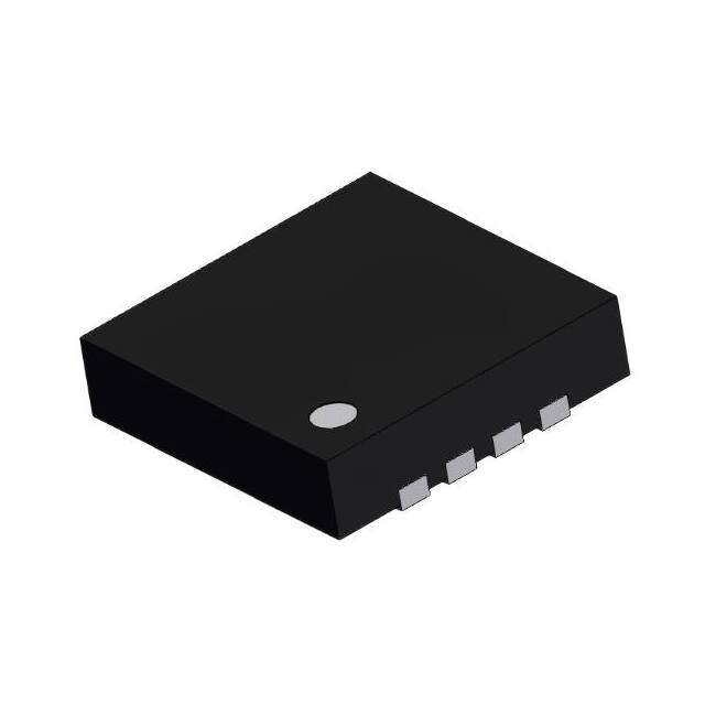


 工商网监
湘ICP备2023018690号
工商网监
湘ICP备2023018690号
