ON Semiconductor
Is Now
To learn more about onsemi™, please visit our website at
www.onsemi.com
onsemi and and other names, marks, and brands are registered and/or common law trademarks of Semiconductor Components Industries, LLC dba “onsemi” or its affiliates and/or
subsidiaries in the United States and/or other countries. onsemi owns the rights to a number of patents, trademarks, copyrights, trade secrets, and other intellectual property. A listing of onsemi
product/patent coverage may be accessed at www.onsemi.com/site/pdf/Patent-Marking.pdf. onsemi reserves the right to make changes at any time to any products or information herein, without
notice. The information herein is provided “as-is” and onsemi makes no warranty, representation or guarantee regarding the accuracy of the information, product features, availability, functionality,
or suitability of its products for any particular purpose, nor does onsemi assume any liability arising out of the application or use of any product or circuit, and specifically disclaims any and all
liability, including without limitation special, consequential or incidental damages. Buyer is responsible for its products and applications using onsemi products, including compliance with all laws,
regulations and safety requirements or standards, regardless of any support or applications information provided by onsemi. “Typical” parameters which may be provided in onsemi data sheets and/
or specifications can and do vary in different applications and actual performance may vary over time. All operating parameters, including “Typicals” must be validated for each customer application
by customer’s technical experts. onsemi does not convey any license under any of its intellectual property rights nor the rights of others. onsemi products are not designed, intended, or authorized
for use as a critical component in life support systems or any FDA Class 3 medical devices or medical devices with a same or similar classification in a foreign jurisdiction or any devices intended for
implantation in the human body. Should Buyer purchase or use onsemi products for any such unintended or unauthorized application, Buyer shall indemnify and hold onsemi and its officers, employees,
subsidiaries, affiliates, and distributors harmless against all claims, costs, damages, and expenses, and reasonable attorney fees arising out of, directly or indirectly, any claim of personal injury or death
associated with such unintended or unauthorized use, even if such claim alleges that onsemi was negligent regarding the design or manufacture of the part. onsemi is an Equal Opportunity/Affirmative
Action Employer. This literature is subject to all applicable copyright laws and is not for resale in any manner. Other names and brands may be claimed as the property of others.
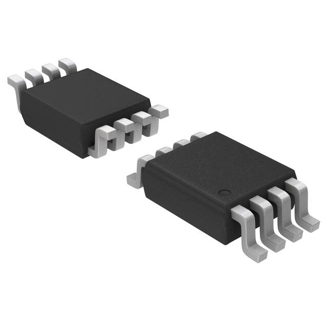
�NLAS323
Dual SPST Analog Switch,
Low Voltage, Single Supply
The NLAS323 is a dual SPST (Single Pole, Single Throw) switch,
similar to 1/2 a standard 4066. The device permits the independent
selection of 2 analog/digital signals. Available in the US8 package.
The use of advanced 0.6 micron CMOS process, improves the RON
resistance considerably compared to older higher voltage
technologies.
www.onsemi.com
MARKING
DIAGRAM
Features
•
•
•
•
•
•
•
•
•
•
•
On Resistance is 20 � Typical at 5.0 V
Matching is < 1.0 � Between Sections
2.0 to 6.0 V Operating Range
Ultra Low < 5.0 pC Charge Injection
Ultra Low Leakage < 1.0 nA at 5.0 V, 25 C
Wide Bandwidth > 200 MHz, −3.0 dB
2000 V ESD (Human Body Model)
Ron Flatness $6.0 � at 5.0 V
US8 Package
Independent, Positive Enable
These Devices are Pb−Free, Halogen Free/BFR Free and are RoHS
Compliant
NO1
1
8
VCC
COM1
2
7
IN1
IN2
3
6
COM2
GND
4
5
NO2
8
US8
US SUFFIX
CASE 493
8
1
A4 MG
G
1
A4
M
G
= Specific Device Code
= Date Code
= Pb−Free Package
(Note: Microdot may be in either location)
PIN ASSIGNMENT
1
NO1
2
COM1
3
IN2
4
GND
5
NO2
6
COM2
7
IN1
8
VCC
FUNCTION TABLE
On/Off
Enable Input
State of
Analog Switch
L
H
Off
On
Figure 1. Pinout
ORDERING INFORMATION
See detailed ordering and shipping information in the package
dimensions section on page 8 of this data sheet.
© Semiconductor Components Industries, LLC, 2015
July, 2015 − Rev. 7
1
Publication Order Number:
NLAS323/D
�NLAS323
MAXIMUM RATINGS
Symbol
Parameter
Value
Unit
VCC
DC Supply Voltage
*0.5 to )7.0
V
VI
DC Input Voltage
*0.5 to )7.0
V
VO
DC Output Voltage
*0.5 to )7.0
V
IIK
DC Input Diode Current
VI < GND
*50
mA
IOK
DC Output Diode Current
VO < GND
*50
mA
IO
DC Output Sink Current
$50
mA
ICC
DC Supply Current per Supply Pin
$100
mA
IGND
DC Ground Current per Ground Pin
$100
mA
TSTG
Storage Temperature Range
*65 to )150
°C
TL
Lead Temperature, 1 mm from Case for 10 Seconds
TJ
Junction Temperature under Bias
�JA
Thermal Resistance
PD
Power Dissipation in Still Air at 85°C
MSL
Moisture Sensitivity
FR
Flammability Rating
VESD
ESD Withstand Voltage
(Note 1)
260
°C
)150
°C
250
°C/W
250
mW
Level 1
Oxygen Index: 28 to 34
UL 94 V−0 @ 0.125 in
Human Body Model (Note 2)
Machine Model (Note 3)
Charged Device Model (Note 4)
> 2000
> 150
N/A
V
Stresses exceeding those listed in the Maximum Ratings table may damage the device. If any of these limits are exceeded, device functionality
should not be assumed, damage may occur and reliability may be affected.
1. Measured with minimum pad spacing on an FR4 board, using 10 mm−by−1 inch, 2−ounce copper trace with no air flow.
2. Tested to EIA/JESD22−A114−A.
3. Tested to EIA/JESD22−A115−A.
4. Tested to JESD22−C101−A.
RECOMMENDED OPERATING CONDITIONS
Symbol
Characteristics
Min
Max
Unit
2.0
5.5
V
VCC
Positive DC Supply Voltage
VIN
Digital Input Voltage (Enable)
GND
5.5
V
VIO
Static or Dynamic Voltage Across an Off Switch
GND
VCC
V
VIS
Analog Input Voltage (NO, COM)
GND
VCC
V
TA
Operating Temperature Range, All Package Types
−55
+125
°C
tr, tf
Input Rise or Fall Time,
(Enable Input)
0
0
100
20
ns/V
Vcc = 3.3 V + 0.3 V
Vcc = 5.0 V + 0.5 V
Functional operation above the stresses listed in the Recommended Operating Ranges is not implied. Extended exposure to stresses beyond
the Recommended Operating Ranges limits may affect device reliability.
90
419,300
47.9
100
178,700
20.4
110
79,600
9.4
120
37,000
4.2
130
17,800
2.0
140
8,900
1.0
TJ = 80°C
117.8
TJ = 90°C
1,032,200
TJ = 100°C
80
TJ = 110°C
Time, Years
TJ = 120°C
Time, Hours
FAILURE RATE OF PLASTIC = CERAMIC
UNTIL INTERMETALLICS OCCUR
TJ = 130°C
Junction
Temperature 5C
NORMALIZED FAILURE RATE
DEVICE JUNCTION TEMPERATURE VERSUS TIME
TO 0.1% BOND FAILURES
1
1
10
100
1000
TIME, YEARS
Figure 2. Failure Rate vs. Time Junction Temperature
www.onsemi.com
2
�NLAS323
DC CHARACTERISTICS − Digital Section (Voltages Referenced to GND)
Guaranteed Max Limit
Symbol
Parameter
Condition
VCC
−55 to 255C


 工商网监
湘ICP备2023018690号
工商网监
湘ICP备2023018690号

