ON Semiconductor
Is Now
To learn more about onsemi™, please visit our website at
www.onsemi.com
onsemi and and other names, marks, and brands are registered and/or common law trademarks of Semiconductor Components Industries, LLC dba “onsemi” or its affiliates and/or
subsidiaries in the United States and/or other countries. onsemi owns the rights to a number of patents, trademarks, copyrights, trade secrets, and other intellectual property. A listing of onsemi
product/patent coverage may be accessed at www.onsemi.com/site/pdf/Patent-Marking.pdf. onsemi reserves the right to make changes at any time to any products or information herein, without
notice. The information herein is provided “as-is” and onsemi makes no warranty, representation or guarantee regarding the accuracy of the information, product features, availability, functionality,
or suitability of its products for any particular purpose, nor does onsemi assume any liability arising out of the application or use of any product or circuit, and specifically disclaims any and all
liability, including without limitation special, consequential or incidental damages. Buyer is responsible for its products and applications using onsemi products, including compliance with all laws,
regulations and safety requirements or standards, regardless of any support or applications information provided by onsemi. “Typical” parameters which may be provided in onsemi data sheets and/
or specifications can and do vary in different applications and actual performance may vary over time. All operating parameters, including “Typicals” must be validated for each customer application
by customer’s technical experts. onsemi does not convey any license under any of its intellectual property rights nor the rights of others. onsemi products are not designed, intended, or authorized
for use as a critical component in life support systems or any FDA Class 3 medical devices or medical devices with a same or similar classification in a foreign jurisdiction or any devices intended for
implantation in the human body. Should Buyer purchase or use onsemi products for any such unintended or unauthorized application, Buyer shall indemnify and hold onsemi and its officers, employees,
subsidiaries, affiliates, and distributors harmless against all claims, costs, damages, and expenses, and reasonable attorney fees arising out of, directly or indirectly, any claim of personal injury or death
associated with such unintended or unauthorized use, even if such claim alleges that onsemi was negligent regarding the design or manufacture of the part. onsemi is an Equal Opportunity/Affirmative
Action Employer. This literature is subject to all applicable copyright laws and is not for resale in any manner. Other names and brands may be claimed as the property of others.
�NLAS5113
1 W RON SPST Switch
The NLAS5113 is an SPST switch designed for very low RON
applications within portable devices. The NLAS5113 operates over a
wide VCC range, 1.65 V to 4.5 V, and maintain a very low RON: 1.3 W
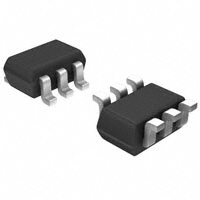
Max @ VCC = 4.2 V. It is available in a choice of two packages: SC88
and UDFN6.
http://onsemi.com
Features
MARKING
DIAGRAMS
•�RON: 1.3 W Max @ VCC = 4.2 V
•�VCC Range: 1.65 V to 4.5 V
•�UDFN6 or SC88 Packages Available
•�These are Pb-Free Devices
UDFN6
CASE 517AA
2M
G
1
Typical Applications
•�Mobile Phones
•�Portable Devices
6
SC-88
CASE 419B
1
AP MG
G
1
XX
M
G
= Device Code
= Date Code
= Pb-Free Package
(Note: Microdot may be in either location)
APPLICATION DIAGRAM
NLAS5113
ORDERING INFORMATION
Device
Package
Shipping†
NLAS5113MUTBG
UDFN6
3000/Tape & Reel
(Pb-Free)
NLAS5113DFT2G
SC-88
3000/Tape & Reel
(Pb-Free)
†For information on tape and reel specifications,
including part orientation and tape sizes, please
refer to our Tape and Reel Packaging Specification
Brochure, BRD8011/D.
©� Semiconductor Components Industries, LLC, 2007
October, 2007 - Rev. 0
1
Publication Order Number:
NLAS5113/D
�NLAS5113
VCC
1
6
COM
COM
1
6
VCC
NO
2
5
N.C.
N.C.
2
5
NO
IN
3
4
GND
GND
3
4
IN
UDFN6
SC88
Figure 1. Functional Block Diagram Pinouts
FUNCTION TABLE
Pin #
Name
Direction
Description
1
VCC
Input
Analog Supply Voltage
IN
NO
2
NO
I/O
Normally Open Signal
Line
0
1
OFF
ON
3
IN
Input
Control Input for
Switch #
4
GND
Input
Ground
5
N.C.
N/A
No Connect
6
COM
I/O
Common Signal Line
http://onsemi.com
2
�NLAS5113
OPERATING CONDITIONS
MAXIMUM RATINGS
Symbol
Pins
VCC
VCC
VIS
NOx, NCx,
COMx
VIN
IN1, IN2
ICC
VCC
IIS_CON
NOx, NCx,
COMx
Analog Signal Continuous Current
±300
Closed Switch
mA
IIS_PK
NOx, NCx,
COMx
Analog Signal Peak Current
±500
10% Duty Cycle
mA
IIN
IN
TSTG
Parameter
Value
Positive DC Supply Voltage
Condition
Unit
-0.5 to 5.5
V
Analog Signal Voltage
-0.5 to VCC + 0.5
V
Control Input Voltage
-0.5 to 6.0
V
50
mA
Positive DC Supply Current
Control Input Current
mA
Storage Temperature Range
°C
-65 to 150
Stresses exceeding Maximum Ratings may damage the device. Maximum Ratings are stress ratings only. Functional operation above the
Recommended Operating Conditions is not implied. Extended exposure to stresses above the Recommended Operating Conditions may affect
device reliability.
RECOMMENDED OPERATING CONDITIONS
Symbol
Pins
Parameter
Value
Unit
VCC
VCC
1.65 to 4.5
V
VIS
NOx, NCx,
COMx
Analog Signal Voltage
0 to VCC
V
VIN
IN1, IN2
Control Input Voltage
0 to VCC
V
Operating Temperature Range
-40 to 85
°C
TA
NOTE:
Positive DC Supply Voltage
Condition
Minimum and maximum values are guaranteed through test or design across the Recommended Operating Conditions, where
applicable. Typical values are listed for guidance only and are based on the particular conditions listed for each section, where
applicable. These conditions are valid for all values found in the characteristics tables unless otherwise specified in the test
conditions.
http://onsemi.com
3
�NLAS5113
DC ELECTRICAL CHARACTERISTICS Typical: T = 25°C; VCC = 3.3 V, RL = 50 W
Symbol
Pins
Parameter
Test Conditions
Min
2.7 V < VCC
2.0
Typ
Max
Unit
VOLTAGE IOUT < 20mA
VIH
INx
Control Input High
VIL
INx
Control Input Low
IIN
INx
Control Input Leakage
0 V < VIN < VCC
INO/NC (OFF)
NCx, NOx
OFF State Leakage
I COM (ON)
COMx
ON State Leakage
ICC
VCC
Quiescent Supply
V
0.8
V
±0.1
±1.0
mA
0 V < VCOM, VNO < VCC
±0.1
±1.0
mA
0 V < VCOM, VNO < VCC
±0.5
±2.0
mA
All Channels ON or OFF;
VIN = VCC or GND, IOUT = 0;
1.0
2.0
mA
Typ
Max
Unit
2.0
1.3
W
CURRENT
ON RESISTANCE ION = -100 mA, VIS = 0 to VCC
Symbol
Pins
Parameter
RON
RFLAT
Test Conditions
VCC
(V)
Min
ON Resistance
2.7
4.2
1.7
1.1
RON Flatness
2.7
4.2
0.4
0.4
W
ESD PROTECTION
Pins
All Pins to Ground
Description
Minimum Voltage
Human Body Model
3 kV
AC ELECTRICAL CHARACTERISTICS Typical: T = 25°C; VCC = 3.3 V, RL = 50 W, CL = 5 pF, f = 1 MHz
Symbol
Parameter
Test Conditions
Min
Typ
Max
Unit
FREQUENCY
BW
-3dB Bandwidth
THD
Total Harmonic Distortion
f = 20 Hz to 20 kHz, 1.0 VPP
457
MHz
0.08
%
TRANSITION TIMES
tON
Turn On Time: COM to NO
7.0
ns
tOFF
Turn Off Time: COM to NO
4.5
ns
-57
dB
OFF ISOLATION VNO or VNC (pk-pk) = 1.0 V
Off Isolation
OIRR
CAPACITANCE
Symbol
Pins
CIN
INx
CON
COFF
Parameter
Control Input
NO to COM Through Switch
NO1, NO
Individual Port
Test Conditions
Min
Typ
Max
Unit
VCC = 0 V
2.8
pF
VCC = VIN = 3.3 V
20
pF
VCC = 3.3 V, VIN = 0 V
14
pF
http://onsemi.com
4
�NLAS5113
PACKAGE DIMENSIONS
UDFN6, 1.2x1.0, 0.4P
CASE 517AA-01
ISSUE B
PIN ONE
REFERENCE
2X
0.10 C
NOTES:
1. DIMENSIONING AND TOLERANCING PER
ASME Y14.5M, 1994.
2. CONTROLLING DIMENSION: MILLIMETERS.
3. DIMENSION b APPLIES TO PLATED TERMINAL
AND IS MEASURED BETWEEN 0.25 AND
0.30 mm FROM TERMINAL.
4. COPLANARITY APPLIES TO THE EXPOSED
PAD AS WELL AS THE TERMINALS.
A
B
D
ÉÉ
ÉÉ
E
DIM
A
A1
A3
b
D
E
e
L
L2
TOP VIEW
2X
0.10 C
(A3)
0.10 C
MILLIMETERS
MIN
MAX
0.45
0.55
0.00
0.05
0.127 REF
0.15
0.25
1.20 BSC
1.00 BSC
0.40 BSC
0.30
0.40
0.40
0.50
A
10X
0.08 C
6X
5X
6X
0.42
C
A1
1
MOUNTING FOOTPRINT*
SEATING
PLANE
SIDE VIEW
0.22
L
3
L2
6X
0.40
PITCH
b
0.10 C A B
0.05 C
6
4
e
NOTE 3
1.07
DIMENSIONS: MILLIMETERS
*For additional information on our Pb-Free strategy and soldering
details, please download the ON Semiconductor Soldering and
Mounting Techniques Reference Manual, SOLDERRM/D.
BOTTOM VIEW
http://onsemi.com
5
�NLAS5113
PACKAGE DIMENSIONS
SC-88/SC70-6/SOT-363
CASE 419B-02
ISSUE W
NOTES:
1. DIMENSIONING AND TOLERANCING PER ANSI
Y14.5M, 1982.
2. CONTROLLING DIMENSION: INCH.
3. 419B-01 OBSOLETE, NEW STANDARD 419B-02.
D
e
6
5
4
1
2
3
HE
DIM
A
A1
A3
b
C
D
E
e
L
HE
-E-
b 6 PL
0.2 (0.008)
M
E
M
MILLIMETERS
MIN
NOM MAX
0.80
0.95
1.10
0.00
0.05
0.10
0.20 REF
0.10
0.21
0.30
0.10
0.14
0.25
1.80
2.00
2.20
1.15
1.25
1.35
0.65 BSC
0.10
0.20
0.30
2.00
2.10
2.20
INCHES
NOM MAX
0.037 0.043
0.002 0.004
0.008 REF
0.004 0.008 0.012
0.004 0.005 0.010
0.070 0.078 0.086
0.045 0.049 0.053
0.026 BSC
0.004 0.008 0.012
0.078 0.082 0.086
MIN
0.031
0.000
SOLDERING FOOTPRINT*
A3
0.50
0.0197
C
A
A1
0.65
0.025
L
0.65
0.025
0.40
0.0157
1.9
0.0748
SCALE 20:1
mm Ǔ
ǒinches
SC-88/SC70-6/SOT-363
*For additional information on our Pb-Free strategy and soldering
details, please download the ON Semiconductor Soldering and
Mounting Techniques Reference Manual, SOLDERRM/D.
ON Semiconductor and
are registered trademarks of Semiconductor Components Industries, LLC (SCILLC). SCILLC reserves the right to make changes without further notice
to any products herein. SCILLC makes no warranty, representation or guarantee regarding the suitability of its products for any particular purpose, nor does SCILLC assume any liability
arising out of the application or use of any product or circuit, and specifically disclaims any and all liability, including without limitation special, consequential or incidental damages.
“Typical” parameters which may be provided in SCILLC data sheets and/or specifications can and do vary in different applications and actual performance may vary over time. All
operating parameters, including “Typicals” must be validated for each customer application by customer's technical experts. SCILLC does not convey any license under its patent rights
nor the rights of others. SCILLC products are not designed, intended, or authorized for use as components in systems intended for surgical implant into the body, or other applications
intended to support or sustain life, or for any other application in which the failure of the SCILLC product could create a situation where personal injury or death may occur. Should
Buyer purchase or use SCILLC products for any such unintended or unauthorized application, Buyer shall indemnify and hold SCILLC and its officers, employees, subsidiaries, affiliates,
and distributors harmless against all claims, costs, damages, and expenses, and reasonable attorney fees arising out of, directly or indirectly, any claim of personal injury or death
associated with such unintended or unauthorized use, even if such claim alleges that SCILLC was negligent regarding the design or manufacture of the part. SCILLC is an Equal
Opportunity/Affirmative Action Employer. This literature is subject to all applicable copyright laws and is not for resale in any manner.
PUBLICATION ORDERING INFORMATION
LITERATURE FULFILLMENT:
Literature Distribution Center for ON Semiconductor
P.O. Box 5163, Denver, Colorado 80217 USA
Phone: 303-675-2175 or 800-344-3860 Toll Free USA/Canada
Fax: 303-675-2176 or 800-344-3867 Toll Free USA/Canada
Email: orderlit@onsemi.com
N. American Technical Support: 800-282-9855 Toll Free
USA/Canada
Europe, Middle East and Africa Technical Support:
Phone: 421 33 790 2910
Japan Customer Focus Center
Phone: 81-3-5773-3850
http://onsemi.com
6
ON Semiconductor Website: www.onsemi.com
Order Literature: http://www.onsemi.com/orderlit
For additional information, please contact your local
Sales Representative
NLAS5113/D
�


 工商网监
湘ICP备2023018690号
工商网监
湘ICP备2023018690号
