NLAS4501
Single SPST Analog Switch
The NLAS4501 is an analog switch manufactured in sub-micron
silicon-gate CMOS technology. It achieves very low RON while
maintaining extremely low power dissipation. The device is a bilateral
switch suitable for switching either analog or digital signals, which may
vary from zero to full supply voltage.
The NLAS4501 is pin-for-pin compatible with the MAX4501. The
NLAS4501 can be used as a direct replacement for the MAX4501 in all
2.0 V to 5.5 V applications where a RON performance improvement
is required.
The Enable pin is compatible with standard CMOS outputs when
supply voltage is nominal 5.0 Volts. It is also over-voltage tolerant,
making it a very useful logic level translator.
•�Guaranteed RON of 32 � at 5.5 V
•�Low Power Dissipation: ICC = 2 �A
•�Provides Voltage translation for many different voltage levels
3.3 to 5.0 V, Enable pin may go as high as +5.5 Volts
1.8 to 3.3 V
1.8 to 2.5 V
•�Improved version of MAX4501 (at any voltage between 2 and 5.5 Volts)
•�Chip Complexity: FETs 11
•�Pb-Free Packages are Available
http://onsemi.com
MARKING
DIAGRAMS
A2d
SC70-5/SC-88A/SOT-353
DF SUFFIX
CASE 419A
5
5
A2d
1
1
SOT23-5/TSOP-5/SC59-5
DT SUFFIX
CASE 483
d = Date Code
COM
1
5
VCC
PIN ASSIGNMENT
2
NO
GND
3
4
ENABLE
1
COM
2
NO
3
GND
4
ENABLE
5
VCC
FUNCTION TABLE
Figure 1. Pinout (Top View)
On/Off Enable Input
State of Analog Switch
L
H
Off
On
ORDERING INFORMATION
See detailed ordering and shipping information on page 7 of
this data sheet.
©� Semiconductor Components Industries, LLC, 2007
October, 2007 - Rev. 5
1
Publication Order Number:
NLAS4501/D
�NLAS4501
MAXIMUM RATINGS
Value
Unit
VCC
Symbol
Positive DC Supply Voltage
Parameter
�0.5 to �7.0
V
VIN
Digital Input Voltage (Enable)
�0.5 to �7.0
V
VIS
Analog Output Voltage (VNO or VCOM)
�0.5 to VCC �0.5
V
IIK
DC Current, Into or Out of Any Pin
�20
mA
TSTG
Storage Temperature Range
�65 to �150
°C
TL
Lead Temperature, 1 mm from Case for 10 Seconds
TJ
Junction Temperature under Bias
�JA
Thermal Resistance
PD
Power Dissipation in Still Air at 85°C
MSL
Moisture Sensitivity
FR
Flammability Rating
VESD
ESD Withstand Voltage
Human Body Model (Note 2)
Machine Model (Note 3)
Charged Device Model (Note 4)
> 2000
> 100
N/A
V
ILatch-Up
Latch-Up Performance
Above VCC and Below GND at 85°C (Note 5)
�300
mA
260
°C
�150
°C
SC70-5/SC-88A (Note 1)
TSOP-5
350
230
°C/W
SC70-5/SC-88A
TSOP-5
150
200
mW
Level 1
Oxygen Index: 30% - 35%
UL-94-VO (0.125 in)
Maximum ratings are those values beyond which device damage can occur. Maximum ratings applied to the device are individual stress limit
values (not normal operating conditions) and are not valid simultaneously. If these limits are exceeded, device functional operation is not implied,
damage may occur and reliability may be affected.
1. Measured with minimum pad spacing on an FR4 board, using 10 mm-by-1 inch, 2-ounce copper trace with no air flow.
2. Tested to EIA/JESD22-A114-A.
3. Tested to EIA/JESD22-A115-A.
4. Tested to JESD22-C101-A.
5. Tested to EIA/JESD78.
RECOMMENDED OPERATING CONDITIONS
Symbol
Characteristics
Min
Max
Unit
VCC
Positive DC Supply Voltage
2.0
5.5
V
VIN
Digital Input Voltage (Enable)
GND
5.5
V
VIO
Static or Dynamic Voltage Across an Off Switch
GND
VCC
V
VIS
Analog Input Voltage (NO, COM)
GND
VCC
V
TA
Operating Temperature Range, All Package Types
-55
+125
°C
tr, tf
Input Rise or Fall Time,
(Enable Input)
0
0
100
20
ns/V
Vcc = 3.3 V + 0.3 V
Vcc = 5.0 V + 0.5 V
90
419,300
47.9
100
178,700
20.4
110
79,600
9.4
120
37,000
4.2
130
17,800
2.0
140
8,900
1.0
TJ = 80°C
117.8
TJ = 90°C
1,032,200
TJ = 100°C
80
TJ = 110°C
Time, Years
TJ = 120°C
Time, Hours
FAILURE RATE OF PLASTIC = CERAMIC
UNTIL INTERMETALLICS OCCUR
TJ = 130°C
Junction
Temperature 5C
NORMALIZED FAILURE RATE
DEVICE JUNCTION TEMPERATURE VERSUS TIME
TO 0.1% BOND FAILURES
1
1
10
100
1000
TIME, YEARS
Figure 2. Failure Rate vs. Time Junction Temperature
http://onsemi.com
2
�NLAS4501
DC CHARACTERISTICS - Digital Section (Voltages Referenced to GND)
-405C to +855C
Symbol
Parameter
Condition
VCC
Min
Typ
Max
Unit
VIH
Minimum High-Level Input Voltage,
Enable Inputs
2.0
3.0
4.5
5.5
1.5
2.1
3.15
3.85
-
-
V
VIL
Maximum Low-Level Input Voltage,
Enable Inputs
2.0
3.0
4.5
5.5
-
-
0.5
0.9
1.35
1.65
V
IIN
Maximum Input Leakage Current, En‐
able Inputs
VIN = 5.5 V or GND
0 V to 5.5 V
-
+0.1
+1.0
�A
ICC
Maximum Quiescent Supply Current
(per package)
Enable and VIS = VCC or
GND
5.5
-
-
1.0
�A
DC ELECTRICAL CHARACTERISTICS - Analog Section
-405C to +855C
Symbol
Parameter
Condition
VCC
Min
Typ
Max
Unit
RON
Maximum ON Resistance
(Figures 8 - 12)
VIN = VIH
VIS = VCC to GND
IIsI =
很抱歉,暂时无法提供与“NLAS4501DFT2G”相匹配的价格&库存,您可以联系我们找货
免费人工找货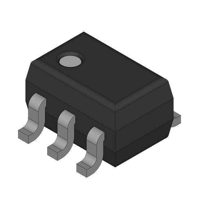


 工商网监
湘ICP备2023018690号
工商网监
湘ICP备2023018690号
