NTST30100CTG,
NTSB30100CT-1G,
NTSJ30100CTG,
NTSB30100CTG
Very Low Forward Voltage
Trench-based Schottky
Rectifier
www.onsemi.com
PIN CONNECTIONS
1
Exceptionally Low VF = 0.455 V at IF = 5 A
2, 4
3
Features
• Fine Lithography Trench−based Schottky Technology for Very Low
•
•
•
•
•
•
Forward Voltage and Low Leakage
Fast Switching with Exceptional Temperature Stability
Low Power Loss and Lower Operating Temperature
Higher Efficiency for Achieving Regulatory Compliance
Low Thermal Resistance
High Surge Capability
These are Pb−Free Devices
4
1
2
3
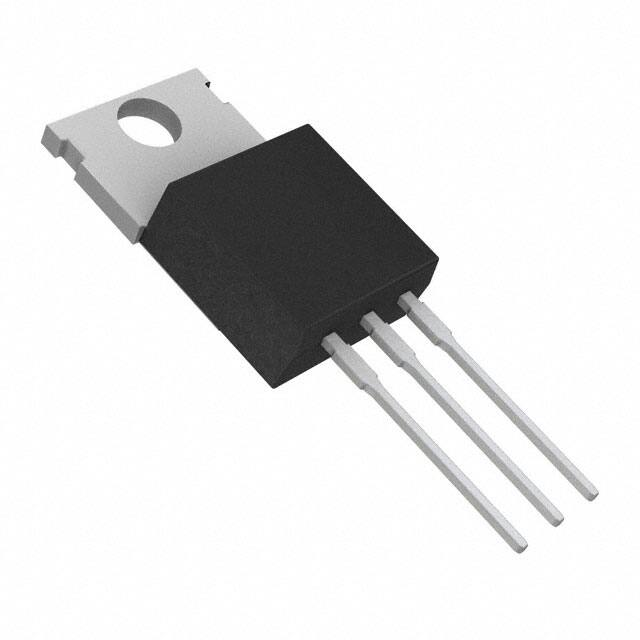
TO−220AB
CASE 221A
STYLE 6
4
12
3
I2PAK
CASE 418D
STYLE 3
Typical Applications
• Switching Power Supplies including Notebook / Netbook Adapters,
•
•
•
•
4
ATX and Flat Panel Display
High Frequency and DC−DC Converters
Freewheeling and OR−ing diodes
Reverse Battery Protection
Instrumentation
1
Mechanical Characteristics
• Case: Epoxy, Molded
• Epoxy Meets Flammability Rating UL 94−0 @ 0.125 in
• Finish: All External Surfaces Corrosion Resistant and Terminal
Leads are Readily Solderable
• Lead Temperature for Soldering Purposes: 260°C Maximum for
TO−220FP
CASE 221AH
2
D2PAK
CASE 418B
3
ORDERING INFORMATION
See detailed ordering and shipping information in the package
dimensions section on page 5 of this data sheet.
10 sec
© Semiconductor Components Industries, LLC, 2016
July, 2016 − Rev. 7
1
Publication Order Number:
NTST30100CT/D
�NTST30100CTG, NTSB30100CT−1G, NTSJ30100CTG, NTSB30100CTG
MAXIMUM RATINGS
Rating
Peak Repetitive Reverse Voltage
Working Peak Reverse Voltage
DC Blocking Voltage
Average Rectified Forward Current
(Rated VR, TC = 115°C)
Symbol
Value
Unit
VRRM
VRWM
VR
100
V
IF(AV)
A
Per device
Per diode
Peak Repetitive Forward Current
(Rated VR, Square Wave, 20 kHz, TC = 110°C)
30
15
IFRM
A
Per device
Per diode
Nonrepetitive Peak Surge Current
(Surge applied at rated load conditions halfwave, single phase, 60 Hz)
60
30
IFSM
160
A
TJ
−40 to +150
°C
Storage Temperature
Tstg
−40 to +150
°C
Voltage Rate of Change (Rated VR)
dv/dt
10,000
V/ms
Operating Junction Temperature
Stresses exceeding those listed in the Maximum Ratings table may damage the device. If any of these limits are exceeded, device functionality
should not be assumed, damage may occur and reliability may be affected.
THERMAL CHARACTERISTICS
Rating
Symbol
NTST30100CTG,
NTSB30100CT−1G
NTSB30100CTG
NTSJ30100CTG
Unit
Maximum Thermal Resistance per Diode
Junction−to−Case
Junction−to−Ambient
RqJC
RqJA
2.5
70
1.14
46.6
4.09
105
°C/W
°C/W
ELECTRICAL CHARACTERISTICS (Per Leg unless otherwise noted)
Rating
Symbol
Maximum Instantaneous Forward Voltage (Note 1)
(IF = 5 A, TJ = 25°C)
(IF = 7.5 A, TJ = 25°C)
(IF = 15 A, TJ = 25°C)
Typ
Max
0.516
0.576
0.734
−
−
0.85
0.455
0.522
0.627
−
−
0.68
vF
(IF = 5 A, TJ = 125°C)
(IF = 7.5 A, TJ = 125°C)
(IF = 15 A, TJ = 125°C)
Maximum Instantaneous Reverse Current (Note 1)
(VR = 70 V, TJ = 25°C)
(VR = 70 V, TJ = 125°C)
V
IR
mA
mA
7.2
8.0
(Rated dc Voltage, TJ = 25°C)
(Rated dc Voltage, TJ = 125°C)
Unit
65
20
500
35
mA
mA
Product parametric performance is indicated in the Electrical Characteristics for the listed test conditions, unless otherwise noted. Product
performance may not be indicated by the Electrical Characteristics if operated under different conditions.
1. Pulse Test: Pulse Width = 300 ms, Duty Cycle v 2.0%
www.onsemi.com
2
�NTST30100CTG, NTSB30100CT−1G, NTSJ30100CTG, NTSB30100CTG
100
100
TA = 150°C
TA = 25°C
I R , REVERSE CURRENT (mA)
i F , INSTANTANEOUS FORWARD CURRENT (AMPS)
TYPICAL CHARACTERISITICS
10
TA = 125°C
1.0
0.1
TA = 150°C
10
TA = 125°C
1.0
0.1
TA = 25°C
0.01
0.001
0
0.2
0.4
0.6
0.8
1.0
1.2
1.4
1.6
1.8
vF, INSTANTANEOUS FORWARD VOLTAGE (VOLTS)
20
30
CJ, JUNCTION CAPACITANCE (pF)
10000
TJ = 25°C
1000
100
10
0.1
100
1
10
VR, REVERSE VOLTAGE (VOLTS)
100
30
RqJC = 1.3°C/W
dc
25
20
15
SQUARE WAVE
10
5
0
0
20
Figure 3. Typical Junction Capacitance
40
60
80
100
120
TC, CASE TEMPERATURE (°C)
140
Figure 4. Current Derating per Leg
60
30
55
50
PF(AV), AVERAGE FORWARD POWER DISSIPATION (W)
IF(AV), AVERAGE FORWARD CURRENT (A)
90
Figure 2. Typical Reverse Current
IF(AV), AVERAGE FORWARD CURRENT (A)
Figure 1. Typical Forward Voltage
50
70
40
60
80
VR, REVERSE VOLTAGE (VOLTS)
RqJC = 1.3°C/W
dc
45
40
35
30
25
SQUARE WAVE
20
15
10
5
IPK/IAV = 10
25
IPK/IAV = 5
IPK/IAV = 20
20
SQUARE
WAVE
15
10
dc
5
TA = 150°C
0
0
0
20
40
60
80
100
120
TC, CASE TEMPERATURE (°C)
0
140
2
4
6
8
10
12
14
16
IF(AV), AVERAGE FORWARD CURRENT (A)
Figure 5. Current Derating
Figure 6. Forward Power Dissipation
www.onsemi.com
3
18
�NTST30100CTG, NTSB30100CT−1G, NTSJ30100CTG, NTSB30100CTG
TYPICAL CHARACTERISITICS
R(t), TYPICAL TRANSIENT THERMAL
RESISTANCE (°C/W)
10
1 50% Duty Cycle
20%
10%
0.1 5%
2%
1%
0.01
0.000001
Single Pulse
0.00001
0.0001
0.001
0.01
0.1
t, Pulse Time (sec)
1
10
100
1000
Figure 7. Typical Transient Thermal Response, Junction−to−Case for NTST30100CT and NTSB30100CT−1G
R(t), TYPICAL TRANSIENT THERMAL
RESISTANCE (°C/W)
10
50% Duty Cycle
1
20%
0.1
10%
5%
2%
1%
0.01
Single Pulse
0.001
0.000001
0.00001
0.0001
0.001
0.01
0.1
1
10
100
1000
100
1000
t, Pulse Time (sec)
R(t), TYPICAL TRANSIENT THERMAL
RESISTANCE (°C/W)
Figure 8. Typical Transient Thermal Response, Junction−to−Case for NTSJ30100CTG
1
50% Duty Cycle
0.1 20%
10%
5%
2%
0.01 1%
0.000001
Single Pulse
0.00001
0.0001
0.001
0.01
0.1
t, Pulse Time (sec)
1
10
Figure 9. Typical Transient Thermal Response, Junction−to−Case for NTSB30100CTG
www.onsemi.com
4
�NTST30100CTG, NTSB30100CT−1G, NTSJ30100CTG, NTSB30100CTG
ORDERING INFORMATION
Package
Shipping
NTST30100CTG
Device
TO−220AB
(Pb−Free)
50 Units / Rail
NTSB30100CT−1G
I2PAK
(Pb−Free)
50 Units / Rail
NTSJ30100CTG
TO−220FP
(Halide−Free)
50 Units / Rail
NTSB30100CTG
D2PAK
(Pb−Free)
50 Units / Rail
NTSB30100CTT4G
D2PAK
(Pb−Free)
800 / Tape & Reel
MARKING DIAGRAMS
AYWW
TS30100Cx
AKA
AYWW
TS30100CG
AKA
TO−220AB
TO−220FP
A
Y
WW
AKA
x
G
H
AYWW
TS30100CG
AKA
I2PAK
= Assembly Location
= Year
= Work Week
= Polarity Designator
= G or H
= Pb−Free Package
= Halide−Free Package
www.onsemi.com
5
AYWW
TS30100CG
AKA
D2PAK
�NTST30100CTG, NTSB30100CT−1G, NTSJ30100CTG, NTSB30100CTG
PACKAGE DIMENSIONS
TO−220
CASE 221A−09
ISSUE AH
−T−
B
SEATING
PLANE
C
F
T
S
4
DIM
A
B
C
D
F
G
H
J
K
L
N
Q
R
S
T
U
V
Z
A
Q
1 2 3
U
H
K
Z
L
R
V
NOTES:
1. DIMENSIONING AND TOLERANCING PER ANSI
Y14.5M, 1982.
2. CONTROLLING DIMENSION: INCH.
3. DIMENSION Z DEFINES A ZONE WHERE ALL
BODY AND LEAD IRREGULARITIES ARE
ALLOWED.
J
G
D
N
INCHES
MIN
MAX
0.570
0.620
0.380
0.415
0.160
0.190
0.025
0.038
0.142
0.161
0.095
0.105
0.110
0.161
0.014
0.024
0.500
0.562
0.045
0.060
0.190
0.210
0.100
0.120
0.080
0.110
0.045
0.055
0.235
0.255
0.000
0.050
0.045
----0.080
STYLE 6:
PIN 1.
2.
3.
4.
MILLIMETERS
MIN
MAX
14.48
15.75
9.66
10.53
4.07
4.83
0.64
0.96
3.61
4.09
2.42
2.66
2.80
4.10
0.36
0.61
12.70
14.27
1.15
1.52
4.83
5.33
2.54
3.04
2.04
2.79
1.15
1.39
5.97
6.47
0.00
1.27
1.15
----2.04
ANODE
CATHODE
ANODE
CATHODE
I2PAK (TO−262)
CASE 418D
ISSUE D
C
E
V
−B−
NOTES:
1. DIMENSIONING AND TOLERANCING PER ANSI
Y14.5M, 1982.
2. CONTROLLING DIMENSION: INCH.
4
A
W
1
2
DIM
A
B
C
D
E
F
G
H
J
K
S
V
W
3
F
−T−
SEATING
PLANE
K
S
J
G
D 3 PL
0.13 (0.005) M T B
H
M
www.onsemi.com
6
INCHES
MIN
MAX
0.335
0.380
0.380
0.406
0.160
0.185
0.026
0.035
0.045
0.055
0.122 REF
0.100 BSC
0.094
0.110
0.013
0.025
0.500
0.562
0.390 REF
0.045
0.070
0.522
0.551
MILLIMETERS
MIN
MAX
8.51
9.65
9.65
10.31
4.06
4.70
0.66
0.89
1.14
1.40
3.10 REF
2.54 BSC
2.39
2.79
0.33
0.64
12.70
14.27
9.90 REF
1.14
1.78
13.25
14.00
�NTST30100CTG, NTSB30100CT−1G, NTSJ30100CTG, NTSB30100CTG
PACKAGE DIMENSIONS
TO−220 FULLPACK, 3−LEAD
CASE 221AH
ISSUE F
A
B
E
A
P
E/2
0.14
Q
D
M
B A
H1
M
A1
C
NOTE 3
1 2 3
L
L1
3X
3X
SEATING
PLANE
c
b
b2
0.25
M
B A
M
C
A2
e
SIDE VIEW
FRONT VIEW
SECTION D−D
A
NOTE 6
NOTE 6
H1
D
D
A
SECTION A−A
ALTERNATE CONSTRUCTION
www.onsemi.com
7
NOTES:
1. DIMENSIONING AND TOLERANCING PER ASME
Y14.5M, 1994.
2. CONTROLLING DIMENSION: MILLIMETERS.
3. CONTOUR UNCONTROLLED IN THIS AREA.
4. DIMENSIONS D AND E DO NOT INCLUDE MOLD FLASH AND GATE
PROTRUSIONS. MOLD FLASH AND GATE PROTRUSIONS NOT TO
EXCEED 0.13 PER SIDE. THESE DIMENSIONS ARE TO BE
MEASURED AT OUTERMOST EXTREME OF THE PLASTIC BODY.
5. DIMENSION b2 DOES NOT INCLUDE DAMBAR PROTRUSION.
LEAD WIDTH INCLUDING PROTRUSION SHALL NOT EXCEED 2.00.
6. CONTOURS AND FEATURES OF THE MOLDED PACKAGE BODY
MAY VARY WITHIN THE ENVELOP DEFINED BY DIMENSIONS A1
AND H1 FOR MANUFACTURING PURPOSES.
DIM
A
A1
A2
b
b2
c
D
E
e
H1
L
L1
P
Q
MILLIMETERS
MIN
MAX
4.30
4.70
2.50
2.90
2.50
2.90
0.54
0.84
1.10
1.40
0.49
0.79
14.70
15.30
9.70
10.30
2.54 BSC
6.60
7.10
12.50
14.73
--2.80
3.00
3.40
2.80
3.20
�NTST30100CTG, NTSB30100CT−1G, NTSJ30100CTG, NTSB30100CTG
PACKAGE DIMENSIONS
D2PAK 3
CASE 418B−04
ISSUE K
NOTES:
1. DIMENSIONING AND TOLERANCING
PER ANSI Y14.5M, 1982.
2. CONTROLLING DIMENSION: INCH.
3. 418B−01 THRU 418B−03 OBSOLETE,
NEW STANDARD 418B−04.
C
E
V
W
−B−
4
DIM
A
B
C
D
E
F
G
H
J
K
L
M
N
P
R
S
V
A
1
2
S
3
−T−
SEATING
PLANE
K
W
J
G
D
H
3 PL
0.13 (0.005)
M
T B
VARIABLE
CONFIGURATION
ZONE
M
N
R
MILLIMETERS
MIN
MAX
8.64
9.65
9.65 10.29
4.06
4.83
0.51
0.89
1.14
1.40
7.87
8.89
2.54 BSC
2.03
2.79
0.46
0.64
2.29
2.79
1.32
1.83
7.11
8.13
5.00 REF
2.00 REF
0.99 REF
14.60 15.88
1.14
1.40
P
U
L
M
INCHES
MIN
MAX
0.340 0.380
0.380 0.405
0.160 0.190
0.020 0.035
0.045 0.055
0.310 0.350
0.100 BSC
0.080
0.110
0.018 0.025
0.090
0.110
0.052 0.072
0.280 0.320
0.197 REF
0.079 REF
0.039 REF
0.575 0.625
0.045 0.055
L
M
L
M
F
F
F
VIEW W−W
1
VIEW W−W
2
VIEW W−W
3
ON Semiconductor and
are trademarks of Semiconductor Components Industries, LLC dba ON Semiconductor or its subsidiaries in the United States and/or other countries.
ON Semiconductor owns the rights to a number of patents, trademarks, copyrights, trade secrets, and other intellectual property. A listing of ON Semiconductor’s product/patent
coverage may be accessed at www.onsemi.com/site/pdf/Patent−Marking.pdf. ON Semiconductor reserves the right to make changes without further notice to any products herein.
ON Semiconductor makes no warranty, representation or guarantee regarding the suitability of its products for any particular purpose, nor does ON Semiconductor assume any liability
arising out of the application or use of any product or circuit, and specifically disclaims any and all liability, including without limitation special, consequential or incidental damages.
Buyer is responsible for its products and applications using ON Semiconductor products, including compliance with all laws, regulations and safety requirements or standards,
regardless of any support or applications information provided by ON Semiconductor. “Typical” parameters which may be provided in ON Semiconductor data sheets and/or
specifications can and do vary in different applications and actual performance may vary over time. All operating parameters, including “Typicals” must be validated for each customer
application by customer’s technical experts. ON Semiconductor does not convey any license under its patent rights nor the rights of others. ON Semiconductor products are not
designed, intended, or authorized for use as a critical component in life support systems or any FDA Class 3 medical devices or medical devices with a same or similar classification
in a foreign jurisdiction or any devices intended for implantation in the human body. Should Buyer purchase or use ON Semiconductor products for any such unintended or unauthorized
application, Buyer shall indemnify and hold ON Semiconductor and its officers, employees, subsidiaries, affiliates, and distributors harmless against all claims, costs, damages, and
expenses, and reasonable attorney fees arising out of, directly or indirectly, any claim of personal injury or death associated with such unintended or unauthorized use, even if such
claim alleges that ON Semiconductor was negligent regarding the design or manufacture of the part. ON Semiconductor is an Equal Opportunity/Affirmative Action Employer. This
literature is subject to all applicable copyright laws and is not for resale in any manner.
PUBLICATION ORDERING INFORMATION
LITERATURE FULFILLMENT:
Literature Distribution Center for ON Semiconductor
19521 E. 32nd Pkwy, Aurora, Colorado 80011 USA
Phone: 303−675−2175 or 800−344−3860 Toll Free USA/Canada
Fax: 303−675−2176 or 800−344−3867 Toll Free USA/Canada
Email: orderlit@onsemi.com
N. American Technical Support: 800−282−9855 Toll Free
USA/Canada
Europe, Middle East and Africa Technical Support:
Phone: 421 33 790 2910
Japan Customer Focus Center
Phone: 81−3−5817−1050
www.onsemi.com
8
ON Semiconductor Website: www.onsemi.com
Order Literature: http://www.onsemi.com/orderlit
For additional information, please contact your local
Sales Representative
NTST30100CT/D
�


 工商网监
湘ICP备2023018690号
工商网监
湘ICP备2023018690号
