Is Now Part of
To learn more about ON Semiconductor, please visit our website at
www.onsemi.com
32�7IQMGSRHYGXSV�ERH�XLI�32�7IQMGSRHYGXSV�PSKS�EVI�XVEHIQEVOW�SJ�7IQMGSRHYGXSV�'SQTSRIRXW�-RHYWXVMIW��00'�HFE�32�7IQMGSRHYGXSV�SV�MXW�WYFWMHMEVMIW�MR�XLI�9RMXIH�7XEXIW�ERH�SV�SXLIV�GSYRXVMIW��32�7IQMGSRHYGXSV�S[RW�XLI�VMKLXW�XS�E�RYQFIV�
SJ�TEXIRXW��XVEHIQEVOW��GST]VMKLXW��XVEHI�WIGVIXW��ERH�SXLIV�MRXIPPIGXYEP�TVSTIVX]��%�PMWXMRK�SJ�32�7IQMGSRHYGXSVvW�TVSHYGX�TEXIRX�GSZIVEKI�QE]�FI�EGGIWWIH�EX�[[[�SRWIQM�GSQ�WMXI�THJ�4EXIRX�1EVOMRK�THJ��32�7IQMGSRHYGXSV�VIWIVZIW�XLI�VMKLX�
XS�QEOI�GLERKIW�[MXLSYX�JYVXLIV�RSXMGI�XS�ER]�TVSHYGXW�LIVIMR��32�7IQMGSRHYGXSV�QEOIW�RS�[EVVERX]��VITVIWIRXEXMSR�SV�KYEVERXII�VIKEVHMRK�XLI�WYMXEFMPMX]�SJ�MXW�TVSHYGXW�JSV�ER]�TEVXMGYPEV�TYVTSWI��RSV�HSIW�32�7IQMGSRHYGXSV�EWWYQI�ER]�PMEFMPMX]�
7IQMGSRHYGXSV�TVSHYGXW��MRGPYHMRK�GSQTPMERGI�[MXL�EPP�PE[W��VIKYPEXMSRW�ERH�WEJIX]�VIUYMVIQIRXW�SV�WXERHEVHW��VIKEVHPIWW�SJ�ER]�WYTTSVX�SV�ETTPMGEXMSRW�MRJSVQEXMSR�TVSZMHIH�F]�32�7IQMGSRHYGXSV��w8]TMGEPx�TEVEQIXIVW�[LMGL�QE]�FI�TVSZMHIH�MR�32�
XIGLRMGEP�I\TIVXW��32�7IQMGSRHYGXSV�HSIW�RSX�GSRZI]�ER]�PMGIRWI�YRHIV�MXW�TEXIRX�VMKLXW�RSV�XLI�VMKLXW�SJ�SXLIVW��32�7IQMGSRHYGXSV�TVSHYGXW�EVI�RSX�HIWMKRIH��MRXIRHIH��SV�EYXLSVM^IH�JSV�YWI�EW�E�GVMXMGEP�GSQTSRIRX�MR�PMJI�WYTTSVX�W]WXIQW�SV�ER]�*(%�
SJ��HMVIGXP]�SV�MRHMVIGXP]��ER]�GPEMQ�SJ�TIVWSREP�MRNYV]�SV�HIEXL�EWWSGMEXIH�[MXL�WYGL�YRMRXIRHIH�SV�YREYXLSVM^IH�YWI��IZIR�MJ�WYGL�GPEMQ�EPPIKIW�XLEX�32�7IQMGSRHYGXSV�[EW�RIKPMKIRX�VIKEVHMRK�XLI�HIWMKR�SV�QERYJEGXYVI�SJ�XLI�TEVX��32�7IQMGSRHYGXSV�
�April 2017
S1AFL - S1MFL
Surface General-Purpose Rectifier
Features
•
•
•
•
•
•
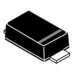
SOD-123F
Ultra Thin Profile – Maximum Height of 1.08 mm
UL Flammability 94V-0 Classification
Glass Passivated Junction
MSL 1
RoHS Compliant / Green Mold Compound
Industrial Device Qualified per AEC-Q101 Standards.
* see authorized use policy
Band Indicates Cathode
Ordering Information
Part Number
Top Mark
Package
Packing Method
S1AFL
1A
SOD-123F
Tape and Reel
S1BFL
1B
SOD-123F
Tape and Reel
S1DFL
1D
SOD-123F
Tape and Reel
S1GFL
1G
SOD-123F
Tape and Reel
S1JFL
1J
SOD-123F
Tape and Reel
S1MFL
1M
SOD-123F
Tape and Reel
Absolute Maximum Ratings
Stresses exceeding the absolute maximum ratings may damage the device. The device may not function or be operable above the recommended operating conditions and stressing the parts to these levels is not recommended. In addition, extended exposure to stresses above the recommended operating conditions may affect device reliability. The
absolute maximum ratings are stress ratings only. Values are at TA = 25°C unless otherwise noted.
Symbol
Value
Parameter
S1AFL S1BFL S1DFL S1GFL S1JFL S1MFL
Unit
VRRM
Recurrent Peak Reverse Voltage
50
100
200
400
600
1000
V
VRMS
RMS Voltage
35
70
140
280
420
700
V
50
100
200
400
600
1000
V
VDC
IF(AV)
IFSM
DC Blocking Voltage
Average Forward Current
(1)
Peak One Cycle Surge Forward Current
(Non-Repetitive) at 60Hz
TJ, TSTG Operating and Storage Temperature Range
1
A
30
A
-50 to +150
C
Note:
1. Pulse test: 300 s pulse width, 1% duty cycle
© 2017 Semiconductor Components Industries, LLC
S1AFL - S1MFL ’Rev. 1.2
1
www.fairchildsemi.com
www.onsemi.com
�Thermal Characteristics(2)
Values are at TA = 25°C unless otherwise noted.
Symbol
R
Parameter
Value
JL
Typical Thermal Characteristics, Junction-to-Lead
JA
Typical Thermal Resistance, Junction-to-Ambient
(3)
Unit
25
C/W
140
C/W
Note:
2. Per JESD51-3 recommended thermal test board. Device mounted on FR-4 PCB, board size = 76.2 mm x 114.3 mm.
3. Thermocouple soldered at cathode lead.
Electrical Characteristics
Values are at TA = 25°C unless otherwise noted.
Symbol
Parameter
Conditions
VF
Forward Voltage
IF = 1 A
IR
Reverse Current
VR = VDC
Trr
Reverse Recovery Time
IF = 0.5 A, IR = 1 A, Irr = 0.25 A
CJ
Junction Capacitance
VR = 4 V, f = 1.0 MHz
© 2017 Semiconductor Components Industries, LLC
S1AFL - S1MFL ’Rev. 1.2
2
Min.
Typ.
Max.
Unit
1.1
V
TA = 25°C
1
TA = 125°C
50
1.304
4
2
A
s
pF
www.fairchildsemi.com
www.onsemi.com
�Typical Performance Characteristics
Figure 1. Forward Current Derating Curve
Figure 2. Typical Instantaneous Forward
Characteristics
Figure 3. Typical Reverse Characteristic
Figure 4. Typical Junction Capacitance
10
1
o
TA= 150 C
o
TA= 125 C
0.1
o
TA= 75 C
o
0.01
TA= 100 C
o
TA= 25 C
1E-3
0.2
0.4
0.6
0.8
1.0
1.2
Forward Voltage, VF [V]
Figure 5. Maximum Non-Repetitive Surge Current
© 2017 Semiconductor Components Industries, LLC
S1AFL - S1MFL ’Rev. 1.2
Figure 6. Typical Forward Characteristics
3
www.fairchildsemi.com
www.onsemi.com
�Physical Dimensions
Figure 7. 2-LEAD, SOD123F, NON-JEDEC, FLAT TERMINAL
© 2017 Semiconductor Components Industries, LLC
S1AFL - S1MFL ’Rev. 1.2
4
www.fairchildsemi.com
www.onsemi.com
�ON Semiconductor and
are trademarks of Semiconductor Components Industries, LLC dba ON Semiconductor or its subsidiaries in the United States and/or other countries.
ON Semiconductor owns the rights to a number of patents, trademarks, copyrights, trade secrets, and other intellectual property. A listing of ON Semiconductor’s product/patent
coverage may be accessed at www.onsemi.com/site/pdf/Patent Marking.pdf. ON Semiconductor reserves the right to make changes without further notice to any products herein.
ON Semiconductor makes no warranty, representation or guarantee regarding the suitability of its products for any particular purpose, nor does ON Semiconductor assume any liability
arising out of the application or use of any product or circuit, and specifically disclaims any and all liability, including without limitation special, consequential or incidental damages.
Buyer is responsible for its products and applications using ON Semiconductor products, including compliance with all laws, regulations and safety requirements or standards,
regardless of any support or applications information provided by ON Semiconductor. “Typical” parameters which may be provided in ON Semiconductor data sheets and/or
specifications can and do vary in different applications and actual performance may vary over time. All operating parameters, including “Typicals” must be validated for each customer
application by customer’s technical experts. ON Semiconductor does not convey any license under its patent rights nor the rights of others. ON Semiconductor products are not
designed, intended, or authorized for use as a critical component in life support systems or any FDA Class 3 medical devices or medical devices with a same or similar classification
in a foreign jurisdiction or any devices intended for implantation in the human body. Should Buyer purchase or use ON Semiconductor products for any such unintended or unauthorized
application, Buyer shall indemnify and hold ON Semiconductor and its officers, employees, subsidiaries, affiliates, and distributors harmless against all claims, costs, damages, and
expenses, and reasonable attorney fees arising out of, directly or indirectly, any claim of personal injury or death associated with such unintended or unauthorized use, even if such
claim alleges that ON Semiconductor was negligent regarding the design or manufacture of the part. ON Semiconductor is an Equal Opportunity/Affirmative Action Employer. This
literature is subject to all applicable copyright laws and is not for resale in any manner.
PUBLICATION ORDERING INFORMATION
LITERATURE FULFILLMENT:
Literature Distribution Center for ON Semiconductor
19521 E. 32nd Pkwy, Aurora, Colorado 80011 USA
Phone: 303 675 2175 or 800 344 3860 Toll Free USA/Canada
Fax: 303 675 2176 or 800 344 3867 Toll Free USA/Canada
Email: orderlit@onsemi.com
Semiconductor Components Industries, LLC
N. American Technical Support: 800 282 9855 Toll Free
USA/Canada
Europe, Middle East and Africa Technical Support:
Phone: 421 33 790 2910
Japan Customer Focus Center
Phone: 81 3 5817 1050
www.onsemi.com
1
ON Semiconductor Website: www.onsemi.com
Order Literature: http://www.onsemi.com/orderlit
For additional information, please contact your local
Sales Representative
www.onsemi.com
�


 工商网监
湘ICP备2023018690号
工商网监
湘ICP备2023018690号
