STK404-070NGEVB,
STK404-120NGEVB,
STK404-140NGEVB
STK404-000N Series
Evaluation Board
User's Manual
http://onsemi.com
EVAL BOARD USER’S MANUAL
Thick-Film Hybrid IC for use used in from 60 W to 180 W
× 1ch class AB audio power amplifiers.
This Evaluation Board User’s Manual describes the set-up
and use of the STK404−000N Series Evaluation Board for
SANYO Semiconductor (An ON Semiconductor Company).
Thick-Film Hybrid IC for use in from 60 W to 180 W
× 1ch class AB audio power amplifiers devices
STK404-070N-E, STK404-120N-E and STK404-140N-E.
For data sheets and additional on these devices, please
visit the ON Semiconductor website at www.onsemi.com.
Figure 1. STK404−000N Series Evaluation Board
EVALUATION BOARD FOR STK404−070N, −120N, −140N
(100 mm × 70 mm × 1.6 mm,
Phenol 1-layer Board)
(100 mm × 70 mm × 1.6 mm,
Phenol 1-layer Board)
(100 mm × 70 mm × 1.6 mm,
Phenol 1-layer Board)
Figure 2. STK404−070NGEVB
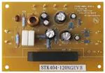
Figure 3. STK404−120NGEVB
Figure 4. STK404−140NGEVB
Table 1. SELECTION GUIDE
STK404−070N−E
STK404−120N−E
STK404−140N−E
Output1 (10%/1 kHz)
60 W × 1ch
120 W × 1ch
180 W × 1ch
Output2 (1%/20 Hz to 20 kHz)
40 W × 1ch
80 W × 1ch
120 W × 1ch
Maximum Rating VCC max (no sig.)
±46 V
±65 V
±78 V
Maximum Rating VCC (6 W)
±39 V
±59 V
±73 V
Recommended Operating VCC (6 W)
±30 V
±41 V
±51 V
44.0 × 25.6 × 8.5 (mm)
46.6 × 25.5 × 8.5 (mm)
59.2 × 25.5 × 8.5 (mm)
Package Size
© Semiconductor Components Industries, LLC, 2013
June, 2013 − Rev. 0
1
Publication Order Number:
EVBUM2197/D
�STK404−070NGEVB, STK404−120NGEVB, STK404−140NGEVB
Constant-voltage
Supply
Signal
Output Load (RL = 6 W)
CH1
GND
OSC Output (600 W)
CH1
Figure 5. Characteristics Confirmation
+VCC
10,000 mF
500 W
+
500 W
−VCC
Specified Transformer Power Supply
STK404-070N-E
(Equivalent to MG-200)
STK404-120N-E/140N-E
(Equivalent to MG-250)
+
10,000 mF
Constant-voltage Supply
Signal
Speaker
(CH1)
Music Source
(CH1)
GND
Figure 6. Sound Quality Configuration, Load Short-circuit Test, Noise Examination
http://onsemi.com
2
�STK404−070NGEVB, STK404−120NGEVB, STK404−140NGEVB
STK404−000NSR PCB PARTS LIST
Table 2. PCB NAME: STK404−000SR GEVB − A
Type (IC1)
STK404−070N−E
STK404−120N−E
STK404−140N−E
Position of (1)pin
Third from the Right End
Second from the Right End
The Right End
1 kW
←
←
R2
56 kW
←
←
R3
1.8 kW
←
←
R4
100 W/1 W
←
←
R5
56 kW
←
←
R6
10 kW/1 W
4.7 kW/1 W
5.1 kW/1 W
R7
10 kW/1 W
4.7 kW/1 W
5.1 kW/1 W
R8
0.22 W/5 W
←
←
R9
−
0.22 W/5 W
←
R10
4.7 W/1 W
←
←
R11
4.7 W/1 W
←
←
C1
470 pF
←
←
C2
2.2 mF/50 V
←
←
C3
10 mF/50 V
←
←
C4
100 mF/100 V
←
←
C5
5 pF
←
←
C6
100 mF/50 V
←
←
C7
47 mF/100 V
←
←
C8
10 mF/100 V
←
←
C9
10 mF/100 V
←
←
C10
0.1 mF
←
←
D1
200 V/0.5 A
Short
Short
L1
2.2 mH
←
←
J1
15 mm
←
←
J2
10 mm
←
←
Location
R1
http://onsemi.com
3
�STK404−070NGEVB, STK404−120NGEVB, STK404−140NGEVB
TEST CIRCUITS
STK404−070N−E
1
R1
IN
C1
2
4
5
C4
+
C2
3
R3
R2
R4
7
D1
+
+
C3
6
+
8
9
10
+
C8
+
R8
C9
R6
C6
R7
C7
+12V
+VCC
−VCC
+
C5
R10
L1
R5
OUT
C10
RL
R11
Figure 7. STK404−070N−E Test Circuit
STK404−120N−E
1
2
R1
IN
3
+
C2
C1
4
C3
6
C4
R3
R2
5
7
R4
9
C8
+
+
8
R6
+
10
11
+
+
12
R8
C9
R9
C6
+ R7
C5
C7
R10
L1
R5
+12V
+VCC
−VCC
OUT
C10
RL
R11
Figure 8. STK404−120N−E Test Circuit
STK404−140N−E
1
IN
2
R1
C1
3
4
+
C2
C3
6
C4
R3
R2
5
+
7
8
9
10
11
12
+
R4
+
R6
+
C8
+
C9
13
R8
+12V
+VCC
−VCC
C6
+ R7
C5
C7
R10
L1
R5
http://onsemi.com
4
OUT
C10
R11
Figure 9. STK404−140N−E Test Circuit
R9
RL
�STK404−070NGEVB, STK404−120NGEVB, STK404−140NGEVB
SUBSTRATE SPECIFICATIONS
(Substrate Recommended for Operation of STK404-070N/120N/140N)
Size:
100 mm × 70 mm × 1.6 mm, Phenol 1-layer Board
Material: Phenol
Copper Side (35 m)
PCB LAYOUT EXAMPLE
Figure 10. Top View
Figure 11. Top View
http://onsemi.com
5
�STK404−070NGEVB, STK404−120NGEVB, STK404−140NGEVB
CHARACTERISTIC OF EVALUATION BOARD − STK404−070N−E
10
1
60
VCC = ±30 V
RL = 6 W
1ch Drive
VG = 30 dB
Rg = 600 W
TC = 25°C
Total Device Power Dissipation, Pd (W)
Total Harmonic Distortion THD (%)
100
f = 20 kHz
0.1
f = 1 kHz
0.01
0.001
0.1
1
10
VCC = ±30 V
f = 1 kHz
RL = 6 W
1ch Drive
VG = 30 dB
Rg = 600 W
TC = 25°C
50
40
30
20
10
0
0.1
100
Output Power per Channel, Po/ch (W)
1
1000
Figure 13. Pd vs. Po
120
120
f = 1 kHz
RL = 6 W
1ch Drive
VG = 30 dB
Rg = 600 W
TC = 25°C
110
100
90
80
70
THD = 10%
(f = 1 kHz)
Output Power per Channel, Po/ch (W)
Output Power per Channel, Po/ch (W)
100
Output Power per Channel, Po/ch (W)
Figure 12. THD vs. Po
THD = 0.4%
(f = 1 kHz)
60
50
40
30
20
10
0
10
110
100
90
THD = 10%
80
70
THD = 0.4%
60
50
VCC = ±30 V
RL = 6 W
1ch Drive
VG = 30 dB
Rg = 600 W
TC = 25°C
40
30
20
10
20
22
24
26
28
30
32
34
36
38
0
40
10
Supply Voltage, VCC (±V)
100
1000
10000
Frequency, f (Hz)
Figure 14. Po vs. VCC
Figure 15. Po vs. f
http://onsemi.com
6
100000
�STK404−070NGEVB, STK404−120NGEVB, STK404−140NGEVB
CHARACTERISTIC OF EVALUATION BOARD − STK404−120N−E
10
1
100
VCC = ±41 V
RL = 6 W
1ch Drive
VG = 30 dB
Rg = 600 W
TC = 25°C
Total Device Power Dissipation, Pd (W)
Total Harmonic Distortion THD (%)
100
f = 20 kHz
0.1
f = 1 kHz
0.01
0.001
0.1
1
10
100
1000
VCC = ±41 V
f = 1 kHz
RL = 6 W
1ch Drive
VG = 30 dB
Rg = 600 W
TC = 25°C
90
80
70
60
50
40
30
20
10
0
0.1
Output Power per Channel, Po/ch (W)
1
THD = 10%
Output Power per Channel, Po/ch (W)
Output Power per Channel, Po/ch (W)
200
THD = 0.4%
100
0
20
30
40
50
1000
Figure 17. Pd vs. Po
300
f = 1 kHz
RL = 6 W
1ch Drive
VG = 30 dB
Rg = 600 W
TC = 25°C
100
Output Power per Channel, Po/ch (W)
Figure 16. THD vs. Po
300
10
60
200
THD = 10%
THD = 1%
100
0
70
VCC = ±41 V
RL = 6 W
1ch Drive
VG = 30 dB
Rg = 600 W
TC = 25°C
10
Supply Voltage, VCC (±V)
100
1000
10000
Frequency, f (Hz)
Figure 18. Po vs. VCC
Figure 19. Po vs. f
http://onsemi.com
7
100000
�STK404−070NGEVB, STK404−120NGEVB, STK404−140NGEVB
CHARACTERISTIC OF EVALUATION BOARD − STK404−140N−E
10
1
160
VCC = ±51 V
RL = 6 W
1ch Drive
VG = 30 dB
Rg = 600 W
TC = 25°C
Total Device Power Dissipation, Pd (W)
Total Harmonic Distortion THD (%)
100
f = 20 kHz
0.1
f = 1 kHz
0.01
0.001
0.1
1
10
100
1000
VCC = ±51 V
f = 1 kHz
RL = 6 W
1ch Drive
VG = 30 dB
Rg = 600 W
TC = 25°C
140
120
100
80
60
40
20
0
0.1
Output Power per Channel, Po/ch (W)
1
300
f = 1 kHz
RL = 6 W
1ch Drive
VG = 30 dB
Rg = 600 W
TC = 25°C
THD = 10%
THD = 0.4%
100
0
20
30
1000
Figure 21. Pd vs. Po
Output Power per Channel, Po/ch (W)
Output Power per Channel, Po/ch (W)
200
100
Output Power per Channel, Po/ch (W)
Figure 20. THD vs. Po
300
10
40
50
60
THD = 10%
200
VCC = ±51 V
RL = 6 W
1ch Drive
VG = 30 dB
Rg = 600 W
TC = 25°C
100
0
70
THD = 1%
10
Supply Voltage, VCC (±V)
100
1000
10000
Frequency, f (Hz)
Figure 22. Po vs. VCC
Figure 23. Po vs. f
http://onsemi.com
8
100000
�STK404−070NGEVB, STK404−120NGEVB, STK404−140NGEVB
STAND−BY CONTROL & MUTE CONTROL APPLICATION
STK404−070N−E
STK404−120N−E
STK404−140N−E
1
2
3
4
5
6
7
8
9
10
1
2
3
4
5
6
7
8
9
10
11
12
2
3
4
5
6
7
8
9
10
11
12
13
1
+
IN
10kW
+
+
+
10kW
+
+
2.2kW
+12V
+VCC
−VCC
+
Mute Control
H:Signal Mute
L:Normal
OUT
tdr > 1s
SB1
5V
Mute
10kW
10kW
5V
+12V
SB2
SB1
ST−BYMUTE PLAY MUTE ST−BY
10kW
10kW
10kW
10kW
5V
SB2
10kW
10kW
tdf > 100ms
+VCC
6.8kW
Vz=13V
12V Regulator
Stand−by Control
H:Operation Mode
L:Stand−by Mode
Figure 24. STK404−000−Ese Stand-by Control & Mute Control Application
THERMAL SHUT DOWN APPLICATION
STK404−070N−E
No Thermal Sensor
Thermal Sensor
STK404−120N−E
1
Shutdown Signal
2
3
4
5
6
7
8
9
10
11
12
4
5
6
7
8
9
10
11
12
13
+12V
Thermal Sensor
STK404−140N−E
Shutdown Signal
1
2
3
+12V
Figure 25. STK404−000−Esr Thermal Shut Down Application
http://onsemi.com
9
�STK404−070NGEVB, STK404−120NGEVB, STK404−140NGEVB
THERMAL SENSOR CHARACTERISTIC
STK404−120N−E
100k
Reference
7
7
5
5
3
3
2
2
10k
10k
7
7
Resistance, Rp (W)
Resistance, Rp (W)
100k
STK404−140N−E
5
3
2
1k
5
3
2
1k
Max.
7
7
5
5
Typ.
3
2
100
−20
20
40
60
80
Max.
Typ.
3
2
Min.
0
Reference
100
−20
100 120 140 160
Temperature, Tp (°C)
Min.
0
20
40
60
80
100 120 140 160
Temperature, Tp (°C)
Figure 26. Rp vs. Tp
Figure 27. Rp vs. Tp
http://onsemi.com
10
�STK404−070NGEVB, STK404−120NGEVB, STK404−140NGEVB
ROAD-SHORT & DC VOLTAGE PROTECTION APPLICATION
+
amp.
−
IN
1
NF SUB
2
3
4
5
6
7
8
+V O
10
9
6.8kΩ 56kΩ
Road−Short Protection
0.22 Ω
56kΩ
+5V
100kΩ
47μF
22kΩ 10kΩ
10k Ω
1kΩ
82kΩ
100k Ω
10μF
10kΩ
to SB1
to SB2
H:Operation Mode
L:Protection Mode
−VCC
DC Voltage Protection
OUT
Figure 28. STK404−070N−E Road-short & DC Voltage Protection Application
+
amp.
−
1
IN NF SUB
2
3
4
5
6
7
8
9
−VE
10 11
Road−Short Protection
+VE
12
6.8kW 56kW
0.22W
56kW
+5V
100kW
47mF
10kW
22kW 10kW
1kW
82kW
100kW
10mF
10kW
to SB1
to SB2
H:Operation Mode
L:Protection Mode
−VCC
DC Voltage Protection
OUT
Figure 29. STK404−120N−E Road-short & DC Voltage Protection Application
http://onsemi.com
11
�STK404−070NGEVB, STK404−120NGEVB, STK404−140NGEVB
+
amp.
−
1
2
IN NF SUB
3
4
5
6
7
8
9
10
−VE
11 12
Road−Short Protection
+VE
13
6.8kW 56kW
0.22W
56kW
+5V
100kW
47mF
10kW
22kW 10kW
1kW
82kW
100kW
10mF
10kW
to SB1
to SB2
H:Operation Mode
L:Protection Mode
−VCC
DC Voltage Protection
OUT
Figure 30. STK404−140N−E Road-short & DC Voltage Protection Application
http://onsemi.com
12
�onsemi,
, and other names, marks, and brands are registered and/or common law trademarks of Semiconductor Components Industries, LLC dba “onsemi” or its affiliates
and/or subsidiaries in the United States and/or other countries. onsemi owns the rights to a number of patents, trademarks, copyrights, trade secrets, and other intellectual property. A
listing of onsemi’s product/patent coverage may be accessed at www.onsemi.com/site/pdf/Patent−Marking.pdf. onsemi is an Equal Opportunity/Affirmative Action Employer. This
literature is subject to all applicable copyright laws and is not for resale in any manner.
The evaluation board/kit (research and development board/kit) (hereinafter the “board”) is not a finished product and is not available for sale to consumers. The board is only intended
for research, development, demonstration and evaluation purposes and will only be used in laboratory/development areas by persons with an engineering/technical training and familiar
with the risks associated with handling electrical/mechanical components, systems and subsystems. This person assumes full responsibility/liability for proper and safe handling. Any
other use, resale or redistribution for any other purpose is strictly prohibited.
THE BOARD IS PROVIDED BY ONSEMI TO YOU “AS IS” AND WITHOUT ANY REPRESENTATIONS OR WARRANTIES WHATSOEVER. WITHOUT LIMITING THE FOREGOING,
ONSEMI (AND ITS LICENSORS/SUPPLIERS) HEREBY DISCLAIMS ANY AND ALL REPRESENTATIONS AND WARRANTIES IN RELATION TO THE BOARD, ANY
MODIFICATIONS, OR THIS AGREEMENT, WHETHER EXPRESS, IMPLIED, STATUTORY OR OTHERWISE, INCLUDING WITHOUT LIMITATION ANY AND ALL
REPRESENTATIONS AND WARRANTIES OF MERCHANTABILITY, FITNESS FOR A PARTICULAR PURPOSE, TITLE, NON−INFRINGEMENT, AND THOSE ARISING FROM A
COURSE OF DEALING, TRADE USAGE, TRADE CUSTOM OR TRADE PRACTICE.
onsemi reserves the right to make changes without further notice to any board.
You are responsible for determining whether the board will be suitable for your intended use or application or will achieve your intended results. Prior to using or distributing any systems
that have been evaluated, designed or tested using the board, you agree to test and validate your design to confirm the functionality for your application. Any technical, applications or
design information or advice, quality characterization, reliability data or other services provided by onsemi shall not constitute any representation or warranty by onsemi, and no additional
obligations or liabilities shall arise from onsemi having provided such information or services.
onsemi products including the boards are not designed, intended, or authorized for use in life support systems, or any FDA Class 3 medical devices or medical devices with a similar
or equivalent classification in a foreign jurisdiction, or any devices intended for implantation in the human body. You agree to indemnify, defend and hold harmless onsemi, its directors,
officers, employees, representatives, agents, subsidiaries, affiliates, distributors, and assigns, against any and all liabilities, losses, costs, damages, judgments, and expenses, arising
out of any claim, demand, investigation, lawsuit, regulatory action or cause of action arising out of or associated with any unauthorized use, even if such claim alleges that onsemi was
negligent regarding the design or manufacture of any products and/or the board.
This evaluation board/kit does not fall within the scope of the European Union directives regarding electromagnetic compatibility, restricted substances (RoHS), recycling (WEEE), FCC,
CE or UL, and may not meet the technical requirements of these or other related directives.
FCC WARNING – This evaluation board/kit is intended for use for engineering development, demonstration, or evaluation purposes only and is not considered by onsemi to be a finished
end product fit for general consumer use. It may generate, use, or radiate radio frequency energy and has not been tested for compliance with the limits of computing devices pursuant
to part 15 of FCC rules, which are designed to provide reasonable protection against radio frequency interference. Operation of this equipment may cause interference with radio
communications, in which case the user shall be responsible, at its expense, to take whatever measures may be required to correct this interference.
onsemi does not convey any license under its patent rights nor the rights of others.
LIMITATIONS OF LIABILITY: onsemi shall not be liable for any special, consequential, incidental, indirect or punitive damages, including, but not limited to the costs of requalification,
delay, loss of profits or goodwill, arising out of or in connection with the board, even if onsemi is advised of the possibility of such damages. In no event shall onsemi’s aggregate liability
from any obligation arising out of or in connection with the board, under any theory of liability, exceed the purchase price paid for the board, if any.
The board is provided to you subject to the license and other terms per onsemi’s standard terms and conditions of sale. For more information and documentation, please visit
www.onsemi.com.
PUBLICATION ORDERING INFORMATION
LITERATURE FULFILLMENT:
Email Requests to: orderlit@onsemi.com
onsemi Website: www.onsemi.com
◊
TECHNICAL SUPPORT
North American Technical Support:
Voice Mail: 1 800−282−9855 Toll Free USA/Canada
Phone: 011 421 33 790 2910
www.onsemi.com
1
Europe, Middle East and Africa Technical Support:
Phone: 00421 33 790 2910
For additional information, please contact your local Sales Representative
�


 工商网监
湘ICP备2023018690号
工商网监
湘ICP备2023018690号
