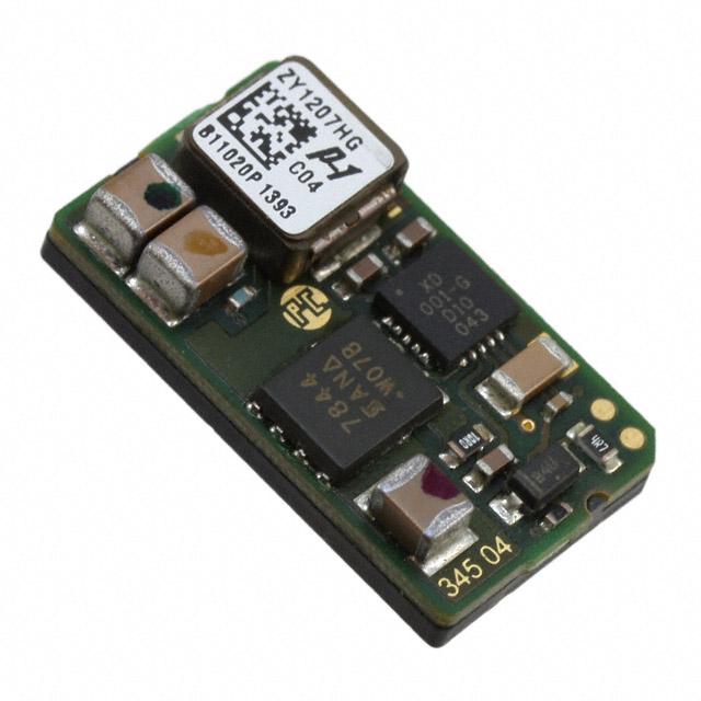
ZY1207 7A No-Bus POL Data Sheet
3V to 14V Input • 0.5V to 5.5V Output
Member of the
Applications
• Low voltage, high density systems with
Intermediate Bus Architectures (IBA)
• Point-of-load regulators for high performance DSP,
FPGA, ASIC, and microprocessor applications
• Desktops, servers, and portable computing
• Broadband, networking, optical, and
communications systems
• Active memory bus terminators
Benefits
• Integrates digital power conversion with intelligent
power management
• Eliminates the need for external power
management components and communication bus
• Completely programmable via pin strapping and
external R and C
• One part that covers all applications
• Reduces board space, system cost and
complexity, and time to market
Family
Features
• RoHS lead free and lead-solder-exempt products are
available
• Wide input voltage range: 3V–14V
• High continuous output current: 7A
• Wide programmable output voltage range: 0.5V–5.5V
• Active digital current share
• Output voltage margining
• Overcurrent and overtemperature protections
• Overvoltage and undervoltage protections, and Power
Good signal tracking the output voltage setpoint
• Programmable power-up delay
• Tracking during turn-on and turn-off with guaranteed
slew rates
• Sequenced and cascaded modes of operation
• Single-wire line for frequency synchronization
between multiple POLs
• Programmable interleave
• Programmable feedback loop compensation
• Enable control with programmable polarity
• Flexible fault management and propagation
• Start-up into the load pre-biased up to 100%
• Full rated current sink
• Real time current and temperature measurements,
monitoring, and reporting
• Small footprint SMT package: 12.5x22mm
• Low profile of 6.5mm
• Compatible with conventional pick-and-place
equipment
• Wide industrial operating temperature range
• UL 60950-1/CSA 22.2 No. 60950-1-07 Second
Edition, IEC 60950-1: 2005, and EN 60950-1:2006
Description
Power-One’s point-of-load converters are recommended for use with regulated bus converters in an Intermediate
Bus Architecture (IBA). The ZY1207 is an intelligent, fully programmable step-down point-of-load DC-DC module
integrating digital power conversion and intelligent power management. The ZY1207 completely eliminates the
need for external components for sequencing, tracking, protection, monitoring, and reporting. Performance
parameters of the ZY1207 are programmable by pin strapping and external resistor and capacitor and can be
changed by a user at any time during product development and service without a need for a communication bus.
ZD-00697 Rev. 2.1, 11-Oct-2011
www.power-one.com
Page 1 of 18
�ZY1207 7A No-Bus POL Data Sheet
3V to 14V Input • 0.5V to 5.5V Output
Reference Documents
TM
No-Bus POL Converters. Z-1000 Series Application Note
®
Z-One POL Converters. Eutectic Solder Process Application Note
®
Z-One POL Converters. Lead-Free Process Application Note
1.
Ordering Information
ZY
Product
family:
Z-One
Module
12
Series:
No-Bus
POL
Converter
07
Output
Current:
7A
x
Output voltage setpoint
accuracy:
No suffix – 1.5% or 35mV,
whichever is greater.
1
H – 1.5% or 20mV,
whichever is greater
y
RoHS compliance:
No suffix - RoHS
compliant with Pb
2
solder exemption
G - RoHS compliant
for all six substances
–
Dash
zz
3
Packaging Option :
T1 – 500pcs T&R
T2 – 100pcs T&R
T3 – 50pcs T&R
Q1 – 1pc sample for
evaluation only
K1 – 1pc mounted on
4
the evaluation board
______________________________________
1
Contact factory for availability.
The solder exemption refers to all the restricted materials except lead in solder. These materials are Cadmium (Cd), Hexavalent chromium
(Cr6+), Mercury (Hg), Polybrominated biphenyls (PBB), Polybrominated diphenylethers (PBDE), and Lead (Pb) used anywhere except in
solder.
3
Packaging option is used only for ordering and not included in the part number printed on the POL converter label.
4
The evaluation board is available in only one configuration: ZY1207-K1.
2
Example: ZY1207HG-T2: A 100-peices reel of RoHS compliant POL converters with the output voltage setpoint
of 1.5% or 20mV, whichever is greater. Each POL converter is labeled ZY1207HG.
2.
Absolute Maximum Ratings
Stresses in excess of the absolute maximum ratings may cause performance degradation, adversely affect longterm reliability, and cause permanent damage to the POL converter.
3.
Parameter
Conditions/Description
Min
Max
Units
Operating Temperature
Controller Case Temperature
-40
105
°C
Input Voltage
250ms Transient
15
VDC
Output Current
(See Output Current Derating Curves)
7
ADC
-7
Environmental and Mechanical Specifications
Parameter
Conditions/Description
Min
Nom
Max
Units
Ambient Temperature Range
-40
85
°C
Storage Temperature (Ts)
-55
125
°C
8
grams
Weight
MTBF
Calculated Per Telcordia Technologies SR-332
Peak Reflow Temperature
ZY1207
ZY1207G
Lead Plating
ZY1207 and ZY1207G
Moisture Sensitivity Level
ZY1207
ZY1207G
ZD-00697 Rev. 2.1, 11-Oct-2011
www.power-one.com
6.24
MHrs
220
°C
245
260
°C
100% Matte Tin or
1.5µm Ag over 1.5µm Ni
2
3
Page 2 of 18
�ZY1207 7A No-Bus POL Data Sheet
3V to 14V Input • 0.5V to 5.5V Output
4.
Electrical Specifications
Specifications apply at the input voltage from 3V to 14V, output load from 0 to 7A, ambient temperature from -40°C
to 85°C, output capacitance consisting of 110µF ceramic and 220µF tantalum, and default performance
parameters settings unless otherwise noted.
4.1
4.2
Input Specifications
Parameter
Conditions/Description
Min
Input voltage (VIN)
At VIN2.5V
75
100
30
15
25
25
40
mV
mV
µs
mV
mV
mV
mV
Temperature Coefficient
VIN=12V, IOUT=0.5*IOUT MAX
50
ppm/°C
Switching Frequency
450
500
550
1
kHz
At the negative output current (bus terminator mode) efficiency of the ZY1207 degrades resulting in increased internal power dissipation.
Therefore maximum allowable negative current under specific conditions is 20% lower than the current determined from the derating curves
shown in paragraph 5.5.
2
ZY1207 is a step-down converter, thus the output voltage is always lower than the input voltage as show in Figure 1.
3
Digital PWM has an inherent quantization uncertainty of ±6.25mV that is not included in the specified static regulation parameters.
ZD-00697 Rev. 2.1, 11-Oct-2011
www.power-one.com
Page 3 of 18
�ZY1207 7A No-Bus POL Data Sheet
3V to 14V Input • 0.5V to 5.5V Output
VOUT [V]
5.5
5.0
4.5
4.0
3.5
3.0
2.5
2.0
1.5
1.0
Min Load 0.2A
0.5
3.0
2.0
3.3
4.0
6.25
5.5
6.0
VIN [V]
8.0
10.0
12.0
14.0
Figure 1. Output Voltage as a Function of Input Voltage and Output Current
4.3
Protection Specifications
Parameter
Conditions/Description
Min
Nom
Max
Units
Output Overcurrent Protection
Type
Non-Latching, 130ms period
Threshold
140
Threshold Accuracy
%IOUT
-25
25
%IOCP.SET
Output Overvoltage Protection
Type
Latching
Threshold
Follows the output voltage setpoint
Threshold Accuracy
Measured at VO.SET=2.5V
Delay
From instant when threshold is exceeded until
the turn-off command is generated
130
-2
1
%VO.SET
2
%VOVP.SET
μs
6
Output Undervoltage Protection
Type
Threshold
Non-Latching, 130ms period
Follows the output voltage setpoint
Threshold Accuracy
Measured at VO.SET=2.5V
Delay
From instant when threshold is exceeded until
the turn-off command is generated
ZD-00697 Rev. 2.1, 11-Oct-2011
www.power-one.com
75
-2
%VO.SET
2
%VUVP.SET
μs
6
Page 4 of 18
�ZY1207 7A No-Bus POL Data Sheet
3V to 14V Input • 0.5V to 5.5V Output
Overtemperature Protection
Type
Non-Latching, 130ms period
Turn Off Threshold
Temperature is increasing
120
°C
Turn On Threshold
Temperature is decreasing after module was
shut down by OTP
110
°C
Threshold Accuracy
Delay
-5
From instant when threshold is exceeded until
the turn-off command is generated
°C
5
μs
6
Power Good Signal (PGOOD pin)
VOUT is inside the PG window and stable
VOUT is outside of the PG window or ramping
up/down
High
Follows the output voltage setpoint
90
%VO.SET
Upper Threshold
Follows the output voltage setpoint
110
%VO.SET
Delay
From instant when threshold is exceeded until
status of PG signal changes
6
μs
Threshold Accuracy
Measured at VO.SET=2.5V
Logic
Lower Threshold
N/A
Low
-2
2
%VO.SET
___________________
1
Minimum OVP threshold is 1.0V
4.4
Feature Specifications
Parameter
Conditions/Description
Min
Nom
Max
Units
Current Share (CS pin)
Type
Active, Single Line
Maximum Number of Modules
Connected in Parallel
IOUT MIN=0
Current Share Accuracy
IOUT MIN≥20%*IOUT NOM
Interleave (Phase Lag)
Programmable via INTL2…INTL4 pins in
45° steps
4
±20
%IOUT
315
degree
210
ms
Interleave (IM and INTL2…INTL4 pins)
0
Sequencing (DELAY pin)
Power-Up Delay
Programmable by capacitor connected to
DELAY pin
Default: CDELAY=0
0
ms
Tracking
Rising Slew Rate
Proportional to SYNC frequency
0.1
V/ms
Falling Slew Rate
Proportional to SYNC frequency
-0.5
V/ms
ZD-00697 Rev. 2.1, 11-Oct-2011
www.power-one.com
Page 5 of 18
�ZY1207 7A No-Bus POL Data Sheet
3V to 14V Input • 0.5V to 5.5V Output
Enable (EN and ENP pins)
ENP pin is pulled low
EN Pin Polarity
ENP pin is open
Negative (enables the output when EN pin is
pulled low)
Positive (enables the output when EN pin is
open or pulled high)
EN High Threshold
2.3
VDC
EN Low Threshold
Open Circuit Voltage
Turn-On Delay
Turn-Off Delay
1.0
EN and ENP
From EN pin changing state to VOUT
starting to ramp up
From EN pin changing state to VOUT
reaching 0V
VDC
3.3
VDC
0
ms
11
ms
Feedback Loop Compensation (CCA0…CCA2 pins)
CCA=7 (default)
CCA=6
CCA=5
CCA=3 or CCA=4
CCA=2
CCA=1
CCA=0
Recommended VIN range
Recommended COUT/ESR range,
combination of ceramic+ tantalum
Recommended VIN range
Recommended COUT range, tantalum
Recommended ESR range, tantalum
Recommended VIN range
Recommended COUT/ESR range, ceramic
Recommended VIN range
Recommended COUT/ESR range,
combination of ceramic + tantalum
Recommended VIN range
Recommended COUT/ESR range, tantalum
Recommended VIN range
Recommended COUT/ESR range, ceramic
Recommended VIN range
Recommended COUT/ESR range,
combination of ceramic+ tantalum
8
50/5 +
220/40
8
440
40
8
100/5
3
50/5 +
220/40
3
100/25
3
100/5
6
50/5 +
220/40
12
100/5 +
470/40
12
880
25
12
220/5
5
100/5 +
470/40
5
440/20
5
220/5
100/5 +
470/40
14
400/5 +
2000/20
14
10,000
10
14
400/5
5.5
200/5 +
880/40
5.5
1,000/10
5.5
400/5
11
200/5 +
880/40
VDC
µF/mΩ
µF/mΩ
VDC
µF
mΩ
VDC
µF/mΩ
VDC
µF/mΩ
µF/mΩ
VDC
µF/mΩ
VDC
µF/mΩ
VDC
µF/mΩ
µF/mΩ
+20
%IOUT
Output Current Monitoring (CS pin)
Output Current Monitoring
Accuracy
Conversion Ratio
20%*IOUT NOM < IOUT < IOUT NOM
VIN=12V
Duty Cycle of the negative pulse
corresponding to 100% of nominal current
-20
70
%
Temperature Monitoring (TEMP pin)
Temperature Monitoring
Accuracy
Junction temperature of POL controller
Conversion Ratio
Junction temperature from -40°C to 140°C
Monitoring Voltage Range
Corresponds to -40°C to 140°C junction
temperature range
Output Impedance
TEMP pin
-5
+5
10
0.2
°C
mV/°C
2
6.4
VDC
kΩ
Remote Voltage Sense (+VS pin)
Voltage Drop Compensation
ZD-00697 Rev. 2.1, 11-Oct-2011
Between +VS and VOUT
www.power-one.com
300
Page 6 of 18
mV
�ZY1207 7A No-Bus POL Data Sheet
3V to 14V Input • 0.5V to 5.5V Output
4.5
Signal Specifications
Parameter
Conditions/Description
Min
Nom
Max
Units
VDD
Internal supply voltage
3.15
3.3
3.45
V
0.3 x VDD
V
VDD + 0.5
V
0.45 x
VDD
V
SYNC Line
ViL_s
LOW level input voltage
-0.5
ViH_s
HIGH level input voltage
Vhyst_s
Hysteresis of input Schmitt trigger
IoL_s
LOW level sink current V(SYNC)=0.5V
14
60
mA
Ipu_s
Pull-up current source V(SYNC)=0V
300
1000
μA
Tr_s
Maximum allowed rise time 10/90%VDD
300
ns
Cnode_s
Added node capacitance
10
pF
Freq_s
Clock frequency of external SYNC line
0.75 x
VDD
0.25 x
VDD
5
475
525
Tsynq
Sync pulse duration
22
28
T0
Data=0 pulse duration
72
78
kHz
% of clock
cycle
% of clock
cycle
Inputs: INTL2…INTL4, CCA0…CCA2, EN, ENP, IM
Iup_x
Pull-up current source V(X)=0
25
110
μA
ViL_x
LOW level input voltage
-0.5
0.3 x VDD
V
ViH_x
HIGH level input voltage
0.7 x VDD
VDD+0.5
V
Vhyst_x
Hysteresis of input Schmitt trigger
0.1 x VDD
0.3 x VDD
V
RdnL_x
External pull down resistance
pin forced low
10
kOhm
Power Good and OK Inputs/Outputs
Iup_PG
Pull-up current source V(PG)=0
25
110
μA
Iup_OK
Pull-up current source V(OK)=0
175
725
μA
ViL_x
LOW level input voltage
-0.5
0.3 x VDD
V
ViH_x
HIGH level input voltage
0.7 x VDD
VDD+0.5
V
Vhyst_x
Hysteresis of input Schmitt trigger
0.1 x VDD
0.3 x VDD
V
IoL_x
LOW level sink current at 0.5V
4
20
mA
0.84
3.10
mA
-0.5
0.3 x VDD
V
VDD+0.5
V
0.45 x
VDD
V
60
mA
100
ns
Current Share/Sense Bus
Iup_CS
Pull-up current source at V(CS)=0V
ViL_CS
LOW level input voltage
ViH_CS
HIGH level input voltage
Vhyst_CS
Hysteresis of input Schmitt trigger
IoL_CS
LOW level sink current V(CS)=0.5V
Tr_CS
Maximum allowed rise time 10/90% VDD
ZD-00697 Rev. 2.1, 11-Oct-2011
www.power-one.com
0.75 x
VDD
0.25 x
VDD
14
Page 7 of 18
�ZY1207 7A No-Bus POL Data Sheet
3V to 14V Input • 0.5V to 5.5V Output
5.
Typical Performance Characteristics
5.1
94
Efficiency Curves
92
95
90
90
Efficiency, %
88
Efficiency, %
85
80
75
86
84
82
80
70
78
65
Vo=1.2V
Vo=2.5V
Vo=3.3V
Vo=5.0V
76
74
60
Vo=0.5V
Vo=1.2V
0
Vo=2.5V
1
2
55
3
4
5
6
7
Output Current, A
0
1
2
3
4
5
6
7
Output Current, A
Figure 4. Efficiency vs. Load. Vin=9.6V
Figure 2. Efficiency vs. Load. Vin=3.3V
92
90
95
88
86
Efficiency, %
90
Efficiency, %
85
80
75
84
82
80
78
76
74
70
72
65
Vo=0.5V
Vo=2.5V
60
Vo=1.2V
Vo=2.5V
Vo=3.3V
Vo=5.0V
70
Vo=1.2V
Vo=3.3V
0
1
2
3
4
5
Output Current, A
0
1
2
3
4
5
6
7
Output Current, A
Figure 5. Efficiency vs. Load. Vin=12V
Figure 3. Efficiency vs. Load. Vin=5V
ZD-00697 Rev. 2.1, 11-Oct-2011
www.power-one.com
Page 8 of 18
6
7
�ZY1207 7A No-Bus POL Data Sheet
3V to 14V Input • 0.5V to 5.5V Output
95
5.2
Turn-On Characteristics
90
Efficiency, %
85
80
75
70
65
Vin=5V
Vin=3.3V
Vin=9.6V
Vin=12V
60
55
0.5
1.5
2.5
3.5
4.5
5.5
Output Voltage, V
Figure 6. Efficiency vs. Output Voltage, Iout=7A
Figure 8. Tracking Turn-On.
Vin=12V, Ch1 – V1, Ch2 – V2, Ch3 – V3
5.3
90
Turn-Off Characteristics
85
Efficiency, %
80
75
70
65
60
55
Vo=0.5V
Vo=1.2V
Vo=2.5V
50
3
4
5
6
7
8
9
10 11 12
13 14
Input Voltage, V
Figure 9. Tracking Turn-Off
Vin=12V, Ch1 – V1, Ch2 – V2, Ch3 – V3
Figure 7. Efficiency vs. Input Voltage. Iout=7A
5.4
Transient Response
The pictures in Figure 10 - Figure 15 show the
deviation of the output voltage in response to the 5075-50% step load at 1.0A/μs. In all tests the POL
converters had 5x22μF ceramic capacitors and a
220μF tantalum capacitor connected across the
output pins. The speed of the transient response
was optimized by selecting appropriate CCA
settings.
ZD-00697 Rev. 2.1, 11-Oct-2011
www.power-one.com
Page 9 of 18
�ZY1207 7A No-Bus POL Data Sheet
3V to 14V Input • 0.5V to 5.5V Output
Figure 10. Vin=12V, Vout=1V. CCA=00
Figure 13. Vin=5V, Vout=1V. CCA=03
Figure 11. Vin=12V, Vout=2.5V. CCA=00
Figure 14. Vin=5V, Vout=2.5V. CCA=03
Figure 12. Vin=12V, Vout=5V, CCA=00
Figure 15. Vin=3.3V, Vout=1V. CCA=03
ZD-00697 Rev. 2.1, 11-Oct-2011
www.power-one.com
Page 10 of 18
�ZY1207 7A No-Bus POL Data Sheet
3V to 14V Input • 0.5V to 5.5V Output
5.5
Thermal Derating Curves
7
Output Current, A
6.5
6
5.5
5
4.5
4
3.5
0LFM
3
45
100LFM
55
200LFM
400LFM
65
600LFM
75
85
Ambient Temperature, Degree C
Figure 16. Thermal Derating Curves. Vin=12V, Vout=5.0V
7
Output Current, A
6.5
6
5.5
5
4.5
4
3.5
0LFM
3
45
100LFM
55
200LFM
400LFM
65
600LFM
75
85
Ambient Temperature, Degree C
Figure 17. Thermal Derating Curves. Vin=14V, Vout=5.0V
ZD-00697 Rev. 2.1, 11-Oct-2011
www.power-one.com
Page 11 of 18
�ZY1207 7A No-Bus POL Data Sheet
3V to 14V Input • 0.5V to 5.5V Output
6.
Typical Application
IBV
ENABLE
CS
SYNC
CS
OK
SYNC
OK
TRIM
PGOOD
TRIM
PGOOD
VREF
TEMP
VREF
TEMP
VLDO
VIN
VIN
VIN
VIN
VIN
EN
ENP
ENP
CCA2
CCA1
CCA2
POL2
22uF 4.7uF 4.7uF
CCA1
POL4
22uF 4.7uF 4.7uF
CCA0
CCA0
+VS
VOUT
VOUT
VOUT
VOUT
VOUT
INTL4
INTL3
INTL2
INTL3
INTL2
47uF
DELAY
SYNC
DELAY
CS
SYNC
OK
TRIM
PGOOD
TRIM
PGOOD
VREF
TEMP
VREF
TEMP
VLDO
VIN
VIN
VIN
VIN
VIN
ENP
ENP
CCA2
POL1
22uF 4.7uF 4.7uF
CCA1
INTL3
INTL2
+VS
VOUT
VOUT
VOUT
VOUT
VOUT
INTL4
INTL3
220uF
IM
DELAY
POL3
22uF 4.7uF 4.7uF
CCA0
CCA0
INTL4
VLDO
VIN
VIN
VIN
VIN
VIN
EN
CCA2
CCA1
47uF
47uF
PGND
PGND
PGND
PGND
PGND
PGND
PGND
IM
OK
EN
Vo2
220uF
47uF
PGND
PGND
PGND
PGND
PGND
PGND
PGND
IM
+VS
VOUT
VOUT
VOUT
VOUT
VOUT
INTL4
220uF
CS
VLDO
VIN
VIN
VIN
VIN
VIN
EN
47uF
47uF
Vo1
PGND
PGND
PGND
PGND
PGND
PGND
PGND
INTL2
+VS
VOUT
VOUT
VOUT
VOUT
VOUT
Vo3
220uF
IM
DELAY
47uF
47uF
PGND
PGND
PGND
PGND
PGND
PGND
PGND
Figure 18. Complete Schematic of Application with Three Independent Outputs. Intermediate Bus Voltage is from 8V to 14V.
In this application four POL converters are configured to deliver three independent output voltages. POL1 and
POL2 are connected in parallel for increased output current. Output voltages are programmed with the resistors
connected between TRIM and VREF pins of individual converters.
POL1 is configured as a master (IM and INTL0…INTL4 pins are grounded) and all other POL converters are
synchronized to the switching frequency of POL1. Interleave is programmed with pins INTL0…INTL4 to ensure
the lowest input and output noise. POL2 has 180° phase shift, POL 3 and POL4 have phase shifts of 270° and
90° respectively.
All converters are controlled by the common ENABLE signal. Turn-on and turn-off processes of the system are
illustrated by pictures in Figure 8 and Figure 9.
ZD-00697 Rev. 2.1, 11-Oct-2011
www.power-one.com
Page 12 of 18
�ZY1207 7A No-Bus POL Data Sheet
3V to 14V Input • 0.5V to 5.5V Output
7.
Pin Assignments and Description
Pin
Name
Pin
No.
Pin
Type
Buffer
Type
Pin Description
Notes
VLDO
1
P
Low Voltage Dropout
Connect to an external voltage source higher
than 4.75V, if VIN


 工商网监
湘ICP备2023018690号
工商网监
湘ICP备2023018690号
