VersaClock® Low-power Clock Generator
5P49EE802
DATASHEET
Description
Features
The 5P49EE802 is a programmable clock generator intended
for low power, battery operated consumer applications. There
are four internal PLLs, each individually programmable,
allowing for up to eight different output frequencies. The
frequencies are generated from a single reference clock. The
reference clock can come from either a TCXO or fundamental
mode crystal. An additional 32kHz crystal oscillator is
available to provide a real time clock or non-critical
performance MHz processor clock.
•
•
•
•
•
•
•
The 5P49EE802 can be programmed through the use of the
I2C interfaces. The programming interface enables the device
to be programmed when it is in normal operation or what is
commonly known as in system programmable. An internal
EEPROM allows the user to save and restore the
configuration of the device without having to reprogram it on
power-up.
•
•
Each of the four PLLs has an 8-bit reference divider and a
11-bit feedback divider. This allows the user to generate four
unique non-integer-related frequencies. The PLL loop
bandwidth is programmable to allow the user to tailor the PLL
response to the application. For instance, the user can tune
the PLL parameters to minimize jitter generation or to
maximize jitter attenuation. Spread spectrum generation is
supported on one of the PLLs.
•
•
•
•
•
•
Spread spectrum generation is supported on one of the PLLs.
The device is specifically designed to work with display
applications to ensure that the spread profile remains
consistent for each HSYNC in order to reduce ROW noise. It
also may operate in standard spread spectrum mode.
•
•
•
There are total seven 8-bit output dividers. Outputs are
LVCMOS. The outputs are connected to the PLLs via the
switch matrix. The switch matrix allows the user to route the
PLL outputs to any output bank. This feature can be used to
simplify and optimize the board layout. In addition, each
output's slew rate and enable/disable function can be
programmed.
Four internal PLLs
Internal non-volatile EEPROM
Internal I2C EEPROM master interface
FAST (400kHz) mode I2C serial interfaces
Input Frequencies
– TCXO: 10 MHz to 40 MHz
– Crystal: 8 MHz to 30 MHz
– RTC Crystal: 32.768 kHz
Output Frequency Ranges: kHz to 120 MHz
Each PLL has an 8-bit reference divider and a 11-bit
feedback-divider
8-bit output-divider blocks
One of the PLLs support Spread Spectrum generation
capable of configuration to pixel rate, with adjustable
modulation rate and amplitude to support video clock with
no visible artifacts
I/O Standards:
– Outputs - 1.8V/2.5V/3.3 V LVTTL/ LVCMOS
– 3 independent adjustable VDDO groups
Programmable Slew Rate Control
Programmable Loop Bandwidth Settings
Programmable output inversion to reduce bimodal jitter
Individual output enable/disable
Power-down/Sleep mode
– 10A max in power down mode
– 32kHz clock output active sleep mode
– 100A max in sleep mode
1.8V VDD Core Voltage
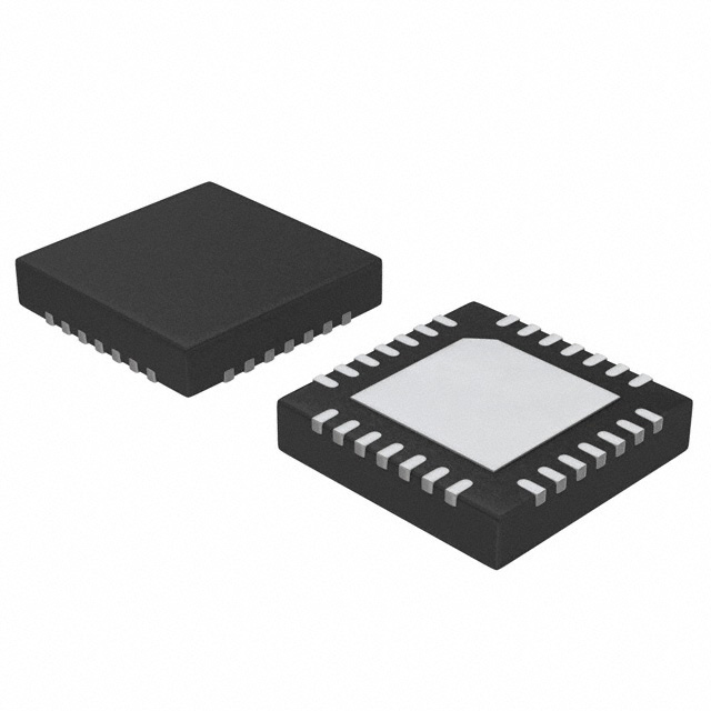
Available in 28 pin 4x4mm QFN packages
-40 to +85°C Industrial Temp operation
Target Applications
•
•
•
•
•
•
Smart Mobile Handset
Personal Navigation Device (PND)
Camcorder
DSC
Portable Game Console
Personal Media Player
5P49EE802 REVISION P 04/01/16
1
©2016 Integrated Device Technology, Inc.
�5P49EE802 DATASHEET
Functional Block Diagram
VDD
VDDO1
VDDO2
VDDO3
S
R
C
0
/DIV0
OUT0
S
R
C
1
/DIV1
OUT1
PLLB(SS)
S
R
C
2
/DIV2
OUT2
PLLC
S
R
C
3
/DIV3
OUT3
/DIV4
OUT4
S
R
C
5
/DIV5
OUT5
S
R
C
6
/DIV6
XIN/REF
PLLA
XOUT
REFSEL0
REFSEL1
SDA
SCL
Control
Logic
REFSEL2
SEL[1:0]
S
R
C
4
REFSEL3
PLLD
32kXIN
32kXOUT
OUT6A
OUT6B
GND
VERSACLOCK® LOW-POWER CLOCK GENERATOR
2
REVISION P 04/01/16
�5P49EE802 DATASHEET
Pin Assignment
SDA
OUT6A
VDD
VDD
GND
XIN/REF
XOUT
OUT5
1
28 27 26 25 24 23 22
21
OUT4
2
20
SCLK
OUT3
3
19
VDDO3
SEL0
4
18
OUT0
VDD
OUT6B
VDDO1
5
17
X1_32
6
16
VDD
X2_32
7
15
OUT1
8
9 10 11 12 13 14
SEL1
OUT2
VDD
VDDO2
GND
GND
VDDx
28 pin VFQFPN
(Top View)
Pin Descriptions
Pin Name
Pin #
I/O
Pin Type
Pin Description
OUT5
1
O
Adjustable
Configurable clock output 5. Single-ended output voltage levels
are register controlled by either VDDO1, VDDO2 or VDDO3.
OUT4
2
O
Adjustable
Configurable clock output 4. Single-ended output voltage levels
are register controlled by either VDDO1, VDDO2 or VDDO3.
OUT3
3
O
Adjustable
Configurable clock output 3. Single-ended output voltage levels
are register controlled by either VDDO1, VDDO2 or VDDO3.
SEL0*
4
I
LVTTL
Configuration select pin. Weak internal pull down resistor.
VDDO1
5
Power
Device power supply. Connect to 1.8 to 3.3V. Using register
settings, select output voltage levels for OUT0-OUT6. VDDO1
must be greater than or equal to both VDDO2 and VDDO3.
X132k
6
I
LVTTL
32kHz CRYSTAL_IN -- Reference crystal input
X232k
7
I
LVTTL
32kHz CRYSTAL_OUT -- Reference crystal feedback.
VDDx
8
Power
Crystal oscillator power supply. Connect to 1.8V. Use filtered
analog power supply if available.
GND
9
Power
Connect to Ground.
GND
10
Power
Connect to Ground.
VDD
11
Power
Device power supply. Connect to 1.8V.
VDDO2
12
Power
Device power supply. Connect to 1.8 to 3.3V. Using register
settings, select output voltage levels for OUT0-OUT5.
OUT2
13
O
Adjustable
SEL1*
14
I
LVTTL
OUT1
15
O
Adjustable
REVISION P 04/01/16
Configurable clock output 2. Single-ended output voltage levels
are register controlled by either VDDO1, VDDO2 or VDDO3.
Configuration select pin. Weak internal pull down resistor.
Configurable clock output 1. Single-ended output voltage levels
are register controlled by either VDDO1, VDDO2 or VDDO3.
3
�5P49EE802 DATASHEET
Pin Name
Pin #
I/O
VDD
16
Power
Device power supply. Connect to 1.8V.
VDD
17
Power
Device power supply. Connect to 1.8V.
OUT0
18
VDDO3
19
SCLK
20
OUT6B
O
Pin Type
Adjustable
Pin Description
Configurable clock output 0. Single-ended output voltage levels
are register controlled by either VDDO1, VDDO2 or VDDO3.
Power
Device power supply. Connect to 1.8 to 3.3V. Using register
settings, select output voltage levels for OUT0-OUT5.
I
LVTTL
I2C clock. Logic levels set by VDDO1. 5V tolerant.
21
O
Adjustable
Configurable clock output 6B. Output voltage levels are
controlled by VDDO1.
OUT6A
22
O
Adjustable
Configurable clock output 6A. Output voltage levels are
controlled by VDDO1.
SDA
23
I/O
LVTTL
Bidirectional I2C data. Logic levels set by VDDO1. 5V tolerant.
VDD
24
Power
Device power supply. Connect to 1.8V.
VDD
25
Power
Device power supply. Connect to 1.8V.
GND
26
Power
Connect to Ground.
XIN/ REF
27
I
LVTTL
MHz CRYSTAL_IN -- Reference crystal input or external
reference clock input. Maximum clock input voltage is 1.8V.
XOUT
28
O
LVTTL
MHz CRYSTAL_OUT -- Reference crystal feedback. Float pin if
using reference input clock.
Note *: SEL pins should be controlled by 1.8V LVTTL logic; 3.3V tolerant.
Note 1: Outputs are user programmable to drive single-ended 1.8V/2.5V/3.3V LVTTL as indicated above. Always
completely power up VDD and VDDx prior to applying VDDO power.
Note 2: Default factory configuration OUT4=buffered reference output & OUT2=32.768KHz. All other outputs are off.
Note 3: Do not power up with SEL[1:0] = 00 (in Power down/Sleep mode).
Ideal Power Up Sequence
Ideal Power Down Sequence
1) VDDO must drop first, followed by VDD and VDDx
2) VDD and VDDx must come down within 1ms after VDDO1 comes down
3) VDDO2/3 must be equal to, or lower than, VDDO1
4) VDD and VDDx have approx. the same ramp rate
5) VDDO1 and VDDO2/3 have approx. same ramp rate
1) VDD and VDDx must come up first, followed by VDDO
2) VDDO1 must come up within 1ms after VDD and VDDX come up
3) VDDO2/3 must be equal to, or lower than, VDDO1
4) VDD and VDDx have approx. the same ramp rate
5) VDDO1 and VDDO2/3 have approx. same ramp rate
V
V
VDDO1
VDDO1
VDDO2, VDDO3
VDD, VDDx
VDDO2, VDDO3
VDD, VDDx
1 ms
1 ms
VERSACLOCK® LOW-POWER CLOCK GENERATOR
t
t
4
REVISION P 04/01/16
�5P49EE802 DATASHEET
PLL Features and Descriptions
VCO
D
M
XDIV
PLL Block Diagram
Ref-Divider
(D) Values
Feedback
Feedback (M)
Pre-Divider
Values
(XDIV) Values
Programmable
Loop Bandwidth
Spread Spectrum
Generation Capability
PLLA
1 - 255
1 or 4
6 - 2047
Yes
No
PLLB
1 - 255
4
6 - 2047
Yes
Yes
PLLC
1 - 255
1 or 8 bit divide
6 - 2047
Yes
No
PLLD
1 - 255
1 or 4
6 - 2047
Yes
No
Crystal Input (XIN/REF)
Reference Pre-Divider, Reference Divider,
Feedback-Divider and Post-Divider
The crystal oscillators should be fundamental mode quartz
crystals; overtone crystals are not suitable. Crystal frequency
should be specified for parallel resonance with 50 maximum
equivalent series resonance. 0
Each PLL incorporates an 8-bit reference-scaler and a 11-bit
feedback divider which allows the user to generate four
unique non-integer-related frequencies. PLLA and PLLD each
have a feedback pre-divider that provides additional
multiplication for kHz reference clock applications. Each
output divider supports 8-bit post-divider. The following
equation governs how the output frequency is calculated.
ONXTALB=0 bit needs to be set for XIN/REF.
Crystal Load Capacitors
The device crystal connections should include pads for small
capacitors from X1 to ground and from X2 to ground. These
capacitors are used to adjust the stray capacitance of the
board to match the nominally required crystal load
capacitance. Because load capacitance can only be
increased in this trimming process, it is important to keep stray
capacitance to a minimum by using very short PCB traces
(and no vias) between the crystal and device. Crystal
capacitors must be connected from each of the pins X1 and
X2 to ground.
XDIV*M
FOUT = FIN * (
)
D (Eq. 2)
ODIV
Where FIN is the reference frequency, XDIV is the feedback
pre-divider value, M is the feedback-divider value, D is the
reference divider value, ODIV is the total post-divider value,
and FOUT is the resulting output frequency. Programming any
of the dividers may cause glitches on the outputs.
The crystal capacitors are internal to the device and have an
effective value of 4pF.
REVISION P 04/01/16
5
VERSACLOCK® LOW-POWER CLOCK GENERATOR
�5P49EE802 DATASHEET
Spread Spectrum Generation (PLLB)
FMID = FVCO/8
PLLB has spread spectrum generation capability, which users
have the option of turning on and off. Spread spectrum profile,
frequency, and spread are fully programmable (within limits).
The programmable spread spectrum generation parameters
are NC[10:0], MOD[12:0], and NSS[10:0] bits. To enable
spread spectrum, set SSENB_B=0.
NC = 640 (integer number of spread periods/screen)
MOD = (25MHz * 640)/(2 * 54MHz) = 160
NSS = (640/2)+(640/8)*(27.27MHz-26.73MHz)/27MHz = 321.
FMOD = 27MHz/640 = 11.8kHz.
The spread spectrum circuitry was specifically developed to
accommodate video display applications. The spread
modulation frequency can be defined to exactly equal the
horizontal line frequency (HSYNC)
Non-Video Example
FREF = 25MHz, FOUT = 27 MHz, 31.25kHz modulation rate,
center spread of ±1%. Find the necessary spread spectrum
register settings.
NC[10:0]
These bits are used to determine the number of pulses per
spread spectrum cycle. For video applications, NC is the
number of pixels on the horizontal display row (or integer
multiple of displayed pixels in a row). By matching the spread
period to the screen, no tearing or “shimmer” will be apparent.
FMID = FVCO/ 8
FMOD = 31.25kHz = 50.625MHz/NC.
NC = 1620
NC must be an even number to insure that the upward spread
transition has the same number of steps as the downward
spread transition.
MOD = (25MHz * 1620)/(2 * 50.625MHz) = 400
NSS = (1620/2)+(1620/8)*(27.27MHz-26.73MHz)/27MHz =
814.
For non-video applications, this can also be seen as the
number of clock cycles for a complete spread spectrum
period.
MOD[12:0]
These bits relate the VCO frequency to the target average
spread output frequency (FMID).
FMID = (FVCO) / 8
FMAX = FMID + (SS% * FMID)
FMIN = FMID - (SS% * FMID)
MOD = (FREF* NC) / (2 * FMID)
NSS[10:0]
These bits control the amplitude of the spread modulation.
NSS = (NC / 2) + (NC / 8) * (FMAX - FMIN) / FMID
Modulation frequency:
FMOD = FMID / NC (Eq. 11)
Video Example
FREF = 27 MHz, FOUT = 27 MHz, 640 pixels per line, center
spread of ±1%. Using FVCO=432MHz, find the necessary
spread spectrum register settings.
VERSACLOCK® LOW-POWER CLOCK GENERATOR
6
REVISION P 04/01/16
�5P49EE802 DATASHEET
VSYNC, HSYNC, DOT_CLK – Modulation Rate Relationship
VSYNC
HSYNC
Integer multiple of HSYNC periods
DOT_CLK
Modulation
Rate
X/2
X/2
X
X
X = Number of cycles of DOT_CLK per HSYNC period.
X/2 = Number of cycles of DOT_CLK that the modulation edge rises/falls.
Loop Filter
The loop filter for each PLL can be programmed to optimize
the jitter performance. The low-pass frequency response of
the PLL is the mechanism that dictates the jitter transfer
characteristics. The loop bandwidth can be extracted from the
jitter transfer. A narrow loop bandwidth is good for jitter
attenuation while a wide loop bandwidth is best for low jitter
generation. The specific loop filter components that can be
programmed are the resistor via the RZ[4:0] bits, zero
capacitor via the CZ[2:0] bits, pole capacitor via the CP[1:0]
bits, and the charge pump current via the IP#[2:0] bits.
The following equations govern how the loop filter is set:
Zero capacitor (Cz) = 280pF
Pole capacitor (Cp) = 30pF
Charge pump (Ip) = IP#[2:0] uA
VCO gain (KVCO) = 350MHz/V * 2
REVISION P 04/01/16
7
VERSACLOCK® LOW-POWER CLOCK GENERATOR
�5P49EE802 DATASHEET
PLL Loop Bandwidth:
Charge pump gain (K) = Ip / 2
Solving for Rz, the best possible value Rz=30kOhms
(RZ[1:0]=10) gives
VCO gain (KVCO) = 350MHz/V * 2
= 1.4 (Ideal range for is 0.7 to 1.4)
M = Total multiplier value (See the PRE-SCALERS,
FEEDBACK-DIVIDERS, POST-DIVIDERS section for more
detail)
Solving back for the PLL loop bandwidth, Fc=149kHz.
c = (Rz * K* KVCO * Cz)/(M * (Cz + Cp))
m = (360 / 2) * [tan-1 (9.42x10⁵ s-1 / 1.19x10⁵s-1)
- tan-1(9.42x10⁵ s-1/ 1.23x10⁶ s-1)] = 45°
The phase margin must be checked for loop stability.
Fc = c / 2
The phase margin would be acceptable with a fairly stable
loop.
Note, the phase/frequency detector frequency (FPFD) is
typically seven times the PLL closed-loop bandwidth (Fc) but
too high of a ratio will reduce your phase margin thus
compromising loop stability.
To determine if the loop is stable, the phase margin (m)
would need to be calculated as follows.
Phase Margin:
z = 1 / (Rz * Cz)
p = (Cz + Cp)/(Rz * Cz * Cp)
m = (360 / 2) * [tan-1(c/ z) - tan-1(c/ p)]
To ensure stability in the loop, the phase margin is
recommended to be > 60° but too high will result in the lock
time being excessively long. Certain loop filter parameters
would need to be compromised to not only meet a required
loop bandwidth but to also maintain loop stability.
Damping Factor:
= Rz/2 *(KVCO * Ip * Cz)1/2/M
Example
Fc = 150KHz is the desired loop bandwidth. The total A*M
value is 160. The (damping factor) target should be 0.7,
meaning the loop is critically damped. Given Fc and A*M, an
optimal loop filter setting needs to be solved for that will meet
both the PLL loop bandwidth and maintain loop stability.
Choose a mid-range charge pump from register table
Icp= 11.9uA.
K* KVCO = 350MHz/V * 40uA = 12000A/Vs
c = 2* Fc = 9.42x10⁵ s-1
p = (Cz + Cp)/(Rz * Cz * Cp) = z (1 + Cz / Cp)
VERSACLOCK® LOW-POWER CLOCK GENERATOR
8
REVISION P 04/01/16
�5P49EE802 DATASHEET
SEL[1:0] Function
The 5P49EE802 can support up to three unique
configurations. Users may pre-program all configurations,
selected using SEL[1:0] pins. Alternatively, users may use I2C
interface to configure these registers on- the-fly.
Power Down/Sleep Mode is selected by the No_PD bit. No_PD=0
enables Power Down mode with no outputs. No_PD=1 enables
sleep mode with 32kHz output on OUT2.
Always power with SEL1=1 and/or SEL0=1.
.
SEL1
SEL0
Configuration Selections
0
0
Power Down/Sleep Mode
0
1
Select CONFIG0
1
0
Select CONFIG1
1
1
Select CONFIG2
Configuration OUTx IO Standard
Users can configure the individual output IO standard from a
single 3.3V power supply. Each output can support 1.8V/ 2.5V
or 3.3V LVCMOS. VDDO1 must have the highest voltage of
any pin on the device. VDDO2 and VDDO3 may have any
value between 1.8V and VDDO1.
Programming the Device
I2C may be used to program the 5P49EE802.
The frame formats are shown in the following illustration.
– Device (slave) address = 7'b1101010
I2C Programming
The 5P49EE802 is programmed through an I2C-Bus serial
interface, and is an I2C slave device. The read and write
transfer formats are supported. The first byte of data after a
write frame to the correct slave address is interpreted as the
register address; this address auto-increments after each byte
written or read.
Framing
First Byte Transmitted on I2C Bus
REVISION P 04/01/16
9
VERSACLOCK® LOW-POWER CLOCK GENERATOR
�5P49EE802 DATASHEET
External I2C Interface Condition
EEPROM Interface
is issued by the Master, during which time the 5P49EE802 will
not generate Acknowledge bits. The 5P49EE802 will
acknowledge the instructions after it has completed execution
of them. During that time, the I2C bus should be interpreted as
busy by all other users of the bus.
The 5P49EE802 can store its configuration in an internal
EEPROM. The contents of the device's internal programming
registers can be saved to the EEPROM by issuing a save
instruction (ProgSave) and can be loaded back to the internal
programming registers by issuing a restore instruction
(ProgRestore).
On power-up of the 5P49EE802, an automatic restore is
performed to load the EEPROM contents into the internal
programming registers. The 5P49EE802 will be ready to
accept a programming instruction once it acknowledges its
7-bit I2C address.
To initiate a save or restore using I2C, only two bytes are
transferred. The Device Address is issued with the read/write
bit set to “0”, followed by the appropriate command code. The
save or restore instruction executes after the STOP condition
Progwrite
Progwrite Command Frame
Writes can continue as long as a Stop condition is not sent and each byte will increment the register address.
VERSACLOCK® LOW-POWER CLOCK GENERATOR
10
REVISION P 04/01/16
�5P49EE802 DATASHEET
Progread
Note: If the expected read command is not from the next higher register to the previous read or write command, then
set a known “read” register address prior to a read operation by issuing the following command:
Prior to Progread Command Set Register Address
The user can ignore the STOP condition above and use a repeated START condition instead, straight after the slave
acknowledgement bit (i.e., followed by the Progread command):
S
Address
R/W
ACK
ID Byte
ACK
Data_1
ACK
Data_2
ACK
7-bits
1
1-bit
8-bits
1-bit
8-bits
1-bit
8-bits
1-bit
Data_last NACK
8-bits
P
1-bit
Progread Command Frame
Progsave
Note:
PROGWRITE is for writing to the 5P49EE802 registers.
PROGREAD is for reading the 5P49EE802 registers.
PROGSAVE is for saving all the contents of the 5P49EE802
registers to the EEPROM.
PROGRESTORE is for loading the entire EEPROM contents
to the 5P49EE802 registers.
Progrestore
During PROGRESTORE, outputs will be turned off to ensure
that no improper voltage levels are experienced before
initialization.
REVISION P 04/01/16
11
VERSACLOCK® LOW-POWER CLOCK GENERATOR
�5P49EE802 DATASHEET
I2C Bus DC Characteristics
Symbol
Parameter
VIH
Input HIGH Level
VIL
Input LOW Level
VHYS
IIN
VOL
Conditions
Min
Typ
0.7xVDDO1
Hysteresis of Inputs
Max
Unit
5.5
V
0.3xVDDO1
V
0.05xVDDO1
V
Input Leakage Current
VDD = 0V
±1.0
µA
Output LOW Voltage
IOL = 3 mA
0.4
V
I2C Bus AC Characteristics for Standard Mode
Symbol
FSCLK
tBUF
Parameter
Min
Serial Clock Frequency (SCL)
0
Typ
Max
Unit
100
kHz
Bus free time between STOP and START
4.7
µs
tSU:START
Setup Time, START
4.7
µs
tHD:START
Hold Time, START
4
µs
tSU:DATA
Setup Time, data input (SDA)
250
ns
tHD:DATA
Hold Time, data input (SDA)
1
0
µs
tOVD
Output data valid from clock
3.45
µs
CB
Capacitive Load for Each Bus Line
400
pF
tR
Rise Time, data and clock (SDA, SCLK)
1000
ns
tF
Fall Time, data and clock (SDA, SCLK)
300
ns
tHIGH
HIGH Time, clock (SCLK)
4
µs
tLOW
LOW Time, clock (SCLK)
4.7
µs
4
µs
tSU:STOP
Setup Time, STOP
1) No activity is allowed on I2C lines until VDD>1.62V.
2) A device must internally provide a hold time of at least 300 ns for the SDA signal (referred to the VIHMIN of the SCLK
signal) to bridge the undefined region of the falling edge of SCLK.
VERSACLOCK® LOW-POWER CLOCK GENERATOR
12
REVISION P 04/01/16
�5P49EE802 DATASHEET
I2C Bus AC Characteristics for Fast Mode
Symbol
FSCLK
tBUF
Parameter
Min
Serial Clock Frequency (SCL)
0
Typ
Max
Unit
400
kHz
Bus free time between STOP and START
1.3
µs
tSU:START
Setup Time, START
0.6
µs
tHD:START
Hold Time, START
0.6
µs
tSU:DATA
Setup Time, data input (SDA)
100
ns
tHD:DATA
Hold Time, data input (SDA)
1
0
µs
tOVD
Output data valid from clock
0.9
µs
CB
Capacitive Load for Each Bus Line
400
pF
tR
Rise Time, data and clock (SDA, SCL)
20 + 0.1xCB
300
ns
tF
Fall Time, data and clock (SDA, SCL)
20 + 0.1xCB
300
ns
tHIGH
HIGH Time, clock (SCL)
0.6
µs
tLOW
LOW Time, clock (SCL)
1.3
µs
Setup Time, STOP
0.6
µs
tSU:STOP
1) No activity is allowed on I2C lines until VDD>1.62V.
2) A device must internally provide a hold time of at least 300 ns for the SDA signal (referred to the VIHMIN of the SCL
signal) to bridge the undefined region of the falling edge of SCL.
REVISION P 04/01/16
13
VERSACLOCK® LOW-POWER CLOCK GENERATOR
�5P49EE802 DATASHEET
Absolute Maximum Ratings
Stresses above the ratings listed below can cause permanent damage to the 5P49EE802. These ratings, which are standard
values for IDT commercially rated parts, are stress ratings only. Functional operation of the device at these or any other
conditions above those indicated in the operational sections of the specifications is not implied. Exposure to absolute maximum
rating conditions for extended periods can affect product reliability. Electrical parameters are guaranteed only over the
recommended operating temperature range.
Symbol
Description
Max
Unit
Internal Power Supply Voltage
-0.5 to +4.6
V
VI
Input Voltage
-0.5 to +4.6
V
VO
Output Voltage (not to exceed 4.6 V)
-0.5 to VDD+0.5
V
TJ
Junction Temperature
150
°C
TSTG
Storage Temperature
-65 to +150
°C
VDD
Recommended Operation Conditions
Symbol
Parameter
VDD , VDDx
VDDOX
TA
Min
Typ
Max
Unit
Power supply voltage for core VDD
1.71
1.8
1.89
V
Power supply voltage for outputs VDDO1/2/3
1.71
1.8
1.89
V
2.375
2.5
2.625
V
3.135
3.3
3.465
V
+85
°C
Operating temperature, ambient
-40
CLOAD_OUT
Maximum load capacitance (3.3V LVTTL only)
15
pF
CLOAD_OUT
Maximum load capacitance (1.8V or 2.5V LVTTL only)
8
pF
MHz
FIN
tPU
External reference crystal
8
30
External reference clock CLKIN
1
40
0.05
5
Power up time for all VDDs to reach minimum specified
voltage (power ramps must be monotonic)
ms
Capacitance (TA = +25 °C, f = 1 MHz, VIN = 0V)
Symbol
CIN
Parameter
Min
Typ
Input Capacitance
Max
Unit
3
pF
Crystal Specifications
XTAL_FREQ
Crystal frequency
8
30
MHz
XTAL_MIN
Minimum crystal load capacitance
7
pF
XTAL_MAX
Maximum crystal load capacitance
20
pF
DC Electrical Characteristics for 3.3V LVTTL 1
Symbol
Parameter
Test Conditions
VOH
Output HIGH Voltage
IOH = 33mA
VOL
Output LOW Voltage
IOH = 33mA
Output Leakage Current
3-state outputs
IOZDD
VERSACLOCK® LOW-POWER CLOCK GENERATOR
Min
2.4
14
Typ
Max
Unit
VDDO
V
0.4
V
5
µA
REVISION P 04/01/16
�5P49EE802 DATASHEET
DC Electrical Characteristics for 2.5V LVTTL 1
Symbol
Parameter
Test Conditions
VOH
Output HIGH Voltage
IOH = 25mA
VOL
Output LOW Voltage
IOH = 25mA
Output Leakage Current
3-state outputs
IOZDD
Min
Typ
2.1
Max
Unit
VDDO
V
0.4
V
5
µA
Max
Unit
VDDO
V
0.6
V
DC Electrical Characteristics for 1.8V LVTTL 1
Symbol
Parameter
Test Conditions
VOH
Output HIGH Voltage
VOL
Output LOW Voltage
VIH
Input HIGH Voltage
SEL[1:0], 3.3V tolerant
VIL
Input LOW Voltage
SEL[1:0], 3.3V tolerant
Output Leakage Current
3-state outputs
IOZDD
Min
VDDO = 1.71V to 1.89V
Typ
1.23
1.35
V
0.45
V
5
µA
Power Supply Characteristics for LVTTL Outputs
Total Supply Current Vs VCO Frequency
Supply current Vs Output Frequency
14
12
10
8
6
4
2
0
Supply Current(mA)
Total Supply
Current(mA)
30
0
100
200
300
25
20
15
10
5
0
400
0
VCO Frequency(MHz)
20
40
60
80
1 PLL ON IDD (mA)
2 PLLs On IDD (mA)
Output Frequency(MHz)
1 output on
2 outputs on
3 PLLs on IDD (mA)
All PLLs ON IDD (mA)
4 outputs on
100
120
3 outputs on
5 outputs on
Note 1: See “Recommended Operating Conditions” table. Alway completely power up VDD and VDDx prior to applying VDDO
power.
REVISION P 04/01/16
15
VERSACLOCK® LOW-POWER CLOCK GENERATOR
�5P49EE802 DATASHEET
AC Timing Electrical Characteristics for 3.3V
(Spread Spectrum Generation = OFF)
Symbol
fIN
Parameter
Test Conditions
Min.
Max.
Units
40
MHz
0.001
120
MHz
Input Frequency
Input Frequency Limit (CLKIN)
1 / t1
Output Frequency
Single Ended Clock output limit (LVTTL) 3.3V
fVCO
VCO Frequency
VCO operating Frequency Range
100
475
MHz
t2
Input Duty Cycle
Duty Cycle for Input
40
60
%
t3
Output Duty Cycle
Measured at VDD/2
45
55
%
t4
Slew Rate, SLEWx(bits) = 00
Single-Ended 3.3V LVCMOS Output clock rise
and fall time, 20% to 80% of VDD
(Output Load = 7 pF)
5.1
Slew Rate, SLEWx(bits) = 01
Single-Ended 3.3V LVCMOS Output clock rise
and fall time, 20% to 80% of VDD
(Output Load = 7 pF)
3.8
Slew Rate, SLEWx(bits) = 10
Single-Ended 3.3V LVCMOS Output clock rise
and fall time, 20% to 80% of VDD
(Output Load = 7 pF)
2.6
Slew Rate, SLEWx(bits) = 11
Single-Ended 3.3V LVCMOS Output clock rise
and fall time, 20% to 80% of VDD
Output Load = 7 pF)
1.8
Clock Jitter3
Peak-to-peak period jitter, CLK outputs
measured at VDD/2; fPFD >= 10 MHz
Single output frequency only.
150
ps
Peak-to-peak period jitter, CLK outputs
measured at VDD/2; fPFD >= 10 MHz
Multiple output frequencies switching.
200
ps
Skew between output to output on the same
bank
75
ps
Skew between any output (Same freq and IO
type, FOUT >10MHz)
200
ps
t5
t6
t7
Output Skew
Lock Time
1
Typ.
1
V/ns
PLL Lock Time from Power-up (using MHz
reference clock)1
5
20
ms
PLL Lock Time from Power-up using
32.768kHz reference clock)
1
3
s
PLL Lock time from shutdown mode
5
10
ms
1.Input clock (square wave) may be used at 1 MHz.
2. Time from supply voltage crosses VDD=1.62V to PLLs are locked.
3. Not guaranteed until customer specific configuration is approved by IDT.
VERSACLOCK® LOW-POWER CLOCK GENERATOR
16
REVISION P 04/01/16
�5P49EE802 DATASHEET
AC Timing Electrical Characteristics for 2.5V
(Spread Spectrum Generation = OFF)
Symbol
fIN
Parameter
Test Conditions
Min.
Max.
Units
40
MHz
0.001
110
MHz
Input Frequency
Input Frequency Limit (CLKIN)
1 / t1
Output Frequency
Single Ended Clock output limit (LVTTL) 2.5V
fVCO
VCO Frequency
VCO operating Frequency Range
100
475
MHz
t2
Input Duty Cycle
Duty Cycle for Input
40
60
%
t3
Output Duty Cycle
Measured at VDD/2
45
55
%
t4
Slew Rate, SLEWx(bits) = 00
Single-Ended 2.5V LVCMOS Output clock rise
and fall time, 20% to 80% of VDD
(Output Load = 7 pF)
3.6
Slew Rate, SLEWx(bits) = 01
Single-Ended 2.5V LVCMOS Output clock rise
and fall time, 20% to 80% of VDD
(Output Load = 7 pF)
2.0
Slew Rate, SLEWx(bits) = 10
Single-Ended 2.5V LVCMOS Output clock rise
and fall time, 20% to 80% of VDD
(Output Load = 7 pF)
1.4
Slew Rate, SLEWx(bits) = 11
Single-Ended 2.5V LVCMOS Output clock rise
and fall time, 20% to 80% of VDD
Output Load = 7 pF)
1.0
Clock Jitter3
Peak-to-peak period jitter, CLK outputs
measured at VDD/2; fPFD >= 10 MHz
Single output frequency only.
150
ps
Peak-to-peak period jitter, CLK outputs
measured at VDD/2; fPFD >= 10 MHz
Multiple output frequencies switching.
200
ps
Skew between output to output on the same
bank
75
ps
Skew between any output (Same freq and IO
type, FOUT >10MHz)
200
ps
t5
t6
t7
Output Skew
Lock Time
1
Typ.
1
V/ns
PLL Lock Time from Power-up (using MHz
reference clock)1
5
20
ms
PLL Lock Time from Power-up using
32.768kHz reference clock)
1
3
s
PLL Lock time from shutdown mode
5
10
ms
1.Input clock (square wave) may be used at 1 MHz.
2. Time from supply voltage crosses VDD=1.62V to PLLs are locked.
3. Not guaranteed until customer specific configuration is approved by IDT.
REVISION P 04/01/16
17
VERSACLOCK® LOW-POWER CLOCK GENERATOR
�5P49EE802 DATASHEET
AC Timing Electrical Characteristics for 1.8V
(Spread Spectrum Generation = OFF)
Symbol
fIN
Parameter
Test Conditions
Min.
Max.
Units
40
MHz
0.001
100
MHz
Input Frequency
Input Frequency Limit (CLKIN)
1 / t1
Output Frequency
Single Ended Clock output limit (LVTTL) 1.8V
fVCO
VCO Frequency
VCO operating Frequency Range
100
475
MHz
t2
Input Duty Cycle
Duty Cycle for Input
40
60
%
t3
Output Duty Cycle
Measured at VDD/2
45
55
%
t4
Slew Rate, SLEWx(bits) = 00
Single-Ended 1.8V LVCMOS Output clock rise
and fall time, 20% to 80% of VDD
(Output Load = 7 pF)
1.3
Slew Rate, SLEWx(bits) = 01
Single-Ended 1.8V LVCMOS Output clock rise
and fall time, 20% to 80% of VDD
(Output Load = 7 pF)
0.8
Slew Rate, SLEWx(bits) = 10
Single-Ended 1.8V LVCMOS Output clock rise
and fall time, 20% to 80% of VDD
(Output Load = 7 pF)
0.6
Slew Rate, SLEWx(bits) = 11
Single-Ended 1.8V LVCMOS Output clock rise
and fall time, 20% to 80% of VDD
Output Load = 7 pF)
0.4
Clock Jitter3
Peak-to-peak period jitter, CLK outputs
measured at VDD/2; fPFD >= 10 MHz
Single output frequency only.
300
ps
Peak-to-peak period jitter, CLK outputs
measured at VDD/2; fPFD >= 10 MHz
Multiple output frequencies switching.
400
ps
Skew between output to output on the same
bank
75
ps
Skew between any output (Same freq and IO
type, FOUT >10MHz)
200
ps
t5
t6
t7
Output Skew
Lock Time
1
Typ.
1
V/ns
PLL Lock Time from Power-up (using MHz
reference clock)1
5
20
ms
PLL Lock Time from Power-up using
32.768kHz reference clock)
1
3
s
PLL Lock time from shutdown mode
5
10
ms
1.Input clock (square wave) may be used at 1 MHz.
2. Time from supply voltage crosses VDD=1.62V to PLLs are locked.
3. Not guaranteed until customer specific configuration is approved by IDT.
VERSACLOCK® LOW-POWER CLOCK GENERATOR
18
REVISION P 04/01/16
�5P49EE802 DATASHEET
Spread Spectrum Generation Specifications
Symbol
fIN
fMOD
fSPREAD
Parameter
Description
Input Frequency
Input Frequency Limit
Min
1
3
1
32
Typ
Max
Unit
40
MHz
120
kHz
Mod Frequency
Modulation Frequency
Spread Value
Amount of Spread Value (programmable) - Down Spread
Programmable
Amount of Spread Value (programmable) - Center Spread
Programmable
Total Spread Value
0.5
%fOUT
4.0
1. Practical lower frequency is determined by loop filter settings.
2. Modulation spread percentage is tested on every part and trimming for guaranteed accuracy.
3. Not guaranteed until customer specific configuration is approved by IDT.
Test Circuits and Conditions 1
Test Circuits for DC Outputs
Other Termination Scheme (Block Diagram)
RS
OUTPUTS
CLKOUT
CLOAD
GND
Total load capacitance = 7pF
REVISION P 04/01/16
19
VERSACLOCK® LOW-POWER CLOCK GENERATOR
�5P49EE802 DATASHEET
Programming Registers Table
Addr Default
Register
Hex
Value
Bit #
7
6
5
0x00
0
ONXTALB
CSX2[1:0]
INV[0]
SLEW0[1:0]
Description
4
3
CSX1[1:0]
No_PD
2
1
XTAL32ONB
0
Reserved
ONXTALB - MHz Crystal active low
CSX2 [1:0]- internal 32kHz crystal
cap2
00 - 18pF; 10 - 30pF
01 - 24pF; 11 - 36pF
CSX1 [1:0] - Internal 32kHz crystal
cap1
00 - 0pF; 10 - 6pF
01 - 3pF; 11 - 9pF
XTAL32ONB - 32k crystal active low
PS0[2:1]
Reserved
No_PD - Enables/Disables 32kHz
clock output on Config 00.
No_PD=0 - 32kHz is off.
No_PD=1 - 32kHz remains active.
INV[#] - Invert output#
SLEW#[0:1] - output# slew setting
0 0 - 5.1V/ns
0 1 - 4.4V/ns
1 0 - 2.8V/ns
1 1 - 1.8V/ns
PS#[2:1] -Power Select
00 - Reserved
01 - CLK# connects to VDDO1
10 - CLK# connects to VDDO2
11 - CLK# connects to VDDO3
0x01
4
0x02
0
0x03
0
INV[1]
SLEW1[1:0]
Reserved
PS12:1]
Reserved
0x04
4
INV[2]
SLEW2[1:0]
Reserved
PS2[2:1]
Reserved
0x05
0
0x06
10
INV[3]
SLEW3[1:0]
Reserved
PS3[2:1]
Reserved
0x07
4
INV[4]
SLEW4[1:0]
Reserved
PS42:1]
Reserved
0x08
4
INV[5]
SLEW5[1:0]
Reserved
PS5[2:1]
0x09
0
INV[6B]
0x0A
0
0x0B
0
Reserved
0x0C
0
Reserved
Reserved
Reserved
INV[6A]
SLEW6[0:1]
Reserved
Reserved
Reserved
0x0D
0
Reserved
0x0E
0
REFA[7:0]
Configuration0
REFA[7:0] - Reference Divide PLLA
0x0F
4
0x10
0
FBA[10:3)
FBA[10:0] - Feedback Divide PLLA
0x11
1A
0x12
0
REFB[7:0]
REFB[7:0] - Reference Divide PLLB
0x13
1
FBB[10:3]
FBB[10:0] - Feedback Divide PLLB
Reserved
Reserved
XDIVA
VERSACLOCK® LOW-POWER CLOCK GENERATOR
FBA[2:0)
RZA[1:0]
IPA[2:0]
20
REFSELA
XDIVA - FB predivide PLLA;
0 - /1; 1 - /4
RZA[1:0] - Zero Resistor PLLA
00 - 5kOhm
01 - 10kOhm
10 - 30kOhm
11 - 80kOhm
IPA[2:0] - charge Pump Current
PLLA
100 - 6.3uA
101 -11.9 uA
110 - 17.7 uA
111 - 22.7uA
REFSELA - Clock input PLLA
0 - MHz input
1 - 32kHz input
REVISION P 04/01/16
�5P49EE802 DATASHEET
Addr Default
Register
Hex
Value
0x14
8
0x15
11
0x16
7D
0x17
90
0x18
1F
0x19
55
0x1A
1
Bit #
7
6
5
4
Description
3
2
MOD[4:0]
1
0
FBB[2:0]
PLLB Spread Parameters MOD[12:0]
NC[10:0]
NSS[12:0]
MOD[12:5]
NC[10:3]
NSS[4:0]
NC[2:0]
NSS[12:5]
Reserved
IPB[2:0]
RZB[1:0]
Reserved
REFSELB
SSENB_B
RZB[1:0] - Zero Resistor PLLB
00 - 5kOhm
01 - 10kOhm
10 - 30kOhm
11 - 80kOhm
IPB[2:0] - charge Pump Current
PLLB
000 - 0.37uA, 100 - 6.3uA
001 - 1.1uA, 101 - 11.9uA
010 - 1.8 uA, 110 - 17.7uA
011 - 3.4uA, 111 - 22.7uA
REFSELB - Clock input PLLB
0 - MHz input
1 - 32kHz input
0x1B
0
REFC[7:0]
REFC[7:0] - Reference Divide PLLC
0x1C
30
FBC[10:3]
FBC[10:0] - Feedback Divide PLLC
0x1D
0
0x1E
A
0x1F
B0
Reserved
FBC[2:0]
FBC2[7:0]
IPC[2:0]
RZC[1:0]
FBC2 - Feedback Predivide PLLC
Turn on using XDIVC=1
Reserved
XDIVC
REFSELC
RZC[1:0] - Zero Resistor PLLC
00 - 5kOhm
01 - 10kOhm
10 - 30kOhm
11 - 80kOhm
IPC[2:0] - charge Pump Current
PLLC
100 - 6.3uA
101 -11.9 uA
110 - 17.7 uA
111 - 22.7uA
REFSELC
0 - MHz input
1 - 32kHz input
0x20
0
REFD[7:0]
REFD[7:0] - Reference Divide PLLD
0x21
3
FBD[10:3]
FBD[10:0] - Feedback Divide PLLD
0x22
0
0x23
30
REVISION P 04/01/16
Reserved
XDIVD
RZD[1:0]
FBD[2:0]
IPD[2:0]
21
REFSELD[1:0]
XDIVD - FB predivide PLLD;
0 - /1; 1 - /4
RZD[1:0] - Zero Resistor PLLD
00 - 5kOhm
01 - 10kOhm
10 - 30kOhm
11 - 80kOhm
IPD[2:0] - charge Pump Current
PLLD
100 - 6.3uA
101 -11.9 uA
110 - 17.7 uA
111 - 22.7uA
REFSELD[1:0]
00 - MHz input
11 - 32kHz input
Others - Reserved
VERSACLOCK® LOW-POWER CLOCK GENERATOR
�5P49EE802 DATASHEET
Addr Default
Register
Hex
Value
Bit #
7
6
5
4
Description
3
2
1
0
0x24
5
OD0[7:0]
0x25
C
Reserved
OD#[7:0] - Output Divide#
0x26
F
OD1[7:0]
0x27
1
OD2[7:0]
0x28
12
Reserved
0x29
8
OD3[7:0]
0x2A
1
OD4[7:0]
0x2B
4
OD5[7:0]
0x2C
4
OD6[7:0]
0x2D
A8
SCR6[1:0]
SCR5[1:0]
SCR4[1:0]
SCR3[1:0]
SRC6[1:0] - OD6 source
00 - off; 10 - PLLC
01 - PLLA; 11 - MHz Reference
SRC5[1:0] - OD5 source
00 - off; 10 - PLLA
01 - PLLC; 11 - PLLB
SRC4[1:0] - OD4 source
00 - off; 10 - MHz Reference
01 - PLLC; 11 - 32kHz Reference
SRC3[1:0] - OD3 source
00 - off; 10 - 32kHz Reference
01 - MHz Reference; 11 - PLLD
0x2E
10
Reserved
SCR2[1:0]
SCR1[1:0]
Reserved
SRC2[1:0] - OD2 source
00 - off; 10 - PLLB
01 - 32kHz Reference; 11 - PLLD
SRC1[1:0] - OD1 source
00 - off; 10 - PLLC
01 - PLLA; 11 - PLLD
0x2F
1
SCR0[1:0]
0x30
FF
Reserved
SRC0[1:0] - OD0 source
00 - off; 10 - PLLC
01 - PLLB; 11 - PLLD
Reserved
0x31
B0
PDB[6]
Reserved
OE[6B]
OE[6A]
0x32
FF
OE[5]
OE[4]
OE[3]
Reserved
OE[2]
OE[1]
Reserved
OE[0]
0x33
FF
PDB[5]
PDB[4]
PDB[3]
Reserved
PDB[2]
PDB[1]
Reserved
PDB[0]
VERSACLOCK® LOW-POWER CLOCK GENERATOR
Reserved
22
PDB[#] - Powerdown OUT#.
PDB[#]=0, OUT# driven low
OE[#] - Output enable OUT#.
OE[#]=0, OUT# tri-stated.
If PDB#=OE#=0, OUT# driven low
REVISION P 04/01/16
�5P49EE802 DATASHEET
Addr Default
Register
Hex
Value
Bit #
7
6
5
4
Description
3
0x34
0
REFA[7:0]
0x35
1
FBA[10:3)
0x36
0
0x37
5A
0x38
0
2
1
Reserved
Reserved
XDIVA
0
Configuration1
(See definitions from Configuration0
above)
FBA[2:0)
RZA[1:0]
IPA[2:0]
REFSELA
REFB[7:0]
0x39
1
0x3A
8
FBB[10:3]
0x3B
11
0x3C
7D
0x3D
90
0x3E
1F
0x3F
55
0x40
1
0x41
0
0x42
30
0x43
0
0x44
A
0x45
B0
0x46
0
0x47
0
0x48
6
0x49
B0
0x4A
5
OD0[7:0]
Reserved
MOD[4:0]
FBB[2:0]
MOD[12:5]
NC[10:3]
NSS[4:0]
NC[2:0]
NSS[12:5]
Reserved
IPB[2:0]
RZB[1:0]
Reserved
REFSELB
SSENB_B
REFC[7:0]
FBC[10:3]
Reserved
FBC[2:0]
FBC2[7:0]
IPC[2:0]
RZC[1:0]
Reserved
XDIV
REFSELC
REFD[7:0]
FBD[10:3]
Reserved
XDIVD
FBD[2:0]
RZD[1:0]
IPD[2:0]
REFSELD[1:0]
0x4B
C
0x4C
F
OD1[7:0]
0x4D
5
OD2[7:0]
0x4E
16
Reserved
0x4F
8
OD3[7:0]
0x50
1
OD4[7:0]
0x51
4
OD5[7:0]
0x52
1
0x53
DC
SCR6[1:0]
SCR5[1:0]
SCR4[1:0]
SCR3[1:0]
0x54
20
Reserved
SCR2[1:0]
SCR1[1:0]
Reserved
0x55
C1
SCR0[1:0]
0x56
FF
0x57
B0
PDB[6]
Reserved
OE[6B]
OE[6A]
0x58
FF
OE[5]
OE[4]
OE[3]
Reserved
OE[2]
OE[1]
Reserved
OE[0]
0x59
FE
PDB[5]
PDB[4]
PDB[3]
Reserved
PDB[2]
PDB[1]
Reserved
PDB[0]
REVISION P 04/01/16
OD6[7:0]
Reserved
Reserved
Reserved
23
VERSACLOCK® LOW-POWER CLOCK GENERATOR
�5P49EE802 DATASHEET
Addr Default
Register
Hex
Value
Bit #
7
6
5
4
Description
3
0x5A
0
REFA[7:0]
0x5B
4
FBA[10:3)
0x5C
0
0x5D
1A
0x5E
0
0x5F
1
0x60
8
0x61
11
0x62
7D
0x63
90
0x64
1F
0x65
55
0x66
1
0x67
0
0x68
30
0x69
0
0x6A
A
2
1
Reserved
Reserved
XDIVA
0
Configuration2
(See definitions from Configuration0
above)
FBA[2:0)
RZA[1:0]
IPA[2:0]
REFSELA
REFB[7:0]
FBB[10:3]
MOD[4:0]
FBB[2:0]
MOD[12:5]
NC[10:3]
NSS[4:0]
NC[2:0]
NSS[12:5]
Reserved
IPB[2:0]
RZB[1:0]
Reserved
REFSELB
SSENB_B
REFC[7:0]
FBC[10:3]
Reserved
FBC[2:0]
FBC2[7:0]
0x6B
B0
0x6C
0
IPC[2:0]
RZC[1:0]
Reserved
XDIV
REFSELC
0x6D
3
0x6E
0
0x6F
30
0x70
4
OD0[7:0]
0x71
C
Reserved
0x72
F
OD1[7:0]
0x73
1
OD2[7:0]
0x74
16
Reserved
0x75
8
OD3[7:0]
0x76
1
OD4[7:0]
0x77
5
OD5[7:0]
0x78
4
0x79
78
SCR6[1:0]
SCR5[1:0]
SCR4[1:0]
SCR3[1:0]
0x7A
10
Reserved
SCR2[1:0]
SCR1[1:0]
Reserved
0x7B
81
SCR0[1:0]
0x7C
FF
0x7D
B0
PDB[6]
Reserved
OE[6B]
OE[6A]
0x7E
FF
OE[5]
OE[4]
OE[3]
Reserved
OE[2]
OE[1]
Reserved
OE[0]
0x7F
FF
PDB[5]
PDB[4]
PDB[3]
Reserved
PDB[2]
PDB[1]
Reserved
PDB[0]
REFD[7:0]
FBD[10:3]
Reserved
XDIVD
FBD[2:0]
RZD[1:0]
IPD[2:0]
REFSELD[1:0]
OD6[7:0]
Reserved
Reserved
VERSACLOCK® LOW-POWER CLOCK GENERATOR
Reserved
24
REVISION P 04/01/16
�5P49EE802 DATASHEET
Marking Diagram (NL28)
4802DI
#YYWW$
Notes:
1. “#” is the lot number.
2. YYWW is the last two digits of the year and week that the part was assembled.
3. “$” is the assembly mark code.
4. “I” indicates industrial temperature range.
Thermal Characteristics 28-pin VFQFPN
Parameter
Symbol
Thermal Resistance Junction to Ambient
JA
Still air
48.6
C/W
JA
1 m/s air flow
41.7
C/W
JA
2.5 m/s air flow
37.7
C/W
55.1
C/W
Thermal Resistance Junction to Case
Conditions
JC
Min.
Typ.
Max.
Units
Landing Pattern
E2
GE
AE
ZE
Dimensions
X(max)
Yref
0.25
0.76
A(max)
2.65
G(min)
2.9
Z(max)
4.41
E2/D2(max) 2.7
Unit : mm
D2
AD
X
GD
Y
ZD
REVISION P 04/01/16
25
VERSACLOCK® LOW-POWER CLOCK GENERATOR
�5P49EE802 DATASHEET
Package Outline and Package Dimensions (28-pin 4mm x 4mm QFN)
Package dimensions are kept current with JEDEC Publication No. 95
Seating Plane
A1
Index Area
N
1
2
(Ref)
ND & NE
Even
(ND -1)x e
(Ref)
L
A3
e
N
2
1
2
Sawn
Singulation
E
E2
E2
Top View
(Typ)
If ND & NE
are Even
(NE -1)x e
(Ref)
2
b
A
D
(Ref)
ND & NE
Odd
C
0.08 C
Symbol
Millimeters
Min
Max
A
A1
A3
b
e
N
ND
NE
D x E BASIC
D2
E2
L
0.80
1.00
0
0.05
0.20 Reference
0.15
0.25
0.40 BASIC
28
7
7
4.00 x 4.00
2.50
2.70
2.50
2.70
0.30
0.50
Thermal Base
e
D2
2
D2
EP – Exposed thermal pad
should be externally
connected to ground.
Ordering Information
Part / Order Number
Marking
Shipping Packaging
Package
Temperature
5P49EE802NDGI
5P49EE802NDGI8
See page 26
Tray
Tape and Reel
28-pin VFQFPN
28-pin VFQFPN
-40° to +85°C
-40° to +85°C
“G” after the two-letter package code are the Pb-Free configuration and are RoHS compliant.
VERSACLOCK® LOW-POWER CLOCK GENERATOR
26
REVISION P 04/01/16
�5P49EE802 DATASHEET
Revision History
Rev.
Date
Originator
Description of Change
--
10/14/09
R.Willner
Initial Preliminary Datasheet
A
11/20/09
R.Willner
No_PD bit inclusion - 32kHz clock on/off in Config 00.
B
3/25/10
R.Willner
Typographical changes. Correct spread spectrum calculations.
C
6/02/10
R.Willner
Typographical changes. Default configuration.
D
9/08/10
R.Willner
Updated thermal pad and dimensions on package drawing. Input Clock max voltage
swing 1.8V. Power ramp sequence.
E
10/29/10
R. Willner
Typographical changes. Loop filter calculations. Default register bit corrections.
F
01/19/11
R. Willner
Corrected notes for top-side marking.
G
04/13/11
R. Willner
1. Updated SCLK and SDA pin descriptions
2. Updated DC Electrical Char table for 1.8V LVTTL; added VIH and VIL.
3. Updated “Lock Time/PLL Lock Time from shutdown mode” Typ. and Max. specs in AC
Timing Electrical Char table.
H
05/04/11
R. Willner
Added Landing Pattern diagram.
J
08/24/11
R. Willner
Corrected SRC1 connections in block diagram.
K
0930/11
R. Willner
Updated Power-up/Power-down Sequence notes.
L
10/17/11
R. Willner
1. Added VDDOx specs to Recomended Operations table
2. Updated Power-up/down Sequence diagrams
M
07/25/12
R. Willner
1. Added pin 1 indicator dot on marking diagram.
2. Corrected typo in Register Map table; SLEWx[0:1] was changed to SLEWx[1:0]
N
09/10/15
A. Borodulin
1. Corrected minor textual typos throughout.
2. Update VOH/VOL and VIH/VIL values in 1.8V LVTTL DC table.
3. Update t4 and t5 specs in AC Electrical Characteristics table; added specific 3.3V to
title.
4. Created separate 2.5V and 1.8V Ac Electrical Characteristics tables.
5. Added footnotes to Spread Spectrum Generation table.
P
04/01/16
Z. Bhinder
1. Updated Default register Hex values throughout entire Programming Registers table.
2. Updated note 2 under Pin Descriptions.
REVISION P 04/01/16
27
VERSACLOCK® LOW-POWER CLOCK GENERATOR
�Corporate Headquarters
Sales
Tech Support
6024 Silver Creek Valley Road
San Jose, CA 95138 USA
1-800-345-7015 or 408-284-8200
Fax: 408-284-2775
www.IDT.com
www.idt.com/go/support
DISCLAIMER Integrated Device Technology, Inc. (IDT) and its subsidiaries reserve the right to modify the products and/or specifications described herein at any time and at IDT’s sole discretion. All information in
this document, including descriptions of product features and performance, is subject to change without notice. Performance specifications and the operating parameters of the described products are determined
in the independent state and are not guaranteed to perform the same way when installed in customer products. The information contained herein is provided without representation or warranty of any kind, whether
express or implied, including, but not limited to, the suitability of IDT’s products for any particular purpose, an implied warranty of merchantability, or non-infringement of the intellectual property rights of others. This
document is presented only as a guide and does not convey any license under intellectual property rights of IDT or any third parties.
IDT’s products are not intended for use in applications involving extreme environmental conditions or in life support systems or similar devices where the failure or malfunction of an IDT product can be reasonably
expected to significantly affect the health or safety of users. Anyone using an IDT product in such a manner does so at their own risk, absent an express, written agreement by IDT.
Integrated Device Technology, IDT and the IDT logo are registered trademarks of IDT. Product specification subject to change without notice. Other trademarks and service marks used herein, including protected
names, logos and designs, are the property of IDT or their respective third party owners.
Copyright ©2016 Integrated Device Technology, Inc.. All rights reserved.
�IMPORTANT NOTICE AND DISCLAIMER
RENESAS ELECTRONICS CORPORATION AND ITS SUBSIDIARIES (“RENESAS”) PROVIDES TECHNICAL
SPECIFICATIONS AND RELIABILITY DATA (INCLUDING DATASHEETS), DESIGN RESOURCES (INCLUDING
REFERENCE DESIGNS), APPLICATION OR OTHER DESIGN ADVICE, WEB TOOLS, SAFETY INFORMATION, AND
OTHER RESOURCES “AS IS” AND WITH ALL FAULTS, AND DISCLAIMS ALL WARRANTIES, EXPRESS OR IMPLIED,
INCLUDING, WITHOUT LIMITATION, ANY IMPLIED WARRANTIES OF MERCHANTABILITY, FITNESS FOR A
PARTICULAR PURPOSE, OR NON-INFRINGEMENT OF THIRD PARTY INTELLECTUAL PROPERTY RIGHTS.
These resources are intended for developers skilled in the art designing with Renesas products. You are solely responsible
for (1) selecting the appropriate products for your application, (2) designing, validating, and testing your application, and (3)
ensuring your application meets applicable standards, and any other safety, security, or other requirements. These
resources are subject to change without notice. Renesas grants you permission to use these resources only for
development of an application that uses Renesas products. Other reproduction or use of these resources is strictly
prohibited. No license is granted to any other Renesas intellectual property or to any third party intellectual property.
Renesas disclaims responsibility for, and you will fully indemnify Renesas and its representatives against, any claims,
damages, costs, losses, or liabilities arising out of your use of these resources. Renesas' products are provided only subject
to Renesas' Terms and Conditions of Sale or other applicable terms agreed to in writing. No use of any Renesas resources
expands or otherwise alters any applicable warranties or warranty disclaimers for these products.
(Rev.1.0 Mar 2020)
Corporate Headquarters
Contact Information
TOYOSU FORESIA, 3-2-24 Toyosu,
Koto-ku, Tokyo 135-0061, Japan
www.renesas.com
For further information on a product, technology, the most
up-to-date version of a document, or your nearest sales
office, please visit:
www.renesas.com/contact/
Trademarks
Renesas and the Renesas logo are trademarks of Renesas
Electronics Corporation. All trademarks and registered
trademarks are the property of their respective owners.
© 2020 Renesas Electronics Corporation. All rights reserved.
�


 工商网监
湘ICP备2023018690号
工商网监
湘ICP备2023018690号
