OCTAL CHANNEL T1/E1/J1 LONG HAUL/
SHORT HAUL LINE INTERFACE UNIT
IDT82V2088
FEATURES:
•
•
•
•
•
•
•
Eight channel T1/E1/J1 long haul/short haul line interfaces
Supports HPS (Hitless Protection Switching) for 1+1 protection
without external relays
Receiver sensitivity exceeds -36 dB@772KHz and -43 dB@1024
KHz
Programmable T1/E1/J1 switchability allowing one bill of material for any line condition
Single 3.3 V power supply with 5 V tolerance on digital interfaces
Meets or exceeds specifications in
- ANSI T1.102, T1.403 and T1.408
- ITU I.431, G.703,G.736, G.775 and G.823
- ETSI 300-166, 300-233 and TBR 12/13
- AT&T Pub 62411
Per channel software selectable on:
- Wave-shaping templates for short haul and long haul LBO (Line Build
Out)
- Line terminating impedance (T1:100 , J1:110 E1:75 120
- Adjustment of arbitrary pulse shape
- JA (Jitter Attenuator) position (receive path or transmit path)
- Single rail/dual rail system interfaces
- B8ZS/HDB3/AMI line encoding/decoding
- Active edge of transmit clock (TCLK) and receive clock (RCLK)
-
•
•
•
•
•
•
•
•
Active level of transmit data (TDATA) and receive data (RDATA)
Receiver or transmitter power down
High impedance setting for line drivers
PRBS (Pseudo Random Bit Sequence) generation and detection
with 215-1 PRBS polynomials for E1
- QRSS (Quasi Random Sequence Signals) generation and detection
with 220-1 QRSS polynomials for T1/J1
- 16-bit BPV (Bipolar Pulse Violation)/Excess Zero/PRBS or QRSS
error counter
- Analog loopback, Digital loopback, Remote loopback and Inband
loopback
Per channel cable attenuation indication
Adaptive receive sensitivity
Non-intrusive monitoring per ITU G.772 specification
Short circuit protection for line drivers
LOS (Loss Of Signal) & AIS (Alarm Indication Signal) detection
JTAG interface
Supports serial control interface, Motorola and Intel Non-Multiplexed interfaces
Package:
IDT82V2088: 208-pin PQFP and 208-pin PBGA
DESCRIPTION:
The IDT82V2088 can be configured as an octal T1, octal E1 or octal J1
Line Interface Unit. In receive path, an Adaptive Equalizer is integrated to
remove the distortion introduced by the cable attenuation. The IDT82V2088
also performs clock/data recovery, AMI/B8ZS/HDB3 line decoding and
detects and reports the LOS conditions. In transmit path, there is an AMI/
B8ZS/HDB3 encoder, Waveform Shaper and LBOs. There is one Jitter
Attenuator for each channel, which can be placed in either the receive path
or the transmit path. The Jitter Attenuator can also be disabled. The
IDT82V2088 supports both Single Rail and Dual Rail system interfaces and
both serial and parallel control interfaces. To facilitate the network maintenance, a PRBS/QRSS generation/detection circuit is integrated in each
channel, and different types of loopbacks can be set on a per channel basis.
Four different kinds of line terminating impedance, 75, 100 110 and
120 are selectable on a per channel basis. The chip also provides driver
short-circuit protection and supports JTAG boundary scanning.
The IDT82V2088 can be used in SDH/SONET, LAN, WAN, Routers,
Wireless Base Stations, IADs, IMAs, IMAPs, Gateways, Frame Relay
Access Devices, CSU/DSU equipment, etc.
The IDT logo is a registered trademark of Integrated Device Technology, Inc.
INDUSTRIAL TEMPERATURE RANGES
November 2012
1
2012 Integrated Device Technology, Inc. All rights reserved.
DSC-6043/5
�TCLKn
TDn/TDPn
TDNn
RCLKn
RDn/RDPn
CVn/RDNn
LOSn
Figure-1 Block Diagram
2
Clock
Generator
PRBS Generator
IBLC Generator
TAOS
PRBS Detector
IBLC Detector
Waveform
Shaper/LBO
Data
Slicer
Line
Driver
Adaptive
Equalizer
Transmitter
Internal
Termination
Receiver
Internal
Termination
JTAG TAP
Digital
Loopback
Clock and
Data
Recovery
Basic
Control
Jitter
Attenuator
Jitter
Attenuator
TDO
TDI
TMS
TCK
TRST
RST
REF
THZ
Microprocessor
Interface
B8ZS/
HDB3/AMI
Encoder
Remote
Loopback
B8ZS/
HDB3/AMI
Decoder
LOS/AIS
Detector
VDDD
VDDIO
VDDA
VDDT
VDDR
Analog
Loopback
One of the Eight Identical Channels
G.772
Monitor
TRINGn
TTIPn
RRINGn
RTIPn
OCTAL CHANNEL T1/E1/J1 LONG HAUL/SHORT HAUL LINE INTERFACE UNIT
INDUSTRIAL
TEMPERATURE RANGES
FUNCTIONAL BLOCK DIAGRAM
SCLKE
INT/MOT
P/S
A[7:0]
D[7:0]
INT
SDO
SDI/R/W/WR
DS/RD
SCLK
CS
MCLKS
MCLK
�OCTAL CHANNEL T1/E1/J1 LONG HAUL/SHORT HAUL LINE INTERFACE UNIT
INDUSTRIAL
TEMPERATURE RANGES
TABLE OF CONTENTS
1
IDT82V2088 PIN CONFIGURATIONS .......................................................................................... 8
2
PIN DESCRIPTION ..................................................................................................................... 10
3
FUNCTIONAL DESCRIPTION .................................................................................................... 16
3.1
T1/E1/J1 MODE SELECTION .......................................................................................... 16
3.2
TRANSMIT PATH ............................................................................................................. 16
3.2.1 TRANSMIT PATH SYSTEM INTERFACE.............................................................. 16
3.2.2 ENCODER .............................................................................................................. 16
3.2.3 PULSE SHAPER .................................................................................................... 16
3.2.3.1 Preset Pulse Templates .......................................................................... 16
3.2.3.2 LBO (Line Build Out) ............................................................................... 17
3.2.3.3 User-Programmable Arbitrary Waveform ................................................ 17
3.2.4 TRANSMIT PATH LINE INTERFACE..................................................................... 21
3.2.5 TRANSMIT PATH POWER DOWN ........................................................................ 21
3.3
RECEIVE PATH ............................................................................................................... 22
3.3.1 RECEIVE INTERNAL TERMINATION.................................................................... 22
3.3.2 LINE MONITOR ...................................................................................................... 23
3.3.3 ADAPTIVE EQUALIZER......................................................................................... 23
3.3.4 RECEIVE SENSITIVITY ......................................................................................... 23
3.3.5 DATA SLICER ........................................................................................................ 23
3.3.6 CDR (Clock & Data Recovery)................................................................................ 23
3.3.7 DECODER .............................................................................................................. 23
3.3.8 RECEIVE PATH SYSTEM INTERFACE ................................................................ 23
3.3.9 RECEIVE PATH POWER DOWN........................................................................... 23
3.3.10 G.772 NON-INTRUSIVE MONITORING ................................................................ 24
3.4
JITTER ATTENUATOR .................................................................................................... 25
3.4.1 JITTER ATTENUATION FUNCTION DESCRIPTION ............................................ 25
3.4.2 JITTER ATTENUATOR PERFORMANCE ............................................................. 25
3.5
LOS AND AIS DETECTION ............................................................................................. 26
3.5.1 LOS DETECTION ................................................................................................... 26
3.5.2 AIS DETECTION .................................................................................................... 27
3.6
TRANSMIT AND DETECT INTERNAL PATTERNS ........................................................ 28
3.6.1 TRANSMIT ALL ONES ........................................................................................... 28
3.6.2 TRANSMIT ALL ZEROS......................................................................................... 28
3.6.3 PRBS/QRSS GENERATION AND DETECTION.................................................... 28
3.7
LOOPBACK ...................................................................................................................... 28
3.7.1 ANALOG LOOPBACK ............................................................................................ 28
3.7.2 DIGITAL LOOPBACK ............................................................................................. 28
3.7.3 REMOTE LOOPBACK............................................................................................ 28
3.7.4 INBAND LOOPBACK.............................................................................................. 30
3.7.4.1 Transmit Activate/Deactivate Loopback Code......................................... 30
3.7.4.2 Receive Activate/Deactivate Loopback Code.......................................... 30
3.7.4.3 Automatic Remote Loopback .................................................................. 30
3
�OCTAL CHANNEL T1/E1/J1 LONG HAUL/SHORT HAUL LINE INTERFACE UNIT
3.8
3.9
3.10
3.11
3.12
3.13
3.14
3.15
3.16
INDUSTRIAL
TEMPERATURE RANGES
ERROR DETECTION/COUNTING AND INSERTION ...................................................... 31
3.8.1 DEFINITION OF LINE CODING ERROR ............................................................... 31
3.8.2 ERROR DETECTION AND COUNTING ................................................................ 31
3.8.3 BIPOLAR VIOLATION AND PRBS ERROR INSERTION ...................................... 32
LINE DRIVER FAILURE MONITORING ........................................................................... 32
MCLK AND TCLK ............................................................................................................. 33
3.10.1 MASTER CLOCK (MCLK) ...................................................................................... 33
3.10.2 TRANSMIT CLOCK (TCLK).................................................................................... 33
MICROCONTROLLER INTERFACES ............................................................................. 34
3.11.1 PARALLEL MICROCONTROLLER INTERFACE................................................... 34
3.11.2 SERIAL MICROCONTROLLER INTERFACE ........................................................ 34
INTERRUPT HANDLING .................................................................................................. 35
GENERAL PURPOSE I/O ................................................................................................ 36
5V TOLERANT I/O PINS .................................................................................................. 36
RESET OPERATION ........................................................................................................ 36
POWER SUPPLY ............................................................................................................. 36
4
PROGRAMMING INFORMATION .............................................................................................. 37
4.1
REGISTER LIST AND MAP ............................................................................................. 37
4.2
REGISTER DESCRIPTION .............................................................................................. 39
4.2.1 GLOBAL REGISTERS............................................................................................ 39
4.2.2 JITTER ATTENUATION CONTROL REGISTER ................................................... 41
4.2.3 TRANSMIT PATH CONTROL REGISTERS........................................................... 41
4.2.4 RECEIVE PATH CONTROL REGISTERS ............................................................. 43
4.2.5 NETWORK DIAGNOSTICS CONTROL REGISTERS ........................................... 45
4.2.6 INTERRUPT CONTROL REGISTERS ................................................................... 48
4.2.7 LINE STATUS REGISTERS ................................................................................... 51
4.2.8 INTERRUPT STATUS REGISTERS ...................................................................... 54
4.2.9 COUNTER REGISTERS ........................................................................................ 55
4.2.10 TRANSMIT AND RECEIVE TERMINATION REGISTER ....................................... 56
5
IEEE STD 1149.1 JTAG TEST ACCESS PORT ........................................................................ 57
5.1
JTAG INSTRUCTIONS AND INSTRUCTION REGISTER ............................................... 58
5.2
JTAG DATA REGISTER ................................................................................................... 58
5.2.1 DEVICE IDENTIFICATION REGISTER (IDR) ........................................................ 58
5.2.2 BYPASS REGISTER (BR)...................................................................................... 58
5.2.3 BOUNDARY SCAN REGISTER (BSR) .................................................................. 58
5.2.4 TEST ACCESS PORT CONTROLLER .................................................................. 59
6
TEST SPECIFICATIONS ............................................................................................................ 61
7
MICROCONTROLLER INTERFACE TIMING CHARACTERISTICS ......................................... 73
7.1
SERIAL INTERFACE TIMING .......................................................................................... 73
7.2
PARALLEL INTERFACE TIMING ..................................................................................... 74
4
�OCTAL CHANNEL T1/E1/J1 LONG HAUL/SHORT HAUL LINE INTERFACE UNIT
INDUSTRIAL
TEMPERATURE RANGES
LIST OF TABLES
Table-1
Table-2
Table-3
Table-4
Table-5
Table-6
Table-7
Table-8
Table-9
Table-10
Table-11
Table-12
Table-13
Table-14
Table-15
Table-16
Table-17
Table-18
Table-19
Table-20
Table-21
Table-22
Table-23
Table-24
Table-25
Table-26
Table-27
Table-28
Table-29
Table-30
Table-31
Table-32
Table-33
Table-34
Table-35
Table-36
Table-37
Table-38
Table-39
Table-40
Pin Description ..............................................................................................................
Transmit Waveform Value For E1 75 ........................................................................
Transmit Waveform Value For E1 120 ......................................................................
Transmit Waveform Value For T1 0~133 ft...................................................................
Transmit Waveform Value For T1 133~266 ft...............................................................
Transmit Waveform Value For T1 266~399 ft...............................................................
Transmit Waveform Value For T1 399~533 ft...............................................................
Transmit Waveform Value For T1 533~655 ft...............................................................
Transmit Waveform Value For J1 0~655 ft ...................................................................
Transmit Waveform Value For DS1 0 dB LBO..............................................................
Transmit Waveform Value For DS1 -7.5 dB LBO .........................................................
Transmit Waveform Value For DS1 -15.0 dB LBO .......................................................
Transmit Waveform Value For DS1 -22.5 dB LBO .......................................................
Impedance Matching for Transmitter ............................................................................
Impedance Matching for Receiver ................................................................................
Criteria of Starting Speed Adjustment...........................................................................
LOS Declare and Clear Criteria for Short Haul Mode ...................................................
LOS Declare and Clear Criteria for Long Haul Mode....................................................
AIS Condition ................................................................................................................
Criteria for Setting/Clearing the PRBS_S Bit ................................................................
EXZ Definition ...............................................................................................................
Interrupt Event...............................................................................................................
Global Register List and Map........................................................................................
Per Channel Register List and Map ..............................................................................
ID: Chip Revision Register ............................................................................................
RST: Reset Register .....................................................................................................
GCF0: Global Configuration Register 0 ........................................................................
GCF1: Global Configuration Register 1 ........................................................................
INTCH: Interrupt Channel Indication Register...............................................................
GPIO: General Purpose IO Pin Definition Register.......................................................
JACF: Jitter Attenuator Configuration Register .............................................................
TCF0: Transmitter Configuration Register 0 .................................................................
TCF1: Transmitter Configuration Register 1 .................................................................
TCF2: Transmitter Configuration Register 2 .................................................................
TCF3: Transmitter Configuration Register 3 .................................................................
TCF4: Transmitter Configuration Register 4 .................................................................
RCF0: Receiver Configuration Register 0.....................................................................
RCF1: Receiver Configuration Register 1.....................................................................
RCF2: Receiver Configuration Register 2.....................................................................
MAINT0: Maintenance Function Control Register 0......................................................
5
10
18
18
18
18
19
19
19
19
20
20
20
20
21
22
25
26
27
27
28
31
35
37
38
39
39
39
40
40
40
41
41
42
42
43
43
43
44
45
45
�OCTAL CHANNEL T1/E1/J1 LONG HAUL/SHORT HAUL LINE INTERFACE UNIT
Table-41
Table-42
Table-43
Table-44
Table-45
Table-46
Table-47
Table-48
Table-49
Table-50
Table-51
Table-52
Table-53
Table-54
Table-55
Table-56
Table-57
Table-58
Table-59
Table-60
Table-61
Table-62
Table-63
Table-64
Table-65
Table-66
Table-67
Table-68
Table-69
Table-70
Table-71
Table-72
Table-73
Table-74
Table-75
Table-76
INDUSTRIAL
TEMPERATURE RANGES
MAINT1: Maintenance Function Control Register 1......................................................
MAINT2: Maintenance Function Control Register 2......................................................
MAINT3: Maintenance Function Control Register 3......................................................
MAINT4: Maintenance Function Control Register 4......................................................
MAINT5: Maintenance Function Control Register 5......................................................
MAINT6: Maintenance Function Control Register 6......................................................
INTM0: Interrupt Mask Register 0 .................................................................................
INTM1: Interrupt Mask Register 1 .................................................................................
INTES: Interrupt Trigger Edges Select Register ...........................................................
STAT0: Line Status Register 0 (real time status monitor).............................................
STAT1: Line Status Register 1 (real time status monitor).............................................
INTS0: Interrupt Status Register 0 ................................................................................
INTS1: Interrupt Status Register 1 ................................................................................
CNT0: Error Counter L-byte Register 0.........................................................................
CNT1: Error Counter H-byte Register 1 ........................................................................
TERM: Transmit and Receive Termination Configuration Register ..............................
Instruction Register Description ....................................................................................
Device Identification Register Description.....................................................................
TAP Controller State Description ..................................................................................
Absolute Maximum Rating ............................................................................................
Recommended Operation Conditions ...........................................................................
Power Consumption......................................................................................................
DC Characteristics ........................................................................................................
E1 Receiver Electrical Characteristics ..........................................................................
T1/J1 Receiver Electrical Characteristics......................................................................
E1 Transmitter Electrical Characteristics ......................................................................
T1/J1 Transmitter Electrical Characteristics..................................................................
Transmitter and Receiver Timing Characteristics .........................................................
Jitter Tolerance .............................................................................................................
Jitter Attenuator Characteristics ....................................................................................
JTAG Timing Characteristics ........................................................................................
Serial Interface Timing Characteristics .........................................................................
Non_multiplexed Motorola Read Timing Characteristics ..............................................
Non_multiplexed Motorola Write Timing Characteristics ..............................................
Non_multiplexed Intel Read Timing Characteristics .....................................................
Non_multiplexed Intel Write Timing Characteristics......................................................
6
46
46
46
47
47
47
48
49
50
51
53
54
55
55
55
56
58
58
59
61
61
62
62
63
64
65
66
67
68
70
72
73
74
75
76
77
�OCTAL CHANNEL T1/E1/J1 LONG HAUL/SHORT HAUL LINE INTERFACE UNIT
INDUSTRIAL
TEMPERATURE RANGES
LIST OF FIGURES
Figure-1
Figure-2
Figure-3
Figure-4
Figure-5
Figure-6
Figure-7
Figure-8
Figure-9
Figure-10
Figure-11
Figure-12
Figure-13
Figure-14
Figure-15
Figure-16
Figure-17
Figure-18
Figure-19
Figure-20
Figure-21
Figure-22
Figure-23
Figure-24
Figure-25
Figure-26
Figure-27
Figure-28
Figure-29
Figure-30
Figure-31
Figure-32
Figure-33
Figure-34
Figure-35
Figure-36
Figure-37
Block Diagram ................................................................................................................. 2
IDT82V2088 PQFP208 Package Pin Assignment .......................................................... 8
IDT82V2088 PBGA208 Package Pin Assignment (top view) ......................................... 9
E1 Waveform Template Diagram .................................................................................. 16
E1 Pulse Template Test Circuit ..................................................................................... 16
DSX-1 Waveform Template .......................................................................................... 16
T1 Pulse Template Test Circuit ..................................................................................... 17
Receive Path Function Block Diagram .......................................................................... 22
Transmit/Receive Line Circuit ....................................................................................... 22
Monitoring Receive Line in Another Chip ...................................................................... 23
Monitor Transmit Line in Another Chip .......................................................................... 23
G.772 Monitoring Diagram ............................................................................................ 24
Jitter Attenuator ............................................................................................................. 25
LOS Declare and Clear ................................................................................................. 26
Analog Loopback .......................................................................................................... 29
Digital Loopback ............................................................................................................ 29
Remote Loopback ......................................................................................................... 29
Auto Report Mode ......................................................................................................... 31
Manual Report Mode ..................................................................................................... 32
TCLK Operation Flowchart ............................................................................................ 33
Serial Processor Interface Function Timing .................................................................. 34
JTAG Architecture ......................................................................................................... 57
JTAG State Diagram ..................................................................................................... 60
Transmit System Interface Timing ................................................................................ 68
Receive System Interface Timing ................................................................................. 68
E1 Jitter Tolerance Performance .................................................................................. 69
T1/J1 Jitter Tolerance Performance .............................................................................. 69
E1 Jitter Transfer Performance ..................................................................................... 71
T1/J1 Jitter Transfer Performance ................................................................................ 71
JTAG Interface Timing .................................................................................................. 72
Serial Interface Write Timing ......................................................................................... 73
Serial Interface Read Timing with SCLKE=1 ................................................................ 73
Serial Interface Read Timing with SCLKE=0 ................................................................ 73
Non_multiplexed Motorola Read Timing ....................................................................... 74
Non_multiplexed Motorola Write Timing ....................................................................... 75
Non_multiplexed Intel Read Timing .............................................................................. 76
Non_multiplexed Intel Write Timing .............................................................................. 77
7
�OCTAL CHANNEL T1/E1/J1 LONG HAUL/SHORT HAUL LINE INTERFACE UNIT
156
155
154
153
152
151
150
149
148
147
146
145
144
143
142
141
140
139
138
137
136
135
134
133
132
131
130
129
128
127
126
125
124
123
122
121
120
119
118
117
116
115
114
113
112
111
110
109
108
107
106
105
TCLK1
TD1/TDP1
TDN1
RCLK1
RD1/RDP1
CV1/RDN1
TCLK2
TD2/TDP2
TDN2
RCLK2
RD2/RDP2
CV2/RDN2
TCLK3
TD3/TDP3
TDN3
RCLK3
RD3/RDP3
CV3/RDN3
TCLK4
TD4/TDP4
TDN4
RCLK4
RD4/RDP4
VDDD
CV4/RDN4
GNDD
GNDIO
TCLK5
VDDIO
TD5/TDP5
TDN5
RCLK5
RD5/RDP5
CV5/RDN5
TCLK6
TD6/TDP6
TDN6
RCLK6
RD6/RDP6
CV6/RDN6
TCLK7
TD7/TDP7
TDN7
RCLK7
RD7/RDP7
CV7/RDN7
TCLK8
TD8/TDP8
TDN8
RCLK8
RD8/RDP8
CV8/RDN8
IDT82V2088 PIN CONFIGURATIONS
157
158
159
160
161
162
163
164
165
166
167
168
169
170
171
172
173
174
175
176
177
178
179
180
181
182
183
184
185
186
187
188
189
190
191
192
193
194
195
196
197
198
199
200
201
202
203
204
205
206
207
208
IDT82V2088
1
2
3
4
5
6
7
8
9
10
11
12
13
14
15
16
17
18
19
20
21
22
23
24
25
26
27
28
29
30
31
32
33
34
35
36
37
38
39
40
41
42
43
44
45
46
47
48
49
50
51
52
GNDIO
VDDIO
NC
NC
VDDT1
VDDT1
TRING1
TTIP1
GNDT1
GNDT1
GNDR1
RRING1
RTIP1
VDDR1
VDDR2
RTIP2
RRING2
GNDR2
GNDT2
GNDT2
TTIP2
TRING2
VDDT2
VDDT2
VDDT3
VDDT3
TRING3
TTIP3
GNDT3
GNDT3
GNDR3
RRING3
RTIP3
VDDR3
VDDR4
RTIP4
RRING4
GNDR4
GNDT4
GNDT4
TTIP4
TRING4
VDDT4
VDDT4
VDDA
NC
GNDA
TRST
TMS
TDI
TDO
TCK
LOS1
NC
LOS2
LOS3
LOS4
LOS5
LOS6
LOS7
LOS8
THZ
SCLKE
INT/MOT
IC
P/S
VDDD
NC
MCLK
NC
GNDD
GNDIO
NC
VDDIO
NC
D7
D6
D5
D4
D3
D2
D1
D0
NC
VDDIO
IC
GNDIO
NC
A7
A6
A5
A4
A3
A2
A1
A0
CS
SCLK
DS/RD
SDI/R/W/WR
SDO
INT
RST
NC
1
INDUSTRIAL
TEMPERATURE RANGES
Figure-2 IDT82V2088 PQFP208 Package Pin Assignment
8
104
103
102
101
100
99
98
97
96
95
94
93
92
91
90
89
88
87
86
85
84
83
82
81
80
79
78
77
76
75
74
73
72
71
70
69
68
67
66
65
64
63
62
61
60
59
58
57
56
55
54
53
GNDIO
VDDIO
NC
NC
VDDT8
VDDT8
TRING8
TTIP8
GNDT8
GNDT8
GNDR8
RRING8
RTIP8
VDDR8
VDDR7
RTIP7
RRING7
GNDR7
GNDT7
GNDT7
TTIP7
TRING7
VDDT7
VDDT7
VDDT6
VDDT6
TRING6
TTIP6
GNDT6
GNDT6
GNDR6
RRING6
RTIP6
VDDR6
VDDR5
RTIP5
RRING5
GNDR5
GNDT5
GNDT5
TTIP5
TRING5
VDDT5
VDDT5
VDDA
REF
IC
GNDA
MCLKS
IC
GPIO0
GPIO1
�INDUSTRIAL
TEMPERATURE RANGES
OCTAL CHANNEL T1/E1/J1 LONG HAUL/SHORT HAUL LINE INTERFACE UNIT
IDT82V2088 PIN CONFIGURATIONS (CONTINUED)
1
2
3
4
5
6
7
8
9
10
11
12
13
14
15
16
A
GNDA
GNDT4
TTIP4
VDDT4
RTIP4
TRST
GNDT2
TTIP2
VDDT2
TCK
RTIP2
GNDT1
TTIP1
VDDT1
TCLK1
RCLK1
A
B
SCLKE
GNDT4
TRING4
VDDT4
RRING4
TMS
GNDT2
TRING2
VDDT2
TDO
RRING2
GNDT1
TRING1
VDDT1
TD1/
TDP1
RD1/
RDP1
B
C
VDDA
LOS1
LOS2
VDDR4
RTIP3
GNDR4
GNDT3
TTIP3
VDDT3
VDDR2
RTIP1
GNDR2
NC
TDN1
CV1/
RDN1
TCLK2
C
D
LOS3
LOS4
LOS5
VDDR3
RRING3
GNDR3
GNDT3
TRING3
VDDT3
VDDR1
RRING1
GNDR1
TDI
TDN2
TD2/
TDP2
RCLK2
D
E
LOS6
LOS7
LOS8
THZ
CV2/
RDN2
RD2/
RDP2
TD3/
TDP3
TCLK3
E
F
VDDD
INT/MOT
IC
GNDD
TDN3
CV3/
RDN3
RD3/
RDP3
RCLK3
F
G
MCLK
GPIO0
GPIO1
P/S
GNDA
NC
VDDIO
VDDIO
GNDD
TDN4
TD4/
TDP4
TCLK4
G
H
VDDIO
D6
D7
GNDIO
GNDA
GNDA
NC
NC
CV4/
RDN4
RD4/
RDP4
RCLK4
VDDD
H
J
D5
D4
D3
D2
GNDA
GNDA
GNDIO
GNDIO
GNDIO
TDN5
TD5/
TDP5
TCLK5
J
K
VDDIO
D0
D1
GNDIO
GNDA
GNDA
GNDA
GNDA
CV5/
RDN5
RD5/
RDP5
RCLK5
VDDIO
K
L
A7
A6
A5
A4
IC
TDN6
TD6/
TDP6
TCLK6
L
M
A0
A1
A2
A3
TDN7
CV6/
RDN6
RD6/
RDP6
RCLK6
M
N
CS
SCLK
DS/RD
VDDR6
RRING6
GNDR6
GNDT6
TRING6
VDDT6
VDDR8
RRING8
GNDR8
CV7/
RDN7
RD7/
RDP7
TD7/
TDP7
TCLK7
N
P
SDI/
R/W/WR
SDO
RST
VDDR5
RTIP6
GNDR5
GNDT6
TTIP6
VDDT6
VDDR7
RTIP8
GNDR7
IC
RD8/
RDP8
TDN8
RCLK7
P
R
INT
GNDT5
TRING5
VDDT5
RRING5
MCLKS
GNDT7
TRING7
VDDT7
IC
RRING7
GNDT8
TRING8
VDDT8
CV8/
RDN8
TD8/
TDP8
R
T
REF
GNDT5
TTIP5
VDDT5
RTIP5
GNDA
GNDT7
TTIP7
VDDT7
VDDA
RTIP7
GNDT8
TTIP8
VDDT8
RCLK8
TCLK8
T
1
2
3
4
5
6
7
8
9
10
11
12
13
14
15
16
IDT82V2088
Figure-3 IDT82V2088 PBGA208 Package Pin Assignment (top view)
9
�INDUSTRIAL
TEMPERATURE RANGES
OCTAL CHANNEL T1/E1/J1 LONG HAUL/SHORT HAUL LINE INTERFACE UNIT
2
PIN DESCRIPTION
Table-1 Pin Description
Name
Type
Pin No.
Description
PQFP208
PBGA208
164
177
184
197
64
77
84
97
A13
A8
C8
A3
T3
P8
T8
T13
163
178
183
198
63
78
83
98
B13
B8
D8
B3
R3
N8
R8
R13
169
172
189
192
69
72
89
92
C11
A11
C5
A5
T5
P5
T11
P11
168
173
188
193
68
73
88
93
D11
B11
D5
B5
R5
N5
R11
N11
Transmit and Receive Line Interface
TTIP1
TTIP2
TTIP3
TTIP4
TTIP5
TTIP6
TTIP7
TTIP8
TRING1
TRING2
TRING3
TRING4
TRING5
TRING6
TRING7
TRING8
RTIP1
RTIP2
RTIP3
RTIP4
RTIP5
RTIP6
RTIP7
RTIP8
RRING1
RRING2
RRING3
RRING4
RRING5
RRING6
RRING7
RRING8
Output
Analog
Input
Analog
TTIPn1/TRINGn: Transmit Bipolar Tip/Ring for Channel 1~8
These pins are the differential line driver outputs and can be set to high impedance state globally or
individually. A logic high on THZ pin turns all these pins into high impedance state. When THZ bit
(TCF1, 03H...)2 is set to ‘1’, the TTIPn/TRINGn in the corresponding channel is set to high impedance
state.
In summary, these pins will become high impedance in the following conditions:
•
THZ pin is high: all TTIPn/TRINGn enter high impedance;
•
THZn bit is set to 1: the corresponding TTIPn/TRINGn become high impedance;
•
Loss of MCLK: all TTIPn/TRINGn pins become high impedance;·
•
Loss of TCLKn: the corresponding TTIPn/TRINGn become HZ (exceptions: Remote Loopback;
Transmit internal pattern by MCLK);
•
Transmitter path power down: the corresponding TTIPn/TRINGn become high impedance;
•
After software reset; pin reset and power on: all TTIPn/TRINGn enter high impedance.
RTIPn/RRINGn: Receive Bipolar Tip/Ring for Channel 1~8
These pins are the differential line receiver inputs.
Notes:
1. The footprint ‘n’ (n = 1~8) represents one of the eight channels.
2. The name and address of the registers that contain the preceding bit. Only the address of channel 1 register is listed, the rest addresses are represented by ‘...’. Users can find
these omitted addresses in the Register Description section.
10
�INDUSTRIAL
TEMPERATURE RANGES
OCTAL CHANNEL T1/E1/J1 LONG HAUL/SHORT HAUL LINE INTERFACE UNIT
Table-1 Pin Description (Continued)
Name
Type
Pin No.
Description
PQFP208
PBGA208
155
149
143
137
127
121
115
109
B15
D15
E15
G15
J15
L15
N15
R16
TDN1
TDN2
TDN3
TDN4
TDN5
TDN6
TDN7
TDN8
154
148
142
136
126
120
114
108
C14
D14
F13
G14
J14
L14
M13
P15
TCLK1
TCLK2
TCLK3
TCLK4
TCLK5
TCLK6
TCLK7
TCLK8
156
150
144
138
129
122
116
110
A15
C16
E16
G16
J16
L16
N16
T16
TCLKn: Transmit Clock for Channel 1~8
These pins input 1.544 MHz for T1/J1 mode or 2.048 MHz for E1 mode transmit clock. The transmit
data on TDn/TDPn or TDNn is sampled into the device on the active edge of TCLKn. If TCLKn is
missing1 and the TCLKn missing interrupt is not masked, an interrupt will be generated.
152
146
140
134
124
118
112
106
B16
E14
F15
H14
K14
M15
N14
P14
RDn: Receive Data for Channel 1~8
In Single Rail Mode, the NRZ receive data is output on these pins. Data is decoded according to AMI,
HDB3 or B8ZS line code rules. The active level on RDn pin is selected by the RD_INV bit (RCF0,
07H...).
CV1/RDN1
CV2/RDN2
CV3/RDN3
CV4/RDN4
CV5/RDN5
CV6/RDN6
CV7/RDN7
CV8/RDN8
151
145
139
132
123
117
111
105
C15
E13
F14
H13
K13
M14
N13
R15
RDPn/RDNn: Positive/Negative Receive Data for Channel 1~8
In Dual Rail Mode with Clock & Data Recovery (CDR), these pins output the NRZ data with the recovered clock. An active level on RDPn indicates the receipt of a positive pulse on RTIPn/RRINGn while
an active level on RDNn indicates the receipt of a negative pulse on RTIPn/RRINGn. The active level
on RDPn/RDNn is selected by the RD_INV bit (RCF0, 07H...). When CDR is disabled, these pins
directly output the raw RZ sliced data. The output data on RDn and RDPn/RDNn is updated on the
active edge of RCLKn.
RCLK1
RCLK2
RCLK3
RCLK4
RCLK5
RCLK6
RCLK7
RCLK8
153
147
141
135
125
119
113
107
A16
D16
F16
H15
K15
M16
P16
T15
RCLKn: Receive Clock for Channel 1~8
These pins output 1.544 MHz for T1/J1 mode or 2.048 MHz for E1 mode receive clock. Under LOS
conditions, if AISE bit (MAINT0, 0AH...) is ‘1’, RCLKn is derived from MCLK.
In clock recovery mode, these pins provide the clock recovered from the signal received on RTIPn/
RRINGn. The receive data (RDn in Single Rail Mode or RDPn/RDNn in Dual Rail Mode) is updated on
the active edge of RCLKn. The active edge is selected by the RCLK_SEL bit (RCF0, 07H...).
If clock recovery is bypassed, RCLKn is the exclusive OR(XOR) output of the Dual Rail sliced data
RDPn and RDNn. This signal can be used in the applications with external clock recovery circuitry.
Transmit and Receive Digital Data Interface
TD1/TDP1
TD2/TDP2
TD3/TDP3
TD4/TDP4
TD5/TDP5
TD6/TDP6
TD7/TDP7
TD8/TDP8
Input
RD1/RDP1
RD2/RDP2
RD3/RDP3
RD4/RDP4
RD5/RDP5
RD6/RDP6
RD7/RDP7
RD8/RDP8
Input
Output
Output
TDn: Transmit Data for Channel 1~8
In Single Rail Mode, the NRZ data to be transmitted is input on these pins. Data on TDn is sampled
into the device on the active edge of TCLKn. The active edge of TCLKn is selected by the TCLK_SEL
bit (TCF0, 02H...). Data is encoded by AMI, HDB3 or B8ZS line code rules before being transmitted to
the line. In this mode, TDNn should be connected to ground.
TDPn/TDNn: Positive/Negative Transmit Data for Channel 1~8
In Dual Rail Mode, the NRZ data to be transmitted is input on these pins. Data on TDPn/TDNn is sampled into the device on the active edge of TCLKn. The active edge of the TCLKn is selected by the
TCLK_SEL bit (TCF0, 02H...) The line code in Dual Rail Mode is as follows:
TDPn
TDNn
0
0
Space
Output Pulse
0
1
Positive Pulse
1
0
Negative Pulse
1
1
Space
CVn: Code Violation for Channel 1~8
In Single Rail Mode, the BPV/CV errors in received data streams will be reported by driving pin CVn
to high level for a full clock cycle. The B8ZS/HDB3 line code violation can be indicated when the B8ZS/
HDB3 decoder is enabled. When AMI decoder is selected, the bipolar violation can be indicated.
Notes:
1. TCLKn missing: the state of TCLKn continues to be high level or low level over 70 clock cycles.
11
�INDUSTRIAL
TEMPERATURE RANGES
OCTAL CHANNEL T1/E1/J1 LONG HAUL/SHORT HAUL LINE INTERFACE UNIT
Table-1 Pin Description (Continued)
Name
Type
Pin No.
Description
PQFP208
PBGA208
MCLK
Input
17
G1
MCLK: Master Clock
MCLK is an independent, free-running reference clock. It is a single reference for all operation modes
and provides selectable1.544 MHz or 37.056 MHz for T1/J1 operating mode while 2.048 MHz or
49.152 MHz for E1 operating mode.
The reference clock is used to generate several internal reference signals:
•
Timing reference for the integrated clock recovery unit.
•
Timing reference for the integrated digital jitter attenuator.
•
Timing reference for microcontroller interface.
•
Generation of RCLKn signal during a loss of signal condition.
•
Reference clock during Transmit All Ones (TAO) and all zeros condition. When sending PRBS/
QRSS or Inband Loopback code, either MCLK or TCLKn can be selected as the reference clock.
•
Reference clock for ATAO and AIS.
The loss of MCLK will turn all the eight TTIP/TRING into high impedance status.
MCLKS
Input
56
R6
MCLKS: Master Clock Select
If 2.048 MHz (E1) or 1.544 MHz (T1/J1) is selected as the MCLK, this pin should be connected to
ground; and if the 49.152 MHz (E1) or 37.056 MHz (T1/J1) is selected as the MCLK, this pin should
be pulled high.
LOS1
LOS2
LOS3
LOS4
LOS5
LOS6
LOS7
LOS8
Output
1
3
4
5
6
7
8
9
C2
C3
D1
D2
D3
E1
E2
E3
LOSn: Loss of Signal Output for Channel 1~8
These pins are used to indicate the loss of received signals. When LOSn pin becomes high, it indicates
the loss of received signals in channel n. The LOSn pin will become low automatically when valid
received signal is detected again. The criteria of loss of signal are described in 3.5 LOS AND AIS
DETECTION.
P/S
Input
14
G4
P/S: Parallel or Serial Control Interface Select
Level on this pin determines which control mode is selected to control the device as follows:
Control Interface
P/S
Control Interface
High
Parallel Microcontroller Interface
Low
Serial Microcontroller Interface
The serial microcontroller interface consists of CS, SCLK, SDI, SDO and SCLKE pins. Parallel microcontroller interface consists of CS, A[7:0], D[7:0], DS/RD, R/W/WR pins. The device supports non-multiplexed parallel interfaces as follows:
P/S, INT/MOT
Microcontroller Interface
10
Motorola non-multiplexed
11
Intel non-multiplexed
INT/MOT
Input
12
F2
INT/MOT: Intel or Motorola Microcontroller Interface Select
In microcontroller mode, the parallel microcontroller interface is configured for Motorola compatible
microcontrollers when this pin is low, or for Intel compatible microcontrollers when this pin is high.
CS
Input
45
N1
CS: Chip Select
In serial and parallel microcontroller mode, this pin is asserted low by the microcontroller to enable
microcontroller interface. For each read or write operation, this pin must be changed from high to low,
and will remain low until the operation is over.
SCLK
Input
46
N2
SCLK: Shift Clock
In serial microcontroller interface mode, signal on this pin is the shift clock for the serial interface. Configuration data on pin SDI is sampled on the rising edges of SCLK. Configuration and status data on
pin SDO is clocked out of the device on the rising edges of SCLK if pin SCLKE is low, or on the falling
edges of SCLK if pin SCLKE is high.
12
�INDUSTRIAL
TEMPERATURE RANGES
OCTAL CHANNEL T1/E1/J1 LONG HAUL/SHORT HAUL LINE INTERFACE UNIT
Table-1 Pin Description (Continued)
Name
DS/RD
Type
Input
Pin No.
Description
PQFP208
PBGA208
47
N3
DS: Data Strobe
In parallel Motorola microcontroller interface mode, signal on this pin is the data strobe of the parallel
interface. During a write operation (R/W =0), data on D[7:0] is sampled into the device. During a read
operation (R/W =1), data is output to D[7:0] from the device.
RD: Read Operation
In parallel Intel microcontroller interface mode, this pin is asserted low by the microcontroller to initiate
a read cycle. Data is output to D[7:0] from the device during a read operation.
SDI/R/W/WR
Input
48
P1
SDI: Serial Data Input
In serial microcontroller interface mode, data is input on this pin. Input data is sampled on the rising
edges of SCLK.
R/W: Read/Write Select
In parallel Motorola microcontroller interface mode, this pin is low for write operation and high for read
operation.
WR: Write Operation
In parallel Intel microcontroller interface mode, this pin is asserted low by the microcontroller to initiate
a write cycle. Data on D[7:0] is sampled into the device during a write operation.
SDO
Output
49
P2
SDO: Serial Data Output
In serial microcontroller interface mode, signal on this pin is the output data of the serial interface. Configuration and status data on pin SDO is clocked out of the device on the active edge of SCLK.
INT
Output
50
R1
INT: Interrupt Request
This pin outputs the general interrupt request for all interrupt sources. If INTM_GLB bit (GCF0, 40H)
is set to ‘1’, all interrupt sources will be masked. And these interrupt sources also can be masked individually via registers (INTM0, 11H) and (INTM1, 12H). Interrupt status is reported via byte INT_CH
(INTCH, 80H), registers (INTS0, 16H) and (INTS1, 17H).
Output characteristics of this pin can be defined to be push-pull (active high or low) or be open-drain
(active low) by bits INT_PIN[1:0] (GCF0, 40H).
24
25
26
27
28
29
30
31
H3
H2
J1
J2
J3
J4
K3
K2
Dn: Data Bus 7~0
These pins function as a bi-directional data bus of the microcontroller interface.
37
38
39
40
41
42
43
44
L1
L2
L3
L4
M4
M3
M2
M1
An: Address Bus 7~0
These pins function as an address bus of the microcontroller interface.
D7
D6
D5
D4
D3
D2
D1
D0
A7
A6
A5
A4
A3
A2
A1
A0
I/O
Input
RST
Input
51
P3
RST: Hardware Reset
The chip is reset if a low signal is applied on this pin for more than 100ns. All the drivers output are in
high impedance state, all the internal flip-flops are reset and all the registers are initialized to their
default values.
THZ
Input
10
E4
THZ: Transmit Driver Enable
This pin enables or disables all transmitter drivers on a global basis. A low level on this pin enables the
drivers while a high level turns all drivers into high impedance state. Note that functionality of internal
circuits is not affected by signal on this pin.
REF
Input
59
T1
REF: Reference Resistor
An external resistor (3 Kis used to connect this pin to ground to provide a standard reference
current for internal circuit.
13
�INDUSTRIAL
TEMPERATURE RANGES
OCTAL CHANNEL T1/E1/J1 LONG HAUL/SHORT HAUL LINE INTERFACE UNIT
Table-1 Pin Description (Continued)
Name
SCLKE
Type
Input
Pin No.
Description
PQFP208
PBGA208
11
B1
SCLKE: Serial Clock Edge Select
Signal on this pin determines the active edge of SCLK to output SDO. The active clock edge is selected
as shown below:
SCLKE
SCLK
Low
Rising edge is the active edge
High
Falling edge is the active edge
JTAG Signals
TRST
Input
204
A6
TRST: JTAG Test Port Reset
This is the active low asynchronous reset to the JTAG Test Port. This pin has an internal pull-up resistor. To ensure deterministic operation of the test logic, TMS should be held high while the signal applied
to TRST changes from low to high.
For normal signal processing, this pin should be connected to ground.
205
B6
TMS: JTAG Test Mode Select
This pin is used to control the test logic state machine and is sampled on the rising edges of TCK.TMS
has an internal pullup resistor.
Pullup
TMS
Input
Pullup
TCK
Input
208
A10
TCK: JTAG Test Clock
This pin is the input clock for JTAG. The data on TDI and TMS is clocked into the device on the rising
edges of TCK while the data on TDO is clocked out of the device on the falling edges of TCK. When
TCK is idle at a low level, all stored-state devices contained in the test logic will retain their state indefinitely.
TDO
Output
207
B10
TDO: JTAG Test Data Output
This output pin is in high impedance state normally and is used for reading all the serial configuration
and test data from the test logic. The data on TDO is clocked out of the device on the falling edges of
TCK.
TDI
Input
206
D13
TDI: JTAG Test Data Input
This pin is used for loading instructions and data into the test logic and has an internal pullup resistor.
The data on TDI is clocked into the device on the rising edges of TCK.
G9, G10
H1, K1
K16
Pullup
Power Supplies and Grounds
VDDIO
-
22, 33
103, 128
158
3.3V I/O Power Supply
GNDIO
-
20, 35
104, 130
157
VDDT1
VDDT2
VDDT3
VDDT4
VDDT5
VDDT6
VDDT7
VDDT8
-
161, 162
179, 180
181, 182
199, 200
61, 62
79, 80
81, 82
99, 100
A14, B14
A9, B9
C9, D9
A4, B4
R4, T4
N9, P9
R9, T9
R14, T14
3.3V Power Supply for Transmitter Driver
GNDT1
GNDT2
GNDT3
GNDT4
GNDT5
GNDT6
GNDT7
GNDT8
-
165, 166
175, 176
185, 186
195,196
65, 66
75, 76
85, 86
95, 96
A12, B12
A7, B7
C7, D7
A2, B2
R2, T2
N7, P7
R7, T7
R12, T12
Analog Ground for Transmitter Driver
VDDA
-
60, 201
C1, T10
3.3V Analog Core Power Supply
H4, J9
I/O Ground
J10, J13, K4
14
�INDUSTRIAL
TEMPERATURE RANGES
OCTAL CHANNEL T1/E1/J1 LONG HAUL/SHORT HAUL LINE INTERFACE UNIT
Table-1 Pin Description (Continued)
Name
Type
Pin No.
Description
PQFP208
PBGA208
A1, T6
G7, H7
H8, J7
J8, K7
K8, K9
K10
Core Analog Ground
GNDA
-
57, 203
VDDD
-
15, 133
F1, H16
3.3V Digital Core Power Supply
GNDD
-
19, 131
F4, G13
Core Digital Ground
VDDR1
VDDR2
VDDR3
VDDR4
VDDR5
VDDR6
VDDR7
VDDR8
-
170
171
190
191
70
71
90
91
D10
C10
D4
C4
P4
N4
P10
N10
3.3V Power Supply for Receiver
GNDR1
GNDR2
GNDR3
GNDR4
GNDR5
GNDR6
GNDR7
GNDR8
-
167
174
187
194
67
74
87
94
D12
C12
D6
C6
P6
N6
P12
N12
Analog Ground for Receiver
GPIO0
GPIO1
I/O
54
53
G2
G3
GPIO: General Purpose IO
IC
-
34
58
R10
L13
IC: Internal Connection
Internal Use. These pins should be left open when in normal operation.
IC
-
55
13
P13
F3
IC: Internal Connection
Internal Use. These pins should be connected to ground when in normal operation.
NC
-
2, 16
18, 21
23, 32
36, 52
101, 102
159,160
202
C13, G8,
H9,H10
Others
NC: No Connection
15
�INDUSTRIAL
TEMPERATURE RANGES
OCTAL CHANNEL T1/E1/J1 LONG HAUL/SHORT HAUL LINE INTERFACE UNIT
3
FUNCTIONAL DESCRIPTION
3.1
T1/E1/J1 MODE SELECTION
bits (TCF1, 03H...) should be set to ‘0000’; if the cable impedance is 120
, the PULS[3:0] bits (TCF1, 03H...) should be set to ‘0001’. In external
impedance matching mode, for both E1/75 and E1/120 cable impedance, PULS[3:0] should be set to ‘0001’.
The IDT82V2088 can be used as an eight-channel E1 LIU or an eightchannel T1/J1 LIU. In E1 application, the T1E1 bit (GCF0, 40H) should be
set to ‘0’. In T1/J1 application, the T1E1 bit should be set to ‘1’.
3.2
1 .2 0
TRANSMIT PATH
1 .0 0
The transmit path of each channel of the IDT82V2088 consists of an
Encoder, an optional Jitter Attenuator, a Waveform Shaper, a set of LBOs,
a Line Driver and a Programmable Transmit Termination.
Normalized Amplitude
3.2.1
0 .8 0
TRANSMIT PATH SYSTEM INTERFACE
0 .6 0
0 .4 0
0 .2 0
The transmit path system interface consists of TCLKn pin, TDn/TDPn
pin and TDNn pin. In E1 mode, the TCLKn is a 2.048 MHz clock. In T1/J1
mode, the TCLKn is a 1.544 MHz clock. If the TCLKn is missing for more
than 70 MCLK cycles, an interrupt will be generated if it is not masked.
0 .0 0
-0 .2 0
- 0 .2
0
0 .2
0 .4
0 .6
Figure-4 E1 Waveform Template Diagram
TTIPn
The transmit data from the system side can be provided in two different
ways: Single Rail and Dual Rail. In Single Rail mode, only TDn pin is used
for transmitting data and the T_MD[1] bit (TCF0, 02H...) should be set to
‘0’. In Dual Rail Mode, both TDPn and TDNn pins are used for transmitting
data, the T_MD[1] bit (TCF0, 02H...) should be set to ‘1’.
IDT82V2088
RLOAD
VOUT
TRINGn
Note: 1. For R LOAD = 75 (nom),Vout (Peak)=2.37V (nom)
2. For R LOAD =120 (nom), Vout (Peak)=3.00V (nom)
ENCODER
When T1/J1 mode is selected, in Single Rail mode, the Encoder can be
selected to be a B8ZS encoder or an AMI encoder by setting T_MD[0] bit
(TCF0, 02H...).
Figure-5 E1 Pulse Template Test Circuit
For T1 applications, the pulse shape is shown in Figure-6 according to
the T1.102 and the measuring diagram is shown in Figure-7. This also
meets the requirement of G.703, 2001. The cable length is divided into five
grades, and there are five pulse templates used for each of the cable length.
The pulse template is selected by PULS[3:0] bits (TCF1, 03H...).
When E1 mode is selected, in Single Rail mode, the Encoder can be configured to be a HDB3 encoder or an AMI encoder by setting T_MD[0] bit
(TCF0, 02H...).
In both T1/J1 mode and E1 mode, when Dual Rail mode is selected (bit
T_MD[1] is ‘1’), the Encoder is by-passed. In the Dual Rail mode, a logic ‘1’
on the TDPn pin and a logic ‘0’ on the TDNn pin results in a negative pulse
on the TTIPn/TRINGn; a logic ‘0’ on TDPn pin and a logic ‘1’ on TDNn pin
results in a positive pulse on the TTIPn/TRINGn. If both TDPn and TDNn
are logic ‘1’ or logic ‘0’, the TTIPn/TRINGn outputs a space (Refer to TDn/
TDPn, TDNn Pin Description).
1.2
1
0.8
Normalized Amplitude
3.2.3
- 0 .4
T im e in U n it In te rv a ls
Transmit data is sampled on the TDn/TDPn and TDNn pins by the active
edge of TCLKn. The active edge of TCLKn can be selected by the
TCLK_SEL bit (TCF0, 02H...). And the active level of the data on TDn/TDPn
and TDNn can be selected by the TD_INV bit (TCF0, 02H...).
3.2.2
-0 .6
PULSE SHAPER
The IDT82V2088 provides three ways of manipulating the pulse shape
before sending it. The first is to use preset pulse templates for short haul
application, the second is to use LBO (Line Build Out) for long haul application and the other way is to use user-programmable arbitrary waveform
template.
0.6
0.4
0.2
0
-0.2
-0.4
-0.6
0
3.2.3.1 Preset Pulse Templates
250
500
750
1000
Time (ns)
For E1 applications, the pulse shape is shown in Figure-4 according to
the G.703 and the measuring diagram is shown in Figure-5. In internal
impedance matching mode, if the cable impedance is 75 , the PULS[3:0]
Figure-6 DSX-1 Waveform Template
16
1250
�OCTAL CHANNEL T1/E1/J1 LONG HAUL/SHORT HAUL LINE INTERFACE UNIT
Secondly, through the value of SCAL[5:0] bits increased or decreased
by 1, the pulse amplitude can be scaled up or down at the percentage ratio
against the standard pulse amplitude if needed. For different pulse shapes,
the value of SCAL[5:0] bits and the scaling percentage ratio are different.
The following twelve tables list these values.
TTIPn
Cable
IDT82V2088
INDUSTRIAL
TEMPERATURE RANGES
RLOAD VOUT
Do the followings step by step, the desired waveform can be programmed, based on the selected waveform template:
(1).Select the UI by UI[1:0] bits (TCF3, 05H...)
(2).Specify the sample address in the selected UI by SAMP [3:0] bits
(TCF3, 05H...)
(3).Write sample data to WDAT[6:0] bits (TCF4, 06H...). It contains the
data to be stored in the RAM, addressed by the selected UI and the
corresponding sample address.
(4).Set the RW bit (TCF3, 05H...) to ‘0’ to implement writing data to RAM,
or to ‘1’ to implement read data from RAM
(5).Implement the Read from RAM/Write to RAM by setting the DONE
bit (TCF3, 05H...)
TRINGn
Note: RLOAD = 100 ± 5%
Figure-7 T1 Pulse Template Test Circuit
For J1 applications, the PULS[3:0] (TCF1, 03H...) should be set to
‘0111’. Table-14 lists these values.
3.2.3.2 LBO (Line Build Out)
To prevent the cross-talk at the far end, the output of TTIP/TRING could
be attenuated before transmission for long haul applications. The FCC Part
68 Regulations specifies four grades of attenuation with a step of 7.5 dB.
Three LBOs are used to implement the pulse attenuation. The PULS[3:0]
bits (TCF1, 03H...) are used to select the attenuation grade. Both Table-14
and Table-15 list these values.
Repeat the above steps until all the sample data are written to or read
from the internal RAM.
(6).Write the scaling data to SCAL[5:0] bits (TCF2, 04H...) to scale the
amplitude of the waveform based on the selected standard pulse
amplitude
3.2.3.3 User-Programmable Arbitrary Waveform
When the PULS[3:0] bits are set to ‘11xx’, user-programmable arbitrary
waveform generator mode can be used in the corresponding channel. This
allows the transmitter performance to be tuned for a wide variety of line condition or special application.
When more than one UI is used to compose the pulse template, the overlap of two consecutive pulses could make the pulse amplitude overflow
(exceed the maximum limitation) if the pulse amplitude is not set properly.
This overflow is captured by DAC_OV_IS bit (INTS1, 17H...), and, if
enabled by the DAC_OV_IM bit (INTM1, 12H...), an interrupt will be generated.
Each pulse shape can extend up to 4 UIs (Unit Interval), addressed by
UI[1:0] bits (TCF3, 05H...) and each UI is divided into 16 sub-phases,
addressed by the SAMP[3:0] bits (TCF3, 05H...). The pulse amplitude of
each phase is represented by a binary byte, within the range from +63 to 63, stored in WDAT[6:0] bits (TCF4, 06H...) in signed magnitude form. The
most positive number +63 (D) represents the maximum positive amplitude
of the transmit pulse while the most negative number -63 (D) represents the
maximum negative amplitude of the transmit pulse. Therefore, up to 64
bytes are used. For each channel, a 64 bytes RAM is available.
The following tables give all the sample data based on the preset pulse
templates and LBOs in detail for reference. For preset pulse templates and
LBOs, scaling up/down against the pulse amplitude is not supported.
1.Table-2 Transmit Waveform Value For E1 75
2.Table-3 Transmit Waveform Value For E1 120
3.Table-4 Transmit Waveform Value For T1 0~133 ft
4.Table-5 Transmit Waveform Value For T1 133~266 ft
5.Table-6 Transmit Waveform Value For T1 266~399 ft
6.Table-7 Transmit Waveform Value For T1 399~533 ft
7.Table-8 Transmit Waveform Value For T1 533~655 ft
8.Table-9 Transmit Waveform Value For J1 0~655 ft
9.Table-10 Transmit Waveform Value For DS1 0 dB LBO
10.Table-11 Transmit Waveform Value For DS1 -7.5 dB LBO
11.Table-12 Transmit Waveform Value For DS1 -15.0 dB LBO
12.Table-13 Transmit Waveform Value For DS1 -22.5 dB LBO
There are twelve standard templates which are stored in a local ROM.
User can select one of them as reference and make some changes to get
the desired waveform.
User can change the wave shape and the amplitude to get the desired
pulse shape. In order to do this, firstly, users can choose a set of waveform
value from the following twelve tables, which is the most similar to the
desired pulse shape. Table-2, Table-3, Table-4, Table-5, Table-6, Table-7,
Table-8, Table-9, Table-10, Table-11, Table-12 and Table-13 list the sample
data and scaling data of each of the twelve templates. Then modify the corresponding sample data to get the desired transmit pulse shape.
17
�INDUSTRIAL
TEMPERATURE RANGES
OCTAL CHANNEL T1/E1/J1 LONG HAUL/SHORT HAUL LINE INTERFACE UNIT
Table-2 Transmit Waveform Value For E1 75
Table-4 Transmit Waveform Value For T1 0~133 ft
Sample
UI 1
UI 2
UI 3
UI 4
Sample
UI 1
UI 2
UI 3
UI 4
1
0000000
0000000
0000000
0000000
1
0010111
1000010
0000000
0000000
2
0000000
0000000
0000000
0000000
2
0100111
1000001
0000000
0000000
3
0000000
0000000
0000000
0000000
3
0100111
0000000
0000000
0000000
4
0001100
0000000
0000000
0000000
4
0100110
0000000
0000000
0000000
5
0110000
0000000
0000000
0000000
5
0100101
0000000
0000000
0000000
6
0110000
0000000
0000000
0000000
6
0100101
0000000
0000000
0000000
7
0110000
0000000
0000000
0000000
7
0100101
0000000
0000000
0000000
8
0110000
0000000
0000000
0000000
8
0100100
0000000
0000000
0000000
9
0110000
0000000
0000000
0000000
9
0100011
0000000
0000000
0000000
10
0110000
0000000
0000000
0000000
10
1001010
0000000
0000000
0000000
11
0110000
0000000
0000000
0000000
11
1001010
0000000
0000000
0000000
12
0110000
0000000
0000000
0000000
12
1001001
0000000
0000000
0000000
13
0000000
0000000
0000000
0000000
13
1000111
0000000
0000000
0000000
14
0000000
0000000
0000000
0000000
14
1000101
0000000
0000000
0000000
15
0000000
0000000
0000000
0000000
15
1000100
0000000
0000000
0000000
16
0000000
0000000
0000000
0000000
16
1000011
0000000
0000000
0000000
SCAL[5:0] = 100001 (default), One step change of this value of SCAL[5:0]
results in 3% scaling up/down against the pulse amplitude.
1101101
SCAL[5:0] =
(default), One step change of this value of SCAL[5:0]
results in 2% scaling up/down against the pulse amplitude.
1. In T1 mode, when arbitrary pulse for short haul application is configured,
users should write ‘110110’ to SCAL[5:0] bits if no scaling is required.
Table-3 Transmit Waveform Value For E1 120
Sample
UI 1
UI 2
UI 3
UI 4
1
0000000
0000000
0000000
0000000
2
0000000
0000000
0000000
0000000
Sample
UI 1
UI 2
UI 3
UI 4
0011011
1000011
0000000
0000000
Table-5 Transmit Waveform Value For T1 133~266 ft
3
0000000
0000000
0000000
0000000
1
4
0001111
0000000
0000000
0000000
2
0101110
1000010
0000000
0000000
0101100
1000001
0000000
0000000
5
0111100
0000000
0000000
0000000
3
6
0111100
0000000
0000000
0000000
4
0101010
0000000
0000000
0000000
0101001
0000000
0000000
0000000
7
0111100
0000000
0000000
0000000
5
8
0111100
0000000
0000000
0000000
6
0101000
0000000
0000000
0000000
0100111
0000000
0000000
0000000
9
0111100
0000000
0000000
0000000
7
10
0111100
0000000
0000000
0000000
8
0100110
0000000
0000000
0000000
0100101
0000000
0000000
0000000
11
0111100
0000000
0000000
0000000
9
12
0111100
0000000
0000000
0000000
10
1010000
0000000
0000000
0000000
1001111
0000000
0000000
0000000
13
0000000
0000000
0000000
0000000
11
14
0000000
0000000
0000000
0000000
12
1001101
0000000
0000000
0000000
1001010
0000000
0000000
0000000
15
0000000
0000000
0000000
0000000
13
16
0000000
0000000
0000000
0000000
14
1001000
0000000
0000000
0000000
15
1000110
0000000
0000000
0000000
16
1000100
0000000
0000000
0000000
SCAL[5:0] = 100001 (default), One step change of this value of SCAL[5:0]
results in 3% scaling up/down against the pulse amplitude.
See Table-4
18
�INDUSTRIAL
TEMPERATURE RANGES
OCTAL CHANNEL T1/E1/J1 LONG HAUL/SHORT HAUL LINE INTERFACE UNIT
Table-6 Transmit Waveform Value For T1 266~399 ft
Table-8 Transmit Waveform Value For T1 533~655 ft
Sample
UI 1
UI 2
UI 3
UI 4
Sample
UI 1
UI 2
UI 3
UI 4
1
0011111
1000011
0000000
0000000
1
0100000
1000011
0000000
0000000
2
0110100
1000010
0000000
0000000
2
0111111
1000010
0000000
0000000
3
0101111
1000001
0000000
0000000
3
0111000
1000001
0000000
0000000
4
0101100
0000000
0000000
0000000
4
0110011
0000000
0000000
0000000
5
0101011
0000000
0000000
0000000
5
0101111
0000000
0000000
0000000
6
0101010
0000000
0000000
0000000
6
0101110
0000000
0000000
0000000
7
0101001
0000000
0000000
0000000
7
0101101
0000000
0000000
0000000
8
0101000
0000000
0000000
0000000
8
0101100
0000000
0000000
0000000
9
0100101
0000000
0000000
0000000
9
0101001
0000000
0000000
0000000
10
1010111
0000000
0000000
0000000
10
1011111
0000000
0000000
0000000
11
1010011
0000000
0000000
0000000
11
1011110
0000000
0000000
0000000
12
1010000
0000000
0000000
0000000
12
1010111
0000000
0000000
0000000
13
1001011
0000000
0000000
0000000
13
1001111
0000000
0000000
0000000
14
1001000
0000000
0000000
0000000
14
1001001
0000000
0000000
0000000
15
1000110
0000000
0000000
0000000
15
1000111
0000000
0000000
0000000
16
1000100
0000000
0000000
0000000
16
1000100
0000000
0000000
0000000
See Table-4
See Table-4
Table-7 Transmit Waveform Value For T1 399~533 ft
Table-9 Transmit Waveform Value For J1 0~655 ft
Sample
UI 1
UI 2
UI 3
UI 4
Sample
UI 1
UI 2
UI 3
UI 4
1
0100000
1000011
0000000
0000000
1
0010111
1000010
0000000
0000000
2
0111011
1000010
0000000
0000000
2
0100111
1000001
0000000
0000000
3
0110101
1000001
0000000
0000000
3
0100111
0000000
0000000
0000000
4
0101111
0000000
0000000
0000000
4
0100110
0000000
0000000
0000000
5
0101110
0000000
0000000
0000000
5
0100101
0000000
0000000
0000000
6
0101101
0000000
0000000
0000000
6
0100101
0000000
0000000
0000000
7
0101100
0000000
0000000
0000000
7
0100101
0000000
0000000
0000000
8
0101010
0000000
0000000
0000000
8
0100100
0000000
0000000
0000000
9
0101000
0000000
0000000
0000000
9
0100011
0000000
0000000
0000000
10
1011000
0000000
0000000
0000000
10
1001010
0000000
0000000
0000000
11
1011000
0000000
0000000
0000000
11
1001010
0000000
0000000
0000000
12
1010011
0000000
0000000
0000000
12
1001001
0000000
0000000
0000000
13
1001100
0000000
0000000
0000000
13
1000111
0000000
0000000
0000000
14
1001000
0000000
0000000
0000000
14
1000101
0000000
0000000
0000000
15
1000110
0000000
0000000
0000000
15
1000100
0000000
0000000
0000000
16
1000100
0000000
0000000
0000000
16
1000011
0000000
0000000
0000000
See Table-4
SCAL[5:0] = 110110 (default), One step change of this value of SCAL[5:0]
results in 2% scaling up/down against the pulse amplitude.
19
�INDUSTRIAL
TEMPERATURE RANGES
OCTAL CHANNEL T1/E1/J1 LONG HAUL/SHORT HAUL LINE INTERFACE UNIT
Table-10 Transmit Waveform Value For DS1 0 dB LBO
Table-12 Transmit Waveform Value For DS1 -15.0 dB LBO
Sample
UI 1
UI 2
UI 3
UI 4
Sample
UI 1
UI 2
UI 3
UI 4
1
0010111
1000010
0000000
0000000
1
0000000
0110101
0001111
0000011
2
0100111
1000001
0000000
0000000
2
0000000
0110011
0001101
0000010
3
0100111
0000000
0000000
0000000
3
0000000
0110000
0001100
0000010
4
0100110
0000000
0000000
0000000
4
0000001
0101101
0001011
0000010
5
0100101
0000000
0000000
0000000
5
0000100
0101010
0001010
0000010
6
0100101
0000000
0000000
0000000
6
0001000
0100111
0001001
0000001
7
0100101
0000000
0000000
0000000
7
0001110
0100100
0001000
0000001
8
0100100
0000000
0000000
0000000
8
0010100
0100001
0000111
0000001
9
0100011
0000000
0000000
0000000
9
0011011
0011110
0000110
0000001
10
1001010
0000000
0000000
0000000
10
0100010
0011100
0000110
0000001
11
1001010
0000000
0000000
0000000
11
0101010
0011010
0000101
0000001
12
1001001
0000000
0000000
0000000
12
0110000
0010111
0000101
0000001
13
1000111
0000000
0000000
0000000
13
0110101
0010101
0000100
0000001
14
1000101
0000000
0000000
0000000
14
0110111
0010100
0000100
0000000
15
1000100
0000000
0000000
0000000
15
0111000
0010010
0000011
0000000
16
1000011
0000000
0000000
0000000
16
0110111
0010000
0000011
0000000
SCAL[5:0] = 110110 (default), One step change of this Value results in 2%
scaling up/down against the pulse amplitude.
SCAL[5:0] = 001000 (default), One step change of the value of SCAL[5:0]
results in 12.5% scaling up/down against the pulse amplitude.
Table-11 Transmit Waveform Value For DS1 -7.5 dB LBO
Table-13 Transmit Waveform Value For DS1 -22.5 dB LBO
Sample
UI 1
UI 2
UI 3
UI 4
Sample
UI 1
UI 2
UI 3
UI 4
1
0000000
0010100
0000010
0000000
1
0000001
0110101
0011011
0000111
2
0000010
0010010
0000010
0000000
2
0000011
0110101
0011001
0000110
3
0001001
0010000
0000010
0000000
3
0000101
0110100
0010111
0000110
4
0010011
0001110
0000010
0000000
4
0001000
0110011
0010101
0000101
5
0011101
0001100
0000010
0000000
5
0001100
0110010
0010100
0000101
6
0100101
0001011
0000001
0000000
6
0010001
0110000
0010010
0000101
7
0101011
0001010
0000001
0000000
7
0010110
0101110
0010001
0000100
8
0110001
0001001
0000001
0000000
8
0011011
0101101
0010000
0000100
9
0110110
0001000
0000001
0000000
9
0100001
0101011
0001110
0000100
10
0111010
0000111
0000001
0000000
10
0100110
0101001
0001101
0000100
11
0111001
0000110
0000001
0000000
11
0101010
0100111
0001100
0000011
12
0110000
0000101
0000001
0000000
12
0101110
0100100
0001011
0000011
13
0101000
0000100
0000000
0000000
13
0110001
0100010
0001010
0000011
14
0100000
0000100
0000000
0000000
14
0110011
0100000
0001001
0000011
15
0011010
0000011
0000000
0000000
15
0110100
0011110
0001000
0000011
16
0010111
0000011
0000000
0000000
16
0110100
0011100
0001000
0000010
SCAL[5:0] = 010001 (default), One step change of this value of SCAL[5:0]
results in 6.25% scaling up/down against the pulse amplitude.
SCAL[5:0] = 000100 (default), One step change of this value of SCAL[5:0]
results in 25% scaling up/down against the pulse amplitude.
20
�INDUSTRIAL
TEMPERATURE RANGES
OCTAL CHANNEL T1/E1/J1 LONG HAUL/SHORT HAUL LINE INTERFACE UNIT
3.2.4
of the recommended impedance matching for transmitter.
TRANSMIT PATH LINE INTERFACE
The TTIPn/TRINGn can be turned into high impedance globally by pulling THZ pin to high or individually by setting the THZ bit (TCF1, 03H...) to
‘1’. In this state, the internal transmit circuits are still active.
The transmit line interface consists of TTIPn pin and TRINGn pin. The
impedance matching can be realized by the internal impedance matching
circuit or the external impedance matching circuit. If T_TERM[2] is set to
‘0’, the internal impedance matching circuit will be selected. In this case,
the T_TERM[1:0] bits (TERM, 1AH...) can be set to choose 75 , 100 ,
110 or 120 internal impedance of TTIPn/TRINGn. If T_TERM[2] is set
to ‘1’, the internal impedance matching circuit will be disabled. In this case,
the external impedance matching circuit will be used to realize the impedance matching. For T1/J1 mode, the external impedance matching circuit
for the transmitter is not supported. Figure-9 shows the appropriate external
components to connect with the cable for one channel. Table-14 is the list
Besides, in the following cases, TTIPn/TRINGn will also become high
impedance:
•
Loss of MCLK: all TTIPn/TRINGn pins become high impedance;·
•
Loss of TCLKn: corresponding TTIPn/TRINGn become HZ (exceptions: Remote Loopback; Transmit internal pattern by MCLK);
•
Transmit path power down;
•
After software reset; pin reset and power on.
Table-14 Impedance Matching for Transmitter
Cable Configuration
Internal Termination
External Termination
T_TERM[2:0]
PULS[3:0]
RT
T_TERM[2:0]
PULS[3:0]
RT
E1/75
000
0000
0
1XX
0001
9.4
E1/120
001
0001
T1/0~133 ft
010
0010
T1/133~266 ft
0011
T1/266~399 ft
0100
T1/399~533 ft
0101
T1/533~655 ft
0110
J1/0~655 ft
011
0111
0 dB LBO
010
1000
-7.5 dB LBO
1001
-15.0 dB LBO
1010
-22.5 dB LBO
1011
0001
-
Note: The precision of the resistors should be better than ± 1%
3.2.5
TRANSMIT PATH POWER DOWN
The transmit path can be powered down individually by setting the
T_OFF bit (TCF0, 02H...) to ‘1’. In this case, the TTIPn/TRINGn pins are
turned into high impedance.
21
-
-
�INDUSTRIAL
TEMPERATURE RANGES
OCTAL CHANNEL T1/E1/J1 LONG HAUL/SHORT HAUL LINE INTERFACE UNIT
3.3
RECEIVE PATH
is set to ‘0’, the internal impedance matching circuit will be selected. In this
case, the R_TERM[1:0] bits (TERM, 1AH...) can be set to choose 75 , 100
, 110 or 120 internal impedance of RTIPn/RRINGn. If R_TERM[2]
is set to ‘1’, the internal impedance matching circuit will be disabled. In this
case, the external impedance matching circuit will be used to realize the
impedance matching.
The receive path consists of Receive Internal Termination, Monitor
Gain, Amplitude/Wave Shape Detector, Digital Tuning Controller, Adaptive
Equalizer, Data Slicer, CDR (Clock and Data Recovery), Optional Jitter
Attenuator, Decoder and LOS/AIS Detector. Refer to Figure-8.
3.3.1
RECEIVE INTERNAL TERMINATION
Figure-9 shows the appropriate external components to connect with
the cable for one channel. Table-15 is the list of the recommended impedance matching for receiver.
The impedance matching can be realized by the internal impedance
matching circuit or the external impedance matching circuit. If R_TERM[2]
LOS/AIS
Detector
RTIP
RRING
Receive
Internal
termination
Adaptive
Equalizer
Monitor Gain
Data Slicer
Clock
and Data
Recovery
LOS
RCLK
Jitter
Attenuator
Decoder
RDP
RDN
Figure-8 Receive Path Function Block Diagram
Table-15 Impedance Matching for Receiver
Cable Configuration
Internal Termination
External Termination
R_TERM[2:0]
RR
R_TERM[2:0]
120
1XX
RR
E1/75
000
E1/120
001
120
T1
010
100
J1
011
110
VDDRn
RX Line
RR
B
TX Line
2:1
D7
·
VDDRn
D6
·
D5 VDDTn
D4
RT
·
D3
One of the Eight Identical Channels
RTIPn
RRINGn
TTIPn
Note: 1. Common decoupling capacitor
2. Cp 0-560 (pF)
3. D1 - D8, Motorola - MBR0540T1;
D13
GNDRn
3.3 V
VDDTn
Cp
RT
68F 1
0.1F
2
VDDTn
D2
3.3 V
VDDRn
IDT82V2088
A
D8
1:1
75
68F 1
0.1F
·
TRINGn
GNDTn
International Rectifier - 11DQ04 or 10BQ060
Figure-9 Transmit/Receive Line Circuit
22
�OCTAL CHANNEL T1/E1/J1 LONG HAUL/SHORT HAUL LINE INTERFACE UNIT
3.3.2
by UPDW[1:0] bits (RCF2, 09H...). A shorter observation period allows
quicker response to pulse amplitude variation while a longer observation
period can minimize the possible overshoots. The default observation
period is 128 symbol periods.
LINE MONITOR
In both T1/J1 and E1 short haul applications, the non-intrusive monitoring on channels located in other chips can be performed by tapping the monitored channel through a high impedance bridging circuit. Refer to Figure10 and Figure-11.
Based on the observed peak value for a period, the equalizer will be
adjusted to achieve a normalized signal. LATT[4:0] bits (STAT1, 15H...)
indicate the signal attenuation introduced by the cable in approximately 2
dB per step.
After a high resistance bridging circuit, the signal arriving at the RTIPn/
RRINGn is dramatically attenuated. To compensate this attenuation, the
Monitor Gain can be used to boost the signal by 22 dB, 26 dB and 32 dB,
selected by MG[1:0] bits (RCF2, 09H...). For normal operation, the Monitor
Gain should be set to 0 dB.
3.3.4
RTIP
3.3.5
monitor
gain=0dB
normal receive mode
RTIP
3.3.6
monitor gain
=22/26/32dB
CDR (Clock & Data Recovery)
The CDR is used to recover the clock from the received signals. The
recovered clock tracks the jitter in the data output from the Data Slicer and
keeps the phase relationship between data and clock during the absence
of the incoming pulse. The CDR can also be by-passed in the Dual Rail
mode. When CDR is by-passed, the data from the Data Slicer is output to
the RDPn/RDNn pins directly.
RRING
monitor mode
Figure-10 Monitoring Receive Line in Another Chip
DSX cross connect
point
3.3.7
TTIP
DECODER
In T1/J1 applications, the R_MD[1:0] bits (RCF0, 07H...) is used to
select the AMI decoder or B8ZS decoder. In E1 applications, the R_MD[1:0]
bits (RCF0, 07H...) are used to select the AMI decoder or HDB3 decoder.
TRING
normal transmit mode
3.3.8
RTIP
RECEIVE PATH SYSTEM INTERFACE
The receive path system interface consists of RCLKn pin, RDn/RDPn
pin and RDNn pin. In E1 mode, the RCLKn outputs a recovered 2.048 MHz
clock. In T1/J1 mode, the RCLKn outputs a recovered 1.544 MHz clock. The
received data is updated on the RDn/RDPn and RDNn pins on the active
edge of RCLKn. The active edge of RCLKn can be selected by the
RCLK_SEL bit (RCF0, 07H...). And the active level of the data on RDn/
RDPn and RDNn can also be selected by the RD_INV bit (RCF0, 07H...).
monitor gain
monitor gain
=22/26/32dB
RRING
monitor mode
Figure-11 Monitor Transmit Line in Another Chip
3.3.3
DATA SLICER
The Data Slicer is used to generate a standard amplitude mark or a
space according to the amplitude of the input signals. The threshold can
be 40%, 50%, 60% or 70%, as selected by the SLICE[1:0] bits (RCF2,
09H...). The output of the Data Slicer is forwarded to the CDR (Clock & Data
Recovery) unit or to the RDPn/RDNn pins directly if the CDR is disabled.
RRING
R
RECEIVE SENSITIVITY
For short haul application, the Receive Sensitivity for both E1 and T1/
J1 is -10 dB. For long haul application, the receive sensitivity is -43 dB for
E1 and -36 dB for T1/J1.
DSX cross connect
point
R
INDUSTRIAL
TEMPERATURE RANGES
ADAPTIVE EQUALIZER
The received data can be output to the system side in two different ways:
Single Rail or Dual Rail, as selected by R_MD bit [1] (RCF0, 07H...). In Single Rail mode, only RDn pin is used to output data and the RDNn/CVn pin
is used to report the received errors. In Dual Rail Mode, both RDPn pin and
RDNn pin are used for outputting data.
The adaptive equalizer can remove most of the signal distortion due to
intersymbol interference caused by cable attenuation. It can be enabled or
disabled by setting EQ_ON bit to ‘1’ or ‘0’ (RCF1, 08H...).
When the adaptive equalizer is out of range, EQ_S bit (STAT0, 14H...)
will be set to ‘1’ to indicate the status of equalizer. If EQ_IES bit (INTES,
13H...) is set to ‘1’, any changes of EQ_S bit will generate an interrupt and
EQ_IS bit (INTS0, 16H...) will be set to ‘1’ if it is not masked. If EQ_IES bit
is set to ‘0’, only the ‘0’ to ‘1’ transition of the EQ_S bit will generate an interrupt and EQ_IS bit will be set to ‘1’ if it is not masked. The EQ_IS bit will be
reset after being read.
In the receive Dual Rail mode, the CDR unit can be by-passed by setting
R_MD[1:0] to ‘11’ (binary). In this situation, the output data from the Data
Slicer will be output to the RDPn/RDNn pins directly, and the RCLKn outputs the exclusive OR (XOR) of the RDPn and RDNn.
3.3.9
The Amplitude/wave shape detector keeps on measuring the amplitude/wave shape of the incoming signals during an observation period. This
observation period can be 32, 64, 128 or 256 symbol periods, as selected
RECEIVE PATH POWER DOWN
The receive path can be powered down individually by setting R_OFF
bit (RCF0, 07H...) to ‘1’. In this case, the RCLKn, RDn/RDPn, RDPn and
LOSn will be logic low.
23
�INDUSTRIAL
TEMPERATURE RANGES
OCTAL CHANNEL T1/E1/J1 LONG HAUL/SHORT HAUL LINE INTERFACE UNIT
The monitored line signal (transmit or receive) goes through Channel
1's Clock and Data Recovery. The signal can be observed digitally at the
RCLK1, RD1/RDP1 and RDN1. If Channel 1 is configured to Remote Loopback while in the Monitoring mode, the monitored data will be output on
TTIP1/TRING1.
3.3.10 G.772 NON-INTRUSIVE MONITORING
In applications using only seven channels, channel 1 can be configured
to monitor the data received or transmitted in any one of the remaining channels. The MON[3:0] bits (GCF1, 60H) determine which channel and which
direction (transmit/receive) will be monitored. The monitoring is non-intrusive per ITU-T G.772. Figure-12 illustrates the concept.
Channel N (N > 2)
LOSn
LOS/AIS
Detector
RCLKn
RDn/RDPn
CVn/RDNn
B8ZS/
HDB3/AMI
Decoder
Jitter
Attenuator
TCLKn
TDn/TDPn
TDNn
B8ZS/
HDB3/AMI
Encoder
Jitter
Attenuator
Clock and
Data
Recovery
Data
Slicer
Adaptive
Equalizer
Line
Driver
Waveform
Shaper/LBO
Receiver
Internal
Termination
RTIPn
Transmitter
Internal
Termination
TTIPn
Channel 1
LOS1
RCLK1
RDn/RDP1
CVn/RDN1
LOS/AIS
Detector
B8ZS/
HDB3/AMI
Decoder
Jitter
Attenuator
Clock and
Data
Recovery
Data
Slicer
Adaptive
Equalizer
RRINGn
TRINGn
G.772
Monitor
Receiver
Internal
Termination
RTIP1
Transmitter
Internal
Termination
TTIP1
RRING1
Remote
Loopback
TCLK1
TDn/TDP1
TDN1
B8ZS/
HDB3/AMI
Encoder
Jitter
Attenuator
Line
Driver
Waveform
Shaper/LBO
Figure-12 G.772 Monitoring Diagram
24
TRING1
�OCTAL CHANNEL T1/E1/J1 LONG HAUL/SHORT HAUL LINE INTERFACE UNIT
3.4
JITTER ATTENUATOR
In E1 applications, the Corner Frequency of the DPLL can be 0.9 Hz or
6.8 Hz, as selected by the JABW bit (JACF, 01H...). In T1/J1 applications,
the Corner Frequency of the DPLL can be 1.25 Hz or 5.00 Hz, as selected
by the JABW bit (JACF, 01H...). The lower the Corner Frequency is, the longer time is needed to achieve synchronization.
There is one Jitter Attenuator in each channel of the LIU. The Jitter Attenuator can be deployed in the transmit path or the receive path, and can also
be disabled. This is selected by the JACF[1:0] bits (JACF, 01H...).
3.4.1
JITTER ATTENUATION FUNCTION DESCRIPTION
When the incoming data moves faster than the outgoing data, the FIFO
will overflow. This overflow is captured by the JAOV_IS bit (INTS1, 17H...).
If the incoming data moves slower than the outgoing data, the FIFO will
underflow. This underflow is captured by the JAUD_IS bit (INTS1, 17H...).
For some applications that are sensitive to data corruption, the JA limit
mode can be enabled by setting JA_LIMIT bit (JACF, 01H...) to ‘1’. In the
JA limit mode, the speed of the outgoing data will be adjusted automatically
when the FIFO is close to its full or emptiness. The criteria of starting speed
adjustment are shown in Table-16. The JA limit mode can reduce the possibility of FIFO overflow and underflow, but the quality of jitter attenuation
is deteriorated.
The Jitter Attenuator is composed of a FIFO and a DPLL, as shown in
Figure-13. The FIFO is used as a pool to buffer the jittered input data, then
the data is clocked out of the FIFO by a de-jittered clock. The depth of the
FIFO can be 32 bits, 64 bits or 128 bits, as selected by the JADP[1:0] bits
(JACF, 01H...). Consequently, the constant delay of the Jitter Attenuator
will be 16 bits, 32 bits or 64 bits. Deeper FIFO can tolerate larger jitter, but
at the expense of increasing data latency time.
Jittered Data
Jittered Clock
RDn/RDPn
FIFO
32/64/128
W
3.4.2
De-jittered Data
JITTER ATTENUATOR PERFORMANCE
The performance of the Jitter Attenuator in the IDT82V2088 meets the
ITU-T I.431, G.703, G.736-739, G.823, G.824, ETSI 300011, ETSI TBR12/
13, AT&T TR62411 specifications. Details of the Jitter Attenuator performance is shown in Table-69 Jitter Tolerance and Table-70 Jitter Attenuator
Characteristics.
RDNn
R
DPLL
INDUSTRIAL
TEMPERATURE RANGES
De-jittered Clock
RCLKn
Table-16 Criteria of Starting Speed Adjustment
MCLK
Figure-13 Jitter Attenuator
25
FIFO Depth
Criteria for Adjusting Data Outgoing Speed
32 Bits
2 bits close to its full or emptiness
64 Bits
3 bits close to its full or emptiness
128 Bits
4 bits close to its full or emptiness
�INDUSTRIAL
TEMPERATURE RANGES
OCTAL CHANNEL T1/E1/J1 LONG HAUL/SHORT HAUL LINE INTERFACE UNIT
3.5
LOS AND AIS DETECTION
3.5.1
LOS DETECTION
• LOS detect level threshold
In short haul mode, the amplitude threshold Q is fixed on 800 mVpp,
while P=Q+200 mVpp (200 mVpp is the LOS level detect hysteresis).
The Loss of Signal Detector monitors the amplitude of the incoming signal level and pulse density of the received signal on RTIPn and RRINGn.
In long haul mode, the value of Q can be selected by LOS[4:0] bit
(RCF1, 08H...), while P=Q+4 dB (4 dB is the LOS level detect hysteresis).
The LOS[4:0] default value is 10101 (-46 dB).
• LOS declare (LOS=1)
A LOS is detected when the incoming signal has “no transitions”, i.e.,
when the signal level is less than Q dB below nominal for N consecutive
pulse intervals. Here N is defined by LAC bit (MAINT0, 0AH...). LOS will be
declared by pulling LOSn pin to high (LOS=1) and LOS interrupt will be generated if it is not masked.
• Criteria for declare and clear of a LOS detect
The detection supports the ANSI T1.231 and I.431 for T1/J1 mode and
G.775 and ETSI 300233/I.431 for E1 mode. The criteria can be selected
by LAC bit (MAINT0, 0AH...) and T1E1 bit (GCF0, 40H).
Table-17 and Table-18 summarize LOS declare and clear criteria for
both short haul and long haul application.
• LOS clear (LOS=0)
The LOS is cleared when the incoming signal has “transitions”, i.e.,
when the signal level is greater than P dB below nominal and has an average pulse density of at least 12.5% for M consecutive pulse intervals, starting with the receipt of a pulse. Here M is defined by LAC bit (MAINT0,
0AH...). LOS status is cleared by pulling LOSn pin to low.
• All Ones output during LOS
On the system side, the RDPn/RDNn will reflect the input pulse “transition” at the RTIPn/RRINGn side and output recovery clock (but the quality
of the output clock can not be guaranteed when the input level is lower than
the maximum receive sensitivity) when AISE bit (MAINT0, 0AH...) is 0; or
output All Ones as AIS when AISE bit (MAINT0, 0AH...) is 1. In this case
RCLKn output is replaced by MCLK.
LOS=1
On the line side, the TTIPn/TRINGn will output All Ones as AIS when
ATAO bit (MAINT0, 0AH...) is 1. The All Ones pattern uses MCLK as the
reference clock.
LOS indicator is always active for all kinds of loopback modes.
signal levelP
density=OK
(observing windows= M)
(observing windows= N)
LOS=0
Figure-14 LOS Declare and Clear
Table-17 LOS Declare and Clear Criteria for Short Haul Mode
Control bit
T1E1
LOS declare threshold
LOS clear threshold
LAC
Level < 800 mVpp
N=175 bits
Level > 1 Vpp
M=128 bits
12.5% mark density
1 Vpp
M=128 bits
12.5% mark density
1 Vpp
M=32 bits
12.5% mark density
1 Vpp
M=32 bits
12.5% mark density
Q+ 4dB
M=128 bits
12.5% mark density
Q+ 4dB
I.431 Level detect range is -18 to -30 dB.
M=128 bits
12.5% mark density
Q+ 4dB
M=32 bits
12.5% mark density
Q+ 4dB
M=32 bits
12.5% mark density
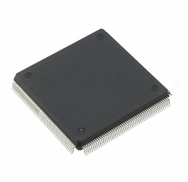


 工商网监
湘ICP备2023018690号
工商网监
湘ICP备2023018690号
