FemtoClock NG Crystal-to-3.3V, 2.5V
Multiple Frequency Clock Generator
w/Fanout Buffer
8T49N028
®
DATA SHEET
General Description
Features
The 8T49N028 is a low RMS phase jitter Clock Synthesizer with
selectable internal crystal oscillator or external clock references and
eight outputs, configurable as either LVDS, LVPECL or High
Impedance.
•
•
Fourth Generation FemtoClock NG PLL technology
•
CLK, nCLK input pair can accept the following differential input
levels: LVPECL, LVDS, HCSL
•
•
FemtoClock NG VCO Range: 1.92GHz - 2.5GHz
•
Clock from OUTPUT DIVIDER A, RMS phase jitter at 156.25MHz
(12KHz - 20MHz): 225fs (typical)
•
Clock from OUTPUT DIVIDER B, RMS phase jitter at 156.25MHz
(12KHz - 20MHz): 219fs (typical)
•
Clock from OUTPUT DIVIDER B, RMS phase jitter at 156.25MHz
(10kHz - 1MHz): 165fs (typical) Full 2.5V or 3.3V power supply
•
•
•
Full 2.5V or 3.3V power supply
•
•
-40°C to 85°C ambient operating temperature
After power up, two frequency select pins determine one of up to four
different sets of factory preprogrammed crystal or input frequency
and output frequency configurations. From a single input reference,
as many as three different output frequencies may be selected for
the output banks: two of these frequencies can be generated by the
internal crystal oscillator, and/or external clock pre-divider, and/or A
output divider, and/or B output divider. The third output frequency is
from the B output divider. Device pre-programming can be
overwritten through the provided I2C interface.
Examples of valid frequency configuration setups illustrate this
device's flexibility, and are shown in Table 3A. The specific internal
register settings for each of the four frequency sets are specified by
an IDT order code. Custom codes can be provided by contacting
IDT.
Eight selectable LVPECL or LVDS outputs (bank selectable, two
output channels per bank)
Bank A and B output frequencies are mux selectable from internal
crystal oscillator, reference clock input, output divider A or output
divider B
I2C programming interface
PCI Express (2.5 Gb/S), Gen 2 (5 Gb/s) and Gen 3 (8 Gb/s) jitter
compliant
Lead-free (RoHS 6) packaging
Q0
nc
SCLK
SDATA
nc
VEE
VCCA
LOCK
VEE
nCLK
CLK
CLK_SEL
VEE
Pin Assignment
48 47 46 45 44 43 42 41 40 39 38 37
36
1
VEE
nQ0
2
35
Q4
Q1
3
34
nQ4
nQ1
4
33
Q5
VCCO_A
5
32
nQ5
nc
6
31
VCCO_C
nc
7
30
VCCO_D
VCCO_B
8
29
Q6
Q2
9
28
nQ6
nQ2
10
27
Q7
Q3
11
26
nQ7
VEE
VEE
FSEL1
VCC
VEE
ADDR_SEL
FSEL0
VCC
VEE
XTAL_OUT
XTAL_IN
nc
25
12
13 14 15 16 17 18 19 20 21 22 23 24
VEE
nQ3
8T49N028
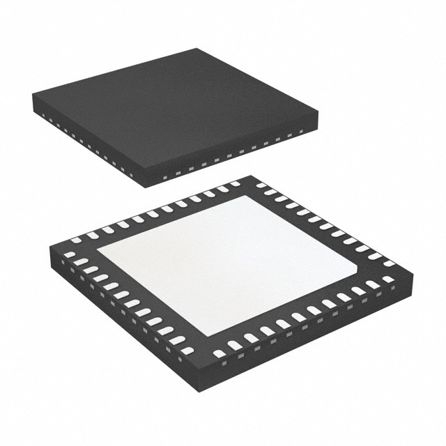
48-pin, 7mm x 7mm VFQFN Package
8T49N028 REVISION 1 10/16/14
1
©2014 Integrated Device Technology, Inc.
�8T49N028 DATA SHEET
Block Diagram
LOCK
PS=x2 Frequency Range:
5MHz to 120MHz;
no limitation for PS=x1 or x0.5
10MHz to
40MHz
CLK SEL
XTAL_IN
XTAL_OUT
CLK
nCLK
Phase Detector
Frequency between
10MHz to 120MHz
P
Pulldown
Pulldown
PU/PD
0
PS
P[1:0]
1
Phase
Detector +
Charge
Pump
VCO Frequency
between
1920MHz to
2500MHz
PNA[1:0]
1
Xtal
OSC
00
01
10
11
NA[5:0]
Q0
nQ0
Bank A
Q1
nQ1
Q2
00
01
10
11
nQ2
Bank B
Q3
nQ3
FemtoClock NG
VCO
2
0
Q4
nQ4
Bank C
Max. Diff.
Input
Frequency:
600MHz
M[7:1]
Q5
NB[6:0]
nQ5
Q6
nQ6
FSEL0
Pulldown
FSEL1
Pulldown
SCLK
Pullup
SDATA
ADDR_SEL
Pullup
Pulldown
REVISION 1 10/16/14
Divider
Mux Selection
Output Type
Output Enable Selection
FEEDBACK DIVIDER 8
OUTPUT DIVIDER B
OUTPUT DIVIDER A
OUTPUT MUX SELECT
OUTPUT STYLE ȸ LVPECL or LVDS
OUTPUT ENABLE
2
Bank D
7
8
4
4
4
Q7
nQ7
FEMTOCLOCK® NG CRYSTAL-TO-3.3V, 2.5V MULTIPLE FREQUENCY
CLOCK GENERATOR W/FANOUT BUFFER
�8T49N028 DATA SHEET
Pin Description and Pin Characteristic Tables
Table 1. Pin Descriptions
Number
Name
Type
Description
1, 2
Q0, nQ0
Output
Differential output pair. LVPECL or LVDS interface levels. (Bank A)
3, 4
Q1, nQ1
Output
Differential output pair. LVPECL or LVDS interface levels. (Bank A)
5
VCCO_A
Power
Output supply pins for Bank A
6, 7,
14, 37, 40
nc
Unused
8
VCCO_B
Power
Output supply pins for Bank B
9, 10
Q2, nQ2
Output
Differential output pair. LVPECL or LVDS interface levels. (Bank B)
No connect.
11, 12
Q3, nQ3
Output
Differential output pair. LVPECL or LVDS interface levels. (Bank B)
13, 17, 21,
24, 25, 36,
41, 44, 48
VEE
ePAD
Power
Negative supply pins. The Thermal Pad must be connected to VEE.
15,
16
XTAL_IN
XTAL_OUT
Input
Crystal oscillator interface. XTAL_IN is the input, XTAL_OUT is the output.
18, 22
VCC
Power
Core supply pins.
Frequency and configuration. Selects between one of four factory
programmable power-up default configurations. The four configurations can
have different PLL states, output frequencies, output styles, multiplexer states
and output states. These default configurations can be overwritten after
power-up via I2C. LVCMOS/LVTTL interface levels.
00 = Configuration 0 (default)
01 = Configuration 1
10 = Configuration 2
11 = Configuration 3
19,
23
FSEL0,
FSEL1
Input
Pulldown
20
ADDR_SEL
Input
Pulldown
26, 27
nQ7, Q7
Output
Differential output pair. LVPECL or LVDS interface levels. (Bank D)
28, 29
nQ6, Q6
Output
Differential output pair. LVPECL or LVDS interface levels. (Bank D)
30
VCCO_D
Power
Output supply pins for Bank D.
31
VCCO_C
Power
Output supply pins for Bank C.
32, 33
nQ5, Q5
Output
Differential output pair. LVPECL or LVDS interface levels. (Bank C)
34, 35
nQ4, Q4
Output
Differential output pair. LVPECL or LVDS interface levels. (Bank C)
38
SCLK
Input
Pullup
I2C Clock Input. LVCMOS/LVTTL interface levels.
39
SDATA
Input/Output
Pullup
I2C Data Input. Input: LVCMOS/LVTTL interface levels. Output: Open Drain.
42
VCCA
Power
Analog supply pin.
43
LOCK
Output
PLL Lock Indicator. LVCMOS/LVTTL interface levels.
45
nCLK
Input
Pullup /
Pulldown
Inverting differential clock input. Internal resistor bias to VCC/2.
46
CLK
Input
Pulldown
Non-inverting differential clock input.
47
CLK_SEL
Input
Pulldown
Input source control pin. LVCMOS/LVTTL interface levels.
0 = XTAL (default)
1 = CLK, nCLK
I2C Address select pin. LVCMOS/LVTTL interface levels.
NOTE: Pullup and Pulldown refer to internal input resistors. See Table 2, Pin Characteristics, for typical values.
REVISION 1 10/16/14
3
FEMTOCLOCK® NG CRYSTAL-TO-3.3V, 2.5V MULTIPLE FREQUENCY
CLOCK GENERATOR W/FANOUT BUFFER
�8T49N028 DATA SHEET
Table 2. Pin Characteristics
Symbol
Parameter
CIN
Input Capacitance
Test Conditions
3.5
pF
RPULLDOWN
Input Pulldown Resistor
51
k
RPULLUP
Input Pullup Resistor
51
k
VCCO_A = VCCO_B = VCCO_C =
VCCO_D = 3.465V
22
VCCO_A = VCCO_B = VCCO_C =
VCCO_D = 2.625V
27
Output Impedance
ROUT
LOCK
Minimum
Typical
Maximum
Units
Frequency Configuration
Table 3A. Frequency Configuration Examples
divA
Frequency
(MHz)
divB
Frequency
(MHz)
Input
Frequency
(MHz)
Input Clock
Divider
P
Input Clock
Prescaler
PS
Feedback
Divider
M
Output
Divider A
PNA x NA
Output
Divider B
NB
VCO
Frequency
(MHz)
100.00
120.00
25.00
1
x2
48
24
20
2400.00
100.00
125.00
25.00
1
x2
50
25
20
2500.00
100.00
156.25
25.00
1
x2
50
25
16
2500.00
100.00
150.00
25.00
1
x2
48
24
16
2400.00
100.00
250.00
25.00
1
x2
50
25
10
2500.00
100.00
312.50
25.00
1
x2
50
25
8
2500.00
100.00
400.00
25.00
1
x2
48
24
6
2400.00
100.00
500.00
25.00
1
x2
50
25
5
2500.00
100.00
625.00
25.00
1
x2
50
25
4
2500.00
125.00
75.00
25.00
1
x1
90
18
30
2250.00
125.00
156.25
25.00
1
x2
50
20
16
2500.00
125.00
187.50
25.00
1
x1
90
18
12
2250.00
125.00
200.00
25.00
1
x2
40
16
10
2000.00
125.00
250.00
25.00
1
x2
40
16
8
2000.00
125.00
312.50
25.00
1
x2
50
20
8
2500.00
125.00
400.00
25.00
1
x2
40
16
5
2000.00
125.00
500.00
25.00
1
x2
50
20
5
2500.00
125.00
625.00
25.00
1
x2
50
20
4
2500.00
30.72
122.88
19.20
1
x2
64
80
20
2457.60
30.72
153.60
19.20
1
x2
64
80
16
2457.60
122.88
153.60
19.20
1
x2
64
20
16
2457.60
122.88
491.52
19.20
1
x2
64
20
5
2457.60
153.60
491.52
19.20
1
x2
64
16
5
2457.60
155.52
622.08
19.44
1
x2
64
16
4
2488.32
19.20
153.60
30.72
1
x2
40
128
16
2457.60
153.60
491.52
30.72
1
x2
40
16
5
2457.60
NOTE:
NOTE:
Each device supports four output frequencies (with related input or crystal value) as selected from this Register Settings Table.
XTAL operation: Using divA fOUT = fREF * PS * [M / (NA x PNA)].
Using divB fOUT = fREF / P * PS * [M / (NA x PNA)].
Using divB fOUT = fREF / P * PS * M / NB.
REVISION 1 10/16/14
4
FEMTOCLOCK® NG CRYSTAL-TO-3.3V, 2.5V MULTIPLE FREQUENCY
CLOCK GENERATOR W/FANOUT BUFFER
�8T49N028 DATA SHEET
Table 3B. I2C Register Map
Register
Binary
Register
Address
Register Bit
D7
D6
D5
D4
D3
D2
D1
D0
0
00000
0
M0[7]
M0[6]
M0[5]
M0[4]
M0[3]
M0[2]
M0[1]
1
00001
0
M1[7]
M1[6]
M1[5]
M1[4]
M1[3]
M1[2]
M1[1]
2
00010
0
M2[7]
M2[6]
M2[5]
M2[4]
M2[3]
M2[2]
M2[1]
3
00011
0
M3[7]
M3[6]
M3[5]
M3[4]
M3[3]
M3[2]
M3[1]
4
00100
0
NB0[6]
NB0[5]
NB0[4]
NB0[3]
NB0[2]
NB0[1]
NB0[0]
5
00101
0
NB1[6]
NB1[5]
NB1[4]
NB1[3]
NB1[2]
NB1[1]
NB1[0]
6
00110
0
NB2[6]
NB2[5]
NB2[4]
NB2[3]
NB2[2]
NB2[1]
NB2[0]
7
00111
0
NB3[6]
NB3[5]
NB3[4]
NB3[3]
NB3[2]
NB3[1]
NB3[0]
8
01000
BYPASS0
PS0[1]
PS0[0]
P0[1]
P0[0]
CP0[1]
CP0[0]
9
01001
BYPASS1
PS1[1]
PS1[0]
P1[1]
P1[0]
CP1[1]
CP1[0]
10
01010
BYPASS2
PS2[1]
PS2[0]
P2[1]
P2[0]
CP2[1]
CP2[0]
11
01011
BYPASS3
PS3[1]
PS3[0]
P3[1]
P3[0]
CP3[1]
CP3[0]
12
01100
OED0
OEC0
OEB0
OEA0
LVDS_
SELD0
LVDS_
SELC0
LVDS_
SELB0
LVDS_
SELA0
13
01101
OED1
OEC1
OEB1
OEA1
LVDS_
SELD1
LVDS_
SELC1
LVDS_
SELB1
LVDS_
SELA1
14
01110
OED2
OEC2
OEB2
OEA2
LVDS_
SELD2
LVDS_
SELC2
LVDS_
SELB2
LVDS_
SELA2
15
01111
OED3
OEC3
OEB3
OEA3
LVDS_
SELD3
LVDS_
SELC3
LVDS_
SELB3
LVDS_
SELA3
16
10000
0
0
0
0
MUXB0[1]
MUXB0[0]
MUXA0[1]
MUXA0[0]
17
10001
0
0
0
0
MUXB1[1]
MUXB1[0]
MUXA1[1]
MUXA1[0]
18
10010
0
0
0
0
MUXB2[1]
MUXB2[0]
MUXA2[1]
MUXA2[0]
19
10011
0
0
0
0
MUXB3[1]
MUXB3[0]
MUXA3[1]
MUXA3[0]
20
10100
PNA0[1]
PNA0[0]
NA0[5]
NA0[4]
NA0[3]
NA0[2]
NA0[1]
NA0[0]
21
10101
PNA1[1]
PNA1[0]
NA1[5]
NA1[4]
NA1[3]
NA1[2]
NA1[1]
NA1[0]
22
10110
PNA2[1]
PNA2[0]
NA2[5]
NA2[4]
NA2[3]
NA2[2]
NA2[1]
NA2[0]
23
10111
PNA3[1]
PNA3[0]
NA3[5]
NA3[4]
NA3[3]
NA3[2]
NA3[1]
NA3[0]
NOTE: OEx, LVDS_SELx registers control the Output Bank State and not the Individual Output Channel State.
REVISION 1 10/16/14
5
FEMTOCLOCK® NG CRYSTAL-TO-3.3V, 2.5V MULTIPLE FREQUENCY
CLOCK GENERATOR W/FANOUT BUFFER
�8T49N028 DATA SHEET
Table 3C. I2C Function Descriptions
Bits
Name
Mn[7:1]
Integer Feedback Divider
Register n
(n = 0...3)
Sets the integer feedback divider value. Based on the FemtoClock NG
VCO range, the applicable feedback dividers settings are 16 thru 250.
Please note the register value presents bits [7:1] of Mn, the LSB of Mn is
not in the register. Mn[7:1] bits are programmed with values to support
default configuration settings for FSEL[1:0].
NBn[6:0]
Output Divider Register B n
(n = 0...3)
Sets the output divider B. The output divider value can range from 2, 3, 4,
5, 6 and 8, 10, 12 to 126 (step: 2). See Table 3I for the output divider
coding. NBn[6:0] bits are programmed with values to support default
configuration settings for FSEL[1:0].
BYPASSn
PLL Bypass Register n
(n = 0...3)
Bypasses PLL Output of the prescaler is routed through the output divider
N to the output fanout buffer. Programming a 1 to this bit bypasses the
PLL. Programming a 0 to this bit routes the output of the prescaler
through the PLL. BYPASSn bits are programmed with values to support
default configuration setting for FSEL[1:0]
PSn(1:0)
Input Prescaler Register n
(n = 0...3)
Sets the PLL input clock prescaler value. Valid prescaler values are x0.5,
x1 or x2. See Table 3E. Set prescaler to x2 for optimum phase noise
performance. PSn[1:0] bits are programmed with values to support default
configuration settings for FSEL[1:0].
Pn[1:0]
Input Clock Divider Register n
(n = 0...3)
Sets the PLL input clock divider. The divider value has the range of 1, 2,
4 and 5. See Table 3E. Pn[1:0] bits are programmed with values to support
default configuration settings for FSEL[1:0].
CPn[1:0]
PLL Bandwidth Register n
(n = 0...3)
Sets the FemtoClock NG PLL bandwidth by controlling the charge pump
current. See Table 3J. CPn[1:0] bits are programmed with values to
support default configuration settings for FSEL[1:0].
Output Enable Register n
(n = 0...3)
Sets the outputs to Active or High Impedance. Programming a 0 to this
bit sets the outputs to High Impedance. Programming a 1 sets the
outputs to active status. OEAn(Bank A), OEBn(Bank B), OECn(Bank
C), OEDn(Bank D) bits are programmed with values to support default
configuration settings for FSEL[1:0].
OEAn
OEBn
OECn
OEDn
Function
LVDS_SELAn
LVDS_SELBn
LVDS_SELCn
LVDS_SELDn
Output Style Register n
(n = 0...3)
Sets the differential output style to either LVDS or LVPECL interface
levels. Programming a 1 to this bit sets the output styles to LVDS levels.
Programming a 0 to this bit sets the output styles to LVPECL levels.
LVDS_SELAn(Bank A), LVDS_SELBn(Bank B), LVDS_SELCn (Bank C),
LVDS_SELDn(Bank D) bits are programmed with values to support
default configuration settings for FSEL[1:0].
MUXAn[1:0]
MUXBn[1:0]
MUX Select Register n
(n = 0...3)
Sets the multiplexer input to either Crystal Input, Reference Clock Input,
Divider A, or Divider B. See Tables 3K and 3L.
MUXAn[1:0], MUXBn[1:0] bits are programmed with values to support
default configuration settings for FSEL[1:0].
PNAn[1:0]
Output Pre-Divider Register A
n
(n = 0...3)
Sets the pre output divider A. The output divider value are 2, 3, or 5. See
Table 3F for the output divider coding. PNAn[1:0] bits are programmed
with values to support default configuration settings for FSEL[1:0].
NAn[5:0]
Output Divider Register A n
(n = 0...3)
Sets the output divider A. The output divider value can range from 1 to 63.
See Table 3G for the output divider coding. NAn[5:0] bits are programmed
with values to support default configuration settings for FSEL[1:0].
REVISION 1 10/16/14
6
FEMTOCLOCK® NG CRYSTAL-TO-3.3V, 2.5V MULTIPLE FREQUENCY
CLOCK GENERATOR W/FANOUT BUFFER
�8T49N028 DATA SHEET
Table 3D. PLL Frequency Range Setting
Table 3G. PLL Output Divider NA Coding
Frequency Range (MHz)
Register Bit
Phase Detector
10 – 120
NAx[5:0]
Output Divider N
x2 Circuitry (PS)
5 – 120
000000
n/a
000001
n/a
000010
2
000011
3
Feedback Divider Mx
000100
4
Do Not Use
1 thru 15
000101
5
00001000
16
000110
6
00001001
18
000111
7
00001010
20
001000
8
22
001001
9
…
001010
10
01111100
248
001011
11
01111101
250
Table 3E. Feedback Divider Mn Coding
Register Bit
Mx[8:1]
00001011
…
…
111111
…
63
Table 3F. PLL Pre Output Divider PNA Coding
Register Bit
PNAx[1:0]
Pre Output Divider A
PNA
00
2
01
3
10
5
11
2
REVISION 1 10/16/14
7
FEMTOCLOCK® NG CRYSTAL-TO-3.3V, 2.5V MULTIPLE FREQUENCY
CLOCK GENERATOR W/FANOUT BUFFER
�8T49N028 DATA SHEET
Table 3H. PLL Output Divider PNA and NA Coding
Register Bit
Register Bit
PNAn[1:0]
NAn[5:0]
Output Divider
fOUT_MIN (MHz)
fOUT_MAX (MHz)
00
000000
n/a
n/a
n/a
00
000001
n/a
n/a
n/a
00
000010
4
480.00
625.00
NAn * 2
(960 ÷ NAn)
(1250 ÷ NAn)
00
Output Frequency Range
…
00
111111
126
15.24 (approx.)
19.84 (approx.)
01
000000
n/a
n/a
n/a
01
000001
n/a
n/a
n/a
01
000010
6
320.00
416.67
NAn * 3
(640 ÷ NAn)
(833.33 ÷ NAn)
01
01
111111
…
189
10.16 (approx.)
13.23 (approx.)
10
000000
n/a
n/a
n/a
10
000001
n/a
n/a
n/a
10
000010
10
…
10
192.00
250.00
NAn * 5
(384 ÷ NAn)
(500 ÷ NAn)
10
111111
315
6.10 (approx.)
7.94 (approx.)
11
000000
n/a
n/a
n/a
11
000001
n/a
n/a
n/a
11
000010
4
480.00
625.00
NAn * 2
(960 ÷ NAn)
(1250 ÷ NAn)
126
15.24 (approx.)
19.84 (approx.)
11
…
11
111111
Table 3I. PLL Output Divider NB Coding
Register Bit
Output Frequency Range
NBn[6:0]
Output Divider N
000000X
n/a
0000010
2
960.00
1250.00
0000011
3
640.00
833.33
0000100
4
480.00
625.00
0000101
5
384.00
500.00
000011X
6
320.00
416.67
000100X
8
240.00
312.5
000101X
10
192.00
250.00
000110X
12
160.00
208.33
000111X
14
137.14 (approx.)
178.57 (approx.)
001000X
fOUT_MIN (MHz)
fOUT_MAX (MHz)
n/a
16
120.00
156.25
NB (even integer)
(1920 ÷ NBn)
(2500 ÷ NBn)
111101X
124
15.48 (approx.)
20.16 (approx.)
111111X
126
15.24 (approx.)
19.84 (approx.)
…
NOTE: X denotes “don’t care”.
REVISION 1 10/16/14
8
FEMTOCLOCK® NG CRYSTAL-TO-3.3V, 2.5V MULTIPLE FREQUENCY
CLOCK GENERATOR W/FANOUT BUFFER
�8T49N028 DATA SHEET
Table 3J. FemtoClock NG PLL Bandwidth Coding
Table 3K. MUXAn (n = 0...3) Clock Source
Feedback Divider
Value Range (MHz)
Register Bit
Register Bit
MUXA[1]
MUXA[0]
Selected
Clock Source
CPn1
CPn0
Minimum
Maximum
0
0
Crystal Input
0
0
16
48
0
1
CLK, nCLK
0
1
48
100
1
0
Output Divider A
1
0
100
250
1
1
Output Divider B
1
1
192
250
NOTE: FemtoClock NG PLL stability is only guaranteed over the
feedback divider ranges listed is Table 3F, 3G, 3H, 3I and 3J.
Table 3L. Bank B MUXn Clock Source
Register Bit
MUXB[1]
MUXB[0]
Selected
Clock Source
0
0
Crystal Input
0
1
CLK, nCLK
1
0
Output Divider A
1
1
Output Divider B
REVISION 1 10/16/14
9
FEMTOCLOCK® NG CRYSTAL-TO-3.3V, 2.5V MULTIPLE FREQUENCY
CLOCK GENERATOR W/FANOUT BUFFER
�8T49N028 DATA SHEET
Power-up Default Configuration Description
The 8T49N028 supports a variety of options such as different output
styles, number of programmed default frequencies, output enable
and operating temperature range. The device options and default
frequencies must be specified at the time of order and are
programmed by IDT prior to shipment. The document,
Programmable FemtoClock® Ordering Product Information specifies
the available order codes, including the device options and default
frequency configurations. Example part number:
8T49N028-001NLGI, specifies a quad frequency clock generator
with default frequencies of 25MHz, 100MHz, 156.25MHz and
156.25MHz, with four LVPECL outputs that are enabled after
power-up, specified over the industrial temperature range and
housed in a lead-free (6/6 RoHS) VFQFN package.
Other order codes with respective programmed frequencies are
available from IDT upon request. After power-up changes to the
output frequencies are controlled by FSEL[1:0] or the I2C interface.
Changes to the output styles and states of outputs (enabled or
disabled) can also be controlled with the I2C interface after power up.
Table 3M. Power-up Default Settings
FSEL1
FSEL0
Frequency Set
PLL State
(On or Bypass)
Output State
(Active or High Impedance)
Output Style
(LVDS or LVPECL)
0 (default)
0 (default)
Frequency Set 0
PLL State 0
Output State 0
Output Style 0
0
1
Frequency Set 1
PLL State 1
Output State 1
Output Style 1
1
0
Frequency Set 2
PLL State 2
Output State 2
Output Style 2
1
1
Frequency Set 3
PLL State 3
Output State 3
Output Style 3
Serial Interface Configuration Description
The 8T49N028 has an I2C-compatible configuration interface to
access any of the internal registers (Table 3B) for frequency and PLL
parameter programming. The 8T49N028 acts as a slave device on
the I2C bus and has the address 0b110111x, where x is set by the
value on the ADDR_SEL input (see Tables 3N and 3O). The interface
accepts byte-oriented block write and block read operations. An
address byte (P) specifies the register address (Table 3B) as the byte
position of the first register to write or read. Data bytes (registers) are
accessed in sequential order from the lowest to the highest byte
(most significant bit first, see Tables 3P, and 3Q). Read and write
block transfers can be stopped after any complete byte transfer. It is
recommended to terminate the I2C read or write transfer after
accessing byte #23 by sending a stop command.
For full electrical I2C compliance, it is recommended to use external
pull-up resistors for SDATA and SCLK. The internal pull-up resistors
have a size of 50k typical.
Table 3N. I2C Device Slave Address ADDR_SEL = 0 (default)
1
1
0
1
1
1
0
R/W
Table 3O. I2C Device Slave Address ADDR_SEL = 1
1
1
0
1
1
1
1
R/W
Table 3P. Block Write Operation
Bit
Description
1
2:8
9
10
11:18
19
20:27
28
29-36
37
...
...
...
START
Slave Address
W (0)
ACK
Address Byte P
ACK
Data Byte
(P)
ACK
Data Byte
(P+1)
ACK
Data Byte
...
ACK
STOP
1
7
1
1
8
1
8
1
8
1
8
1
1
Length (bits)
Table 3Q. Block Read Operation
Bit
1
Description
Length (bits)
2:8
9
10
11:18
19
Address
byte P
A
C
K
Repeated
START
8
1
1
START
Slave
Address
W
(0)
A
C
K
1
7
1
1
REVISION 1 10/16/14
20
21:27
28
29
30:37
38
39-46
47
...
...
...
Slave
address
R
(1)
A
C
K
Data Byte
(P)
A
C
K
Data Byte
(P+1)
A
C
K
Data Byte
...
A
C
K
STOP
7
1
1
8
1
8
1
8
1
1
10
FEMTOCLOCK® NG CRYSTAL-TO-3.3V, 2.5V MULTIPLE FREQUENCY
CLOCK GENERATOR W/FANOUT BUFFER
�8T49N028 DATA SHEET
Absolute Maximum Ratings
NOTE: Stresses beyond those listed under Absolute Maximum Ratings may cause permanent damage to the device. These ratings are stress
specifications only. Functional operation of the product at these conditions or any conditions beyond those listed in the DC Characteristics or
AC Characteristics is not implied. Exposure to absolute maximum rating conditions for extended periods may affect product reliability.
Item
Rating
Supply Voltage, VCC
3.63V
Inputs, VI
XTAL_IN
Other Input
0V to 2V
-0.5V to VCC + 0.5V
Outputs, VO (LVCMOS)
-0.5V to VCCO_x + 0.5V
Outputs, IO (LVPECL)
Continuous Current
Surge Current
50mA
100mA
Outputs, IO (SDATA)
10mA
Outputs, IO (LVDS)
Continuous Current
Surge Current
10mA
15mA
Junction Temperature, TJ
125°C
Storage Temperature, TSTG
-65C to 150C
NOTE: VCCO_X denotes VCCO_A + VCCO_B + VCCO_C + VCCO_D.
DC Electrical Characteristics
Table 4A. Power Supply DC Characteristics, VCC = VCCO_x = 3.3V ± 5%, VEE = 0V, TA = -40°C to 85°C
Symbol
Parameter
VCC
Core Supply Voltage
VCCA
Test Conditions
Minimum
Typical
Maximum
Units
3.135
3.3
3.465
V
Analog Supply Voltage
VCC – 0.062
3.3
VCC
V
VCCO_x
Output Supply Voltage
3.135
3.3
3.465
V
ICCA
Analog Supply Current
27
31
mA
IEE
Power Supply Current
LVPECL
250
286
mA
ICC
Power Supply Current
LVDS
164
188
mA
ICCO_x
Output Supply Current
LVDS
140
162
mA
NOTE: VCCO_X denotes VCCO_A + VCCO_B + VCCO_C + VCCO_D.
Table 4B. Power Supply DC Characteristics, VCC = VCCO_x = 2.5V ± 5%, VEE = 0V, TA = -40°C to 85°C
Symbol
Parameter
VCC
Core Supply Voltage
VCCA
Test Conditions
Minimum
Typical
Maximum
Units
2.375
2.5
2.625
V
Analog Supply Voltage
VCC – 0.054
2.5
VCC
V
2.375
2.5
2.625
V
23
27
mA
VCCO_x
Output Supply Voltage
ICCA
Analog Supply Current
IEE
Power Supply Current
LVPECL
245
276
mA
ICC
Power Supply Current
LVDS
160
180
mA
ICCO
Output Supply Current
LVDS
140
161
mA
NOTE: VCCO_X denotes VCCO_A + VCCO_B + VCCO_C + VCCO_D.
REVISION 1 10/16/14
11
FEMTOCLOCK® NG CRYSTAL-TO-3.3V, 2.5V MULTIPLE FREQUENCY
CLOCK GENERATOR W/FANOUT BUFFER
�8T49N028 DATA SHEET
Table 4C. LVCMOS/LVTTL DC Characteristics, VCC = VCCO_x = 3.3V ± 5% or 2.5V ± 5%, VEE = 0V, TA = -40°C to 85°C
Symbol
Parameter
VIH
Input High
Voltage
VIL
Input Low
Voltage
SCLK, SDATA,
FSEL[1:0],
CLK_SEL,
ADDR_SEL
SCLK, SDATA,
CLK_SEL,
ADDR_SEL
FSEL[1:0],
IIH
IIL
Input
High Current
Input
Low Current
Test Conditions
Minimum
VCC = 3.3V
Typical
Maximum
Units
2
VCC + 0.3
V
VCC = 2.5V
1.7
VCC + 0.3
V
VCC = 3.3V
-0.3
0.8
V
VCC = 2.5V
-0.3
0.7
V
VCC = 3.3V or 2.5V
-0.3
0.5
V
SCLK, SDATA
VCC = VIN = 3.465V or 2.625V
5
µA
FSEL[1:0],
CLK_SEL,
ADDR_SEL
VCC = VIN = 3.465V or 2.625V
150
µA
SCLK, SDATA
VCC = 3.465V or 2.625V,
VIN = 0V
-150
µA
FSEL[1:0],
CLK_SEL,
ADDR_SEL
VCC = 3.465V or 2.625V,
VIN = 0V
-5
µA
VOH
Output High
LOCK
Voltage; NOTE 1
VCCO_x = 3.465V
2.6
V
VCCO_x = 2.625V
1.8
V
VOL
Output Low
LOCK
Voltage; NOTE 1
VCCO_x = 3.465V or 2.625V
0.7
V
NOTE: VCCO_X denotes VCCO_A + VCCO_B + VCCO_C + VCCO_D.
NOTE 1: Output terminated with 50 to VCCO_x/2. See Parameter Measurement Information, Output Load Test Circuit diagrams.
Table 4D. Differential DC Characteristics, VCC = VCCO_x = 3.3V ± 5% or 2.5V ± 5%, VEE = 0V, TA = -40°C to 85°C
Symbol
Parameter
Test Conditions
IIH
Input
High Current
IIL
Input
Low Current
VPP
Peak-to-Peak Voltage
0.2
1.3
V
VCMR
Common Mode Input Voltage;
NOTE 1
VEE
VCC – 1.0
V
CLK, nCLK
Minimum
Typical
VCC = VIN = 3.465V or 2.625V
Maximum
Units
150
µA
nCLK
VCC = 3.465V or 2.625V, VIN = 0V
-150
µA
CLK
VCC = 3.465V or 2.625V, VIN = 0V
-5
µA
NOTE: VCCO_X denotes VCCO_A + VCCO_B + VCCO_C + VCCO_D.
NOTE 1: Common mode input voltage is at the cross point.
Table 4E. LVPECL DC Characteristics, VCC = VCCO_x = 3.3V±5%, VEE = 0V, TA = -40°C to 85°C
Symbol
Parameter
VOH
Output High Voltage; NOTE 1
VOL
Output Low Voltage; NOTE 1
VSWING
Peak-to-Peak Output Voltage Swing
Test Conditions
Minimum
Typical
Maximum
Units
VCCO_x – 1.1
VCCO_x – 0.75
V
VCCO_x – 2.0
VCCO_x – 1.6
V
0.6
1.0
V
NOTE: VCCO_X denotes VCCO_A + VCCO_B + VCCO_C + VCCO_D.
NOTE 1: Outputs termination with 50 to VCCO_x – 2V.
REVISION 1 10/16/14
12
FEMTOCLOCK® NG CRYSTAL-TO-3.3V, 2.5V MULTIPLE FREQUENCY
CLOCK GENERATOR W/FANOUT BUFFER
�8T49N028 DATA SHEET
Table 4F. LVPECL DC Characteristics, VCC = VCCO_x = 2.5V ± 5%, VEE = 0V, TA = -40°C to 85°C
Symbol
Parameter
Test Conditions
Minimum
Typical
Maximum
Units
VOH
Output High Voltage; NOTE 1
VCCO_x – 1.2
VCCO_x – 0.75
V
VOL
Output Low Voltage; NOTE 1
VCCO_x – 2.0
VCCO_x – 1.5
V
VSWING
Peak-to-Peak Output Voltage
Swing
0.5
1.0
V
NOTE: VCCO_X denotes VCCO_A + VCCO_B + VCCO_C + VCCO_D.
NOTE 1: Outputs termination with 50 to VCC – 2V.
Table 4G. LVDS DC Characteristics, VCC = VCCO_x = 3.3V±5%, VEE = 0V, TA = -40°C to 85°C
Symbol
Parameter
VOD
Differential Output Voltage
VOD
VOD Magnitude Change
VOS
Offset Voltage
VOS
VOS Magnitude Change
Test Conditions
Minimum
Typical
Maximum
Units
247
340
454
mV
50
mV
1.125
1.25
1.375
V
50
mV
NOTE: VCCO_X denotes VCCO_A + VCCO_B + VCCO_C + VCCO_D.
Table 4H. LVDS DC Characteristics, VCC = VCCO_x = 2.5V ± 5%, VEE = 0V, TA = -40°C to 85°C
Symbol
Parameter
VOD
Differential Output Voltage
VOD
VOD Magnitude Change
VOS
Offset Voltage
VOS
VOS Magnitude Change
Test Conditions
Minimum
Typical
Maximum
Units
247
335
454
mV
50
mV
1.125
1.25
1.375
V
50
mV
NOTE: VCCO_X denotes VCCO_A + VCCO_B + VCCO_C + VCCO_D.
Table 5. Crystal Characteristics
Parameter
Test Conditions
Minimum
Mode of Oscillation
Typical
Maximum
Units
Fundamental
Frequency
10
40
MHz
Load Capacitance (CL)
12
18
pF
50
Equivalent Series Resistance (ESR)
REVISION 1 10/16/14
13
FEMTOCLOCK® NG CRYSTAL-TO-3.3V, 2.5V MULTIPLE FREQUENCY
CLOCK GENERATOR W/FANOUT BUFFER
�8T49N028 DATA SHEET
AC Electrical Characteristics
Table 6A. PCI Express Jitter Specifications, VCC = VCCO_x = 3.3V ± 5% or 2.5V ± 5%, VEE = 0V, TA = -40°C to 85°C
Typical
Maximum
PCIe Industry
Specification
Units
Output Divider A,
ƒ = 100MHz, 25MHz Crystal Input
Evaluation Band: 0Hz - Nyquist
(clock frequency/2)
8
12
86
ps
Phase Jitter
RMS; NOTE 2, 4
Output Divider A,
ƒ = 100MHz, 25MHz Crystal Input
High Band: 1.5MHz - Nyquist
(clock frequency/2)
0.8
1.3
3.1
ps
tREFCLK_LF_RMS
(PCIe Gen 2)
Phase Jitter
RMS; NOTE 2, 4
Output Divider A,
ƒ = 100MHz, 25MHz Crystal Input
Low Band: 10kHz - 1.5MHz
0.03
0.06
3.0
ps
tREFCLK_RMS
(PCIe Gen 3)
Phase Jitter
RMS;
NOTE 3, 4
Output Divider A,
ƒ = 100MHz, 25MHz Crystal Input
Evaluation Band: 0Hz - Nyquist
(clock frequency/2)
0.17
0.32
0.8
ps
Symbol
Parameter
tj
(PCIe Gen 1)
Phase Jitter
Peak-to-Peak;
NOTE 1, 4
tREFCLK_HF_RMS
(PCIe Gen 2)
Test Conditions
Minimum
NOTE: Electrical parameters are guaranteed over the specified ambient operating temperature range, which is established when the device is
mounted in a test socket with maintained transverse airflow greater than 500 lfpm. The device will meet specifications after thermal equilibrium
has been reached under these conditions. For additional information, refer to the PCI Express Application Note section in the datasheet.
NOTE: VCCO_X denotes VCCO_A + VCCO_B + VCCO_C + VCCO_D.
NOTE 1: Peak-to-Peak jitter after applying system transfer function for the Common Clock Architecture. Maximum limit for PCI Express Gen 1
is 86ps peak-to-peak for a sample size of 106 clock periods.
NOTE 2: RMS jitter after applying the two evaluation bands to the two transfer functions defined in the Common Clock Architecture and
reporting the worst case results for each evaluation band. Maximum limit for PCI Express Generation 2 is 3.1ps RMS for tREFCLK_HF_RMS
(High Band) and 3.0ps RMS for tREFCLK_LF_RMS (Low Band).
NOTE 3: RMS jitter after applying system transfer function for the common clock architecture. This specification is based on the PCI Express
Base Specification Revision 0.7, October 2009 and is subject to change pending the final release version of the specification.
NOTE 4: This parameter is guaranteed by characterization. Not tested in production.
REVISION 1 10/16/14
14
FEMTOCLOCK® NG CRYSTAL-TO-3.3V, 2.5V MULTIPLE FREQUENCY
CLOCK GENERATOR W/FANOUT BUFFER
�8T49N028 DATA SHEET
Table 6B. AC Characteristics, VCC = VCCO_x = 3.3V ± 5% or 2.5V ± 5% VEE = 0V, TA = -40°C to 85°C
Symbol
Parameter
fDIFF_IN
Differential Input Frequency;
NOTE 1
fVCO
VCO Frequency
tjit(Ø)
RMS Phase Jitter (Random);
NOTE 2
25MHz Crystal, fOUT = 25MHz,
Integration Range: 1kHz – 1MHz
tjit(Ø)
RMS Phase Jitter (Random);
NOTE 2
tjit(Ø)
tjit(Ø)
tsk(o)
tsk(b)
Test Conditions
Typical
Maximum
Units
600
MHz
2500
MHz
170
209
fs
25MHz Crystal, fOUT = 25MHz,
Integration Range: 12kHz – 5MHz
321
268
fs
25MHz Crystal, fOUT = 100MHz,
Integration Range: 12kHz – 20MHz
299
376
fs
25MHz Crystal, fOUT = 125MHz,
Integration Range: 12kHz – 20MHz
296
390
fs
25MHz Crystal, fOUT = 156.25MHz,
Integration Range: 12kHz – 20MHz
225
301
fs
25MHz Crystal, fOUT = 156.25MHz,
Integration Range: 10kHz – 1MHz
166
189
fs
25MHz Crystal, fOUT = 250MHz,
Integration Range: 12kHz – 20MHz
259
322
fs
30.72MHz Crystal, fOUT = 491.52MHz,
Integration Range: 12kHz – 20MHz
182
234
fs
19.44MHz Crystal, fOUT = 622.08MHz,
Integration Range: 12kHz – 20MHz
330
415
fs
25MHz Crystal, fOUT = 100MHz,
Integration Range: 12kHz – 20MHz
240
270
fs
25MHz Crystal, fOUT = 125MHz,
Integration Range: 12kHz – 20MHz
228
273
fs
25MHz Crystal, fOUT = 156.25MHz,
Integration Range: 12kHz – 20MHz
219
257
fs
25MHz Crystal, fOUT = 156.25MHz,
Integration Range: 10kHz – 1MHz
165
193
fs
25MHz Crystal, fOUT = 250MHz,
Integration Range: 12kHz – 20MHz
210
251
fs
30.72MHz Crystal, fOUT = 491.52MHz,
Integration Range: 12kHz – 20MHz
171
204
fs
19.44MHz Crystal, fOUT = 622.08MHz,
Integration Range: 12kHz – 20MHz
320
403
fs
1920
RMS Phase Jitter, Random;
Output Divider A
Output Bank A,B
NOTE 2
RMS Phase Jitter, Random;
Output Divider B,
Output Bank C,D
NOTE 2
Output Skew;
NOTE 3, 4
Minimum
LVPECL
Outputs
LVDS_SEL = 0
130
ps
LVDS
Outputs
LVDS_SEL = 1
100
ps
LVPECL
Outputs
LVDS_SEL = 0
40
ps
LVDS
Outputs
LVDS_SEL = 1
30
ps
Bank Skew
REVISION 1 10/16/14
15
FEMTOCLOCK® NG CRYSTAL-TO-3.3V, 2.5V MULTIPLE FREQUENCY
CLOCK GENERATOR W/FANOUT BUFFER
�8T49N028 DATA SHEET
Symbol
tR / tF
odc
Parameter
Output
Rise/Fall Time
Test Conditions
Minimum
Typical
Maximum
Units
LVPECL
Outputs
20% - 80%, LVDS_SEL = 0
250
600
ps
LVDS
Outputs
20% - 80%, LVDS_SEL = 1
270
500
ps
Output Divider N 3;
LVDS_SEL = 0 or 1
47
53
%
Output Divider N = 3;
LVDS_SEL = 0 or 1
45
55
%
Output Duty Cycle
tLOCK
PLL Lock Time;
NOTE 4, 5
LOCK
Output
20
ms
tTRANSITION
Transition
Time;
NOTE 4, 5
LOCK
Output
20
ms
NOTE: VCCO_X denotes VCCO_A + VCCO_B + VCCO_C + VCCO_D.
NOTE: Electrical parameters are guaranteed over the specified ambient operating temperature range, which is established when the device is
mounted in a test socket with maintained transverse airflow greater than 500 lfpm. The device will meet specifications after thermal equilibrium
has been reached under these conditions.
NOTE 1: The input frequency of the differential input is a physical limitation of the device. Follow the PLL setting to insure proper functionality
of the device.
NOTE 2: Refer to Phase Noise Plots.
NOTE 3: Defined as skew between outputs at the same supply voltage and with equal load conditions. Measured at the differential cross
points.
NOTE 4: These parameters are guaranteed by characterization. Not tested in production.
NOTE 5: Refer to tLOCK and tTRANSITION in Parameter Measurement Information.
REVISION 1 10/16/14
16
FEMTOCLOCK® NG CRYSTAL-TO-3.3V, 2.5V MULTIPLE FREQUENCY
CLOCK GENERATOR W/FANOUT BUFFER
�8T49N028 DATA SHEET
Noise Power (dBc/Hz)
Typical Phase Noise at 156.25MHz
Offset Frequency (Hz)
REVISION 1 10/16/14
17
FEMTOCLOCK® NG CRYSTAL-TO-3.3V, 2.5V MULTIPLE FREQUENCY
CLOCK GENERATOR W/FANOUT BUFFER
�8T49N028 DATA SHEET
Parameter Measurement Information
2V
2V
2V
VCC,
VCCO_x
2V
Qx
SCOPE
VCC,
VCCO_x
VCCA
Qx
VCCA
nQx
nQx
-1.3V± 0.165V
-0.5V ± 0.125V
VCCO_X denotes VCCO_A + VCCO_B + VCCO_C + VCCO_D
VCCO_X denotes VCCO_A + VCCO_B + VCCO_C + VCCO_D
2.5V LVPECL Output Load Test Circuit
3.3V LVPECL Output Load Test Circuit
3.3V ±5%
SCOPE
VCC,
VCCO_x
SCOPE
2.5V±5%
POWER SUPPLY
+ Float GND –
VCCA
VCC,
VCCO_x
VCCA
Qx
nQx
VCCO_X denotes VCCO_A + VCCO_B + VCCO_C + VCCO_D
VCCO_X denotes VCCO_A + VCCO_B + VCCO_C + VCCO_D
2.5V LVDS Output Load Test Circuit
3.3V LVDS Output Load Test Circuit
VCC
nCLK
CLK
VEE
RMS Phase Jitter
Differential Input Levels
REVISION 1 10/16/14
18
FEMTOCLOCK® NG CRYSTAL-TO-3.3V, 2.5V MULTIPLE FREQUENCY
CLOCK GENERATOR W/FANOUT BUFFER
�8T49N028 DATA SHEET
Parameter Measurement Information, continued
nQ[0:7]
nQx
Q[0:7]
Qx
nQy
Qy
Output Duty Cycle/Pulse Width/Period
Output Skew
nQ[0:7]
nQ[0:7]
80%
80%
VOD
Q[0:7]
Q[0:7]
20%
20%
tR
LVPECL Output Rise/Fall Time
LVDS Output Rise/Fall Time
Offset Voltage Setup
Differential Output Voltage Setup
REVISION 1 10/16/14
19
tF
FEMTOCLOCK® NG CRYSTAL-TO-3.3V, 2.5V MULTIPLE FREQUENCY
CLOCK GENERATOR W/FANOUT BUFFER
�8T49N028 DATA SHEET
Parameter Measurement Information, continued
tsk(b)
Bank Skew
Lock Time & Transition Time
REVISION 1 10/16/14
20
FEMTOCLOCK® NG CRYSTAL-TO-3.3V, 2.5V MULTIPLE FREQUENCY
CLOCK GENERATOR W/FANOUT BUFFER
�8T49N028 DATA SHEET
Applications Information
Recommendations for Unused Input and Output Pins
Inputs:
Outputs:
LVCMOS Control Pins
LVPECL Outputs
All control pins have internal pullups or pulldowns; additional
resistance is not required but can be added for additional protection.
A 1k resistor can be used.
All unused LVPECL output pairs can be left floating. We recommend
that there is no trace attached. Both sides of the differential output
pair should either be left floating or terminated.
CLK/nCLK Inputs
LVDS Outputs
For applications not requiring the use of the differential input, both
CLK and nCLK can be left floating. Though not required, but for
additional protection, a 1k resistor can be tied from CLK to ground.
All unused LVDS output pairs can be either left floating or terminated
with 100 across. If they are left floating, there should be no trace
attached.
Crystal Inputs
For applications not requiring the use of the crystal oscillator input,
both XTAL_IN and XTAL_OUT can be left floating. Though not
required, but for additional protection, a 1k resistor can be tied from
XTAL_IN to ground.
Crystal Input Interface
The 8T49N028 has been characterized with 12pF parallel
resonant crystals. The capacitor values, C1 and C2, shown in Figure
1 below were determined using a 25MHz, 12pF parallel resonant
crystal and were chosen to minimize the ppm error. The optimum C1
and C2 values can be slightly adjusted for different board layouts.
XTAL_IN
7.8pF
C1
X1
12pF Parallel Crystal
XTAL_OUT
7.8pF
C2
Figure 1. Crystal Input Interface
REVISION 1 10/16/14
21
FEMTOCLOCK® NG CRYSTAL-TO-3.3V, 2.5V MULTIPLE FREQUENCY
CLOCK GENERATOR W/FANOUT BUFFER
�8T49N028 DATA SHEET
Overdriving the XTAL Interface
The XTAL_IN input can be overdriven by an LVCMOS driver or by one
side of a differential driver through an AC coupling capacitor. The
XTAL_OUT pin can be left floating. The amplitude of the input signal
should be between 500mV and 1.8V and the slew rate should not be
less than 0.2V/ns. For 3.3V LVCMOS inputs, the amplitude must be
reduced from full swing to at least half the swing in order to prevent
signal interference with the power rail and to reduce internal noise.
Figure 2A shows an example of the interface diagram for a high
speed 3.3V LVCMOS driver. This configuration requires that the sum
of the output impedance of the driver (Ro) and the series resistance
(Rs) equals the transmission line impedance. In addition, matched
termination at the crystal input will attenuate the signal in half. This
VCC
can be done in one of two ways. First, R1 and R2 in parallel should
equal the transmission line impedance. For most 50 applications,
R1 and R2 can be 100. This can also be accomplished by removing
R1 and changing R2 to 50. The values of the resistors can be
increased to reduce the loading for a slower and weaker LVCMOS
driver. Figure 2B shows an example of the interface diagram for an
LVPECL driver. This is a standard LVPECL termination with one side
of the driver feeding the XTAL_IN input. It is recommended that all
components in the schematics be placed in the layout. Though some
components might not be used, they can be utilized for debugging
purposes. The datasheet specifications are characterized and
guaranteed by using a quartz crystal as the input.
XTAL_OUT
R1
100
Ro
Rs
C1
Zo = 50 ohms
XTAL_IN
R2
100
Zo = Ro + Rs
.1uf
LVCMOS Driver
Figure 2A. General Diagram for LVCMOS Driver to XTAL Input Interface
XTAL_OUT
C2
Zo = 50 ohms
XTAL_IN
.1uf
Zo = 50 ohms
LVPECL Driver
R1
50
R2
50
R3
50
Figure 2B. General Diagram for LVPECL Driver to XTAL Input Interface
REVISION 1 10/16/14
22
FEMTOCLOCK® NG CRYSTAL-TO-3.3V, 2.5V MULTIPLE FREQUENCY
CLOCK GENERATOR W/FANOUT BUFFER
�8T49N028 DATA SHEET
Wiring the Differential Input to Accept Single-Ended Levels
Figure 3 shows how a differential input can be wired to accept single
ended levels. The reference voltage V1 = VCC/2 is generated by the
bias resistors R1 and R2. The bypass capacitor (C1) is used to help
filter noise on the DC bias. This bias circuit should be located as close
to the input pin as possible. The ratio of R1 and R2 might need to be
adjusted to position the V1 in the center of the input voltage swing.
For example, if the input clock swing is 2.5V and VCC = 3.3V, R1 and
R2 value should be adjusted to set V1 at 1.25V. The values below are
for when both the single ended swing and VCC are at the same
voltage. This configuration requires that the sum of the output
impedance of the driver (Ro) and the series resistance (Rs) equals
the transmission line impedance. In addition, matched termination at
the input will attenuate the signal in half. This can be done in one of
two ways. First, R3 and R4 in parallel should equal the transmission
line impedance. For most 50 applications, R3 and R4 can be 100.
The values of the resistors can be increased to reduce the loading for
slower and weaker LVCMOS driver. When using single-ended
signaling, the noise rejection benefits of differential signaling are
reduced. Even though the differential input can handle full rail
LVCMOS signaling, it is recommended that the amplitude be
reduced. The datasheet specifies a lower differential amplitude,
however this only applies to differential signals. For single-ended
applications, the swing can be larger, however VIL cannot be less
than -0.3V and VIH cannot be more than VCC + 0.3V. Though some
of the recommended components might not be used, the pads
should be placed in the layout. They can be utilized for debugging
purposes. The datasheet specifications are characterized and
guaranteed by using a differential signal.
VCC
VCC
VCC
VCC
R3
100
Ro
RS
R1
1K
Zo = 50 Ohm
+
Driver
V1
Ro + Rs = Zo
R4
100
Receiv er
-
C1
0.1uF
R2
1K
Figure 3. Recommended Schematic for Wiring a Differential Input to Accept Single-ended Levels
REVISION 1 10/16/14
23
FEMTOCLOCK® NG CRYSTAL-TO-3.3V, 2.5V MULTIPLE FREQUENCY
CLOCK GENERATOR W/FANOUT BUFFER
�8T49N028 DATA SHEET
3.3V Differential Clock Input Interface
The CLK /nCLK accepts LVDS, LVPECL, HCSL and other differential
signals. Both VSWING and VOH must meet the VPP and VCMR input
requirements. Figures 4A to 4D show interface examples for the
CLK/nCLK input driven by the most common driver types. The input
interfaces suggested here are examples only. If the driver is from
another vendor, use their termination recommendation. Please
consult with the vendor of the driver component to confirm the driver
termination requirements.
Figure 4A. CLK/nCLK Input Driven by a
3.3V LVPECL Driver
Figure 4B. CLK/nCLK Input Driven by a
3.3V LVPECL Driver
3.3V
3.3V
*R3
CLK
nCLK
HCSL
*R4
Differential
Input
Figure 4C. CLK/nCLK Input Driven by a
3.3V HCSL Driver
REVISION 1 10/16/14
Figure 4D. CLK/nCLK Input Driven by a 3.3V LVDS Driver
24
FEMTOCLOCK® NG CRYSTAL-TO-3.3V, 2.5V MULTIPLE FREQUENCY
CLOCK GENERATOR W/FANOUT BUFFER
�8T49N028 DATA SHEET
2.5V Differential Clock Input Interface
The CLK /nCLK accepts LVDS, LVPECL, HCSL and other differential
signals. Both VSWING and VOH must meet the VPP and VCMR input
requirements. Figures 5A to 5D show interface examples for the
CLK/nCLK input driven by the most common driver types. The input
interfaces suggested here are examples only. If the driver is from
another vendor, use their termination recommendation. Please
consult with the vendor of the driver component to confirm the driver
termination requirements.
Figure 5A. CLK/nCLK Input Driven by a
2.5V LVPECL Driver
Figure 5B. CLK/nCLK Input Driven by a
2.5V LVPECL Driver
2.5V
2.5V
*R3
33
Zo = 50
CLK
Zo = 50
nCLK
HCSL
*R4
33
R1
50
R2
50
Differential
Input
*Optional – R3 and R4 can be 0
Figure 5C. CLK/nCLK Input Driven by a
2.5V HCSL Driver
REVISION 1 10/16/14
Figure 5D. CLK/nCLK Input Driven by a 2.5V LVDS Driver
25
FEMTOCLOCK® NG CRYSTAL-TO-3.3V, 2.5V MULTIPLE FREQUENCY
CLOCK GENERATOR W/FANOUT BUFFER
�8T49N028 DATA SHEET
LVDS Driver Termination
For a general LVDS interface, the recommended value for the
termination impedance (ZT) is between 90 and 132. The actual
value should be selected to match the differential impedance (Z0) of
your transmission line. A typical point-to-point LVDS design uses a
100 parallel resistor at the receiver and a 100 differential
transmission-line environment. In order to avoid any
transmission-line reflection issues, the components should be
surface mounted and must be placed as close to the receiver as
possible. IDT offers a full line of LVDS compliant devices with two
types of output structures: current source and voltage source. The
LVDS
Driver
standard termination schematic as shown in Figure 6A can be used
with either type of output structure. Figure 6B, which can also be
used with both output types, is an optional termination with center tap
capacitance to help filter common mode noise. The capacitor value
should be approximately 50pF. If using a non-standard termination, it
is recommended to contact IDT and confirm if the output structure is
current source or voltage source type. In addition, since these
outputs are LVDS compatible, the input receiver’s amplitude and
common-mode input range should be verified for compatibility with
the output.
ZO Z T
ZT
LVDS
Receiver
Figure 6A. Standard Termination
LVDS
Driver
ZO ZT
C
ZT
2 LVDS
ZT Receiver
2
Figure 6B. Optional Termination
REVISION 1 10/16/14
26
FEMTOCLOCK® NG CRYSTAL-TO-3.3V, 2.5V MULTIPLE FREQUENCY
CLOCK GENERATOR W/FANOUT BUFFER
�8T49N028 DATA SHEET
Termination for 3.3V LVPECL Outputs
The clock layout topology shown below is a typical termination for
LVPECL outputs. The two different layouts mentioned are
recommended only as guidelines.
transmission lines. Matched impedance techniques should be used
to maximize operating frequency and minimize signal distortion.
Figures 7A and 7B show two different layouts which are
recommended only as guidelines. Other suitable clock layouts may
exist and it would be recommended that the board designers
simulate to guarantee compatibility across all printed circuit and clock
component process variations.
The differential outputs are low impedance follower outputs that
generate ECL/LVPECL compatible outputs. Therefore, terminating
resistors (DC current path to ground) or current sources must be
used for functionality. These outputs are designed to drive 50
R3
125
3.3V
R4
125
3.3V
3.3V
Zo = 50
+
_
Input
Zo = 50
R1
84
Figure 7A. 3.3V LVPECL Output Termination
REVISION 1 10/16/14
R2
84
Figure 7B. 3.3V LVPECL Output Termination
27
FEMTOCLOCK® NG CRYSTAL-TO-3.3V, 2.5V MULTIPLE FREQUENCY
CLOCK GENERATOR W/FANOUT BUFFER
�8T49N028 DATA SHEET
Termination for 2.5V LVPECL Outputs
level. The R3 in Figure 8B can be eliminated and the termination is
shown in Figure 8C.
Figure 8A and Figure 7B show examples of termination for 2.5V
LVPECL driver. These terminations are equivalent to terminating 50
to VCCO – 2V. For VCCO = 2.5V, the VCCO – 2V is very close to ground
2.5V
VCCO = 2.5V
2.5V
2.5V
VCCO = 2.5V
R1
250
R3
250
50
+
50
+
50
–
50
2.5V LVPECL Driver
–
R1
50
2.5V LVPECL Driver
R2
62.5
R2
50
R4
62.5
R3
18
Figure 8A. 2.5V LVPECL Driver Termination Example
Figure 8B. 2.5V LVPECL Driver Termination Example
2.5V
VCCO = 2.5V
50
+
50
–
2.5V LVPECL Driver
R1
50
R2
50
Figure 8C. 2.5V LVPECL Driver Termination Example
REVISION 1 10/16/14
28
FEMTOCLOCK® NG CRYSTAL-TO-3.3V, 2.5V MULTIPLE FREQUENCY
CLOCK GENERATOR W/FANOUT BUFFER
�8T49N028 DATA SHEET
PCI Express Application Note
PCI Express jitter analysis methodology models the system
response to reference clock jitter. The block diagram below shows the
most frequently used Common Clock Architecture in which a copy of
the reference clock is provided to both ends of the PCI Express Link.
In the jitter analysis, the transmit (Tx) and receive (Rx) serdes PLLs
are modeled as well as the phase interpolator in the receiver. These
transfer functions are called H1, H2, and H3 respectively. The overall
system transfer function at the receiver is:
Ht s = H3 s H1 s – H2 s
The jitter spectrum seen by the receiver is the result of applying this
system transfer function to the clock spectrum X(s) and is:
Y s = X s H3 s H1 s – H2 s
In order to generate time domain jitter numbers, an inverse Fourier
Transform is performed on X(s)*H3(s) * [H1(s) - H2(s)].
PCIe Gen 2A Magnitude of Transfer Function
PCI Express Common Clock Architecture
For PCI Express Gen 1, one transfer function is defined and the
evaluation is performed over the entire spectrum: DC to Nyquist (e.g
for a 100MHz reference clock: 0Hz – 50MHz) and the jitter result is
reported in peak-peak.
PCIe Gen 2B Magnitude of Transfer Function
For PCI Express Gen 3, one transfer function is defined and the
evaluation is performed over the entire spectrum. The transfer
function parameters are different from Gen 1 and the jitter result is
reported in RMS.
PCIe Gen 1 Magnitude of Transfer Function
For PCI Express Gen 2, two transfer functions are defined with 2
evaluation ranges and the final jitter number is reported in rms. The
two evaluation ranges for PCI Express Gen 2 are 10kHz – 1.5MHz
(Low Band) and 1.5MHz – Nyquist (High Band). The plots show the
individual transfer functions as well as the overall transfer function Ht.
REVISION 1 10/16/14
PCIe Gen 3 Magnitude of Transfer Function
For a more thorough overview of PCI Express jitter analysis
methodology, please refer to IDT Application Note PCI Express
Reference Clock Requirements.
29
FEMTOCLOCK® NG CRYSTAL-TO-3.3V, 2.5V MULTIPLE FREQUENCY
CLOCK GENERATOR W/FANOUT BUFFER
�8T49N028 DATA SHEET
Power Considerations
This section provides information on power dissipation and junction temperature for the 8T49N028.
Equations and example calculations are also provided.
LVPECL Power Considerations
1.
Power Dissipation.
The total power dissipation for the 8T49N028 is the sum of the core power plus the power dissipated in the load(s).
The following is the power dissipation for VCC = 3.3V + 5% = 3.465V, which gives worst case results.
The Maximum currents at 85°C is as follows:
IEE_MAX = 286mA
• Power (core)MAX = IEE_MAX * VCC_MAX = 3.465V * 286mA = 990.99mW
• Power (outputs)MAX = 31.55mW/Loaded Output pair
If all outputs are loaded, the total power is 8 * 31.55mW = 252.4mW
Total Power_MAX = 990.99Mw + 252.4Mw = 1243.39mW
2. Junction Temperature.
Junction temperature, Tj, is the temperature at the junction of the bond wire and bond pad directly affects the reliability of the device.
The maximum recommended junction temperature is 125°C. Limiting the internal transistor junction temperature, Tj, to 125°C ensures
that the bond wire and bond pad temperature remains below 125°C.
The equation for Tj is as follows: Tj = JA * Pd_total + TA
Tj = Junction Temperature
JA = Junction-to-Ambient Thermal Resistance
Pd_total = Total Device Power Dissipation (example calculation is in section 1 above)
TA = Ambient Temperature
In order to calculate junction temperature, the appropriate junction-to-ambient thermal resistance JA must be used. Assuming no air flow and
a multi-layer board, the appropriate value is 30°C/W per Table 7 below.
Therefore, Tj for an ambient temperature of 85°C with all outputs switching is:
85°C + 1.243W * 31.55°C/W = 122.3°C. This is below the limit of 125°C.
This calculation is only an example. Tj will obviously vary depending on the number of loaded outputs, supply voltage, air flow and the type of
board (multi-layer).
Table 7. Thermal Resistance JA for 48-Lead VFQFN, Forced Convection
JA vs. Air Flow
Meters per Second
Multi-Layer PCB, JEDEC Standard Test Boards
REVISION 1 10/16/14
0
1
3
30°C/W
23.1°C/W
19.8°C/W
30
FEMTOCLOCK® NG CRYSTAL-TO-3.3V, 2.5V MULTIPLE FREQUENCY
CLOCK GENERATOR W/FANOUT BUFFER
�8T49N028 DATA SHEET
3. Calculations and Equations.
The purpose of this section is to calculate the power dissipation for the LVPECL output pair.
LVPECL output driver circuit and termination are shown in Figure 9.
VCCO
Q1
VOUT
RL
50Ω
VCCO - 2V
Figure 9. LVPECL Driver Circuit and Termination
To calculate power dissipation per output pair due to loading, use the following equations which assume a 50 load, and a termination voltage
of VCCO – 2V.
•
For logic high, VOUT = VOH_MAX = VCCO_MAX – 0.75V
(VCCO_MAX – VOH_MAX) = 0.75V
•
For logic low, VOUT = VOL_MAX = VCCO_MAX – 1.6V
(VCCO_MAX – VOL_MAX) = 1.6V
Pd_H is power dissipation when the output drives high.
Pd_L is the power dissipation when the output drives low.
Pd_H = [(VOH_MAX – (VCCO_MAX – 2V))/RL] * (VCCO_MAX – VOH_MAX) = [(2V – (VCCO_MAX – VOH_MAX))/RL] * (VCCO_MAX – VOH_MAX) =
[(2V – 0.75V)/50] * 0.75V = 18.75mW
Pd_L = [(VOL_MAX – (VCCO_MAX – 2V))/RL] * (VCCO_MAX – VOL_MAX) = [(2V – (VCCO_MAX – VOL_MAX))/RL] * (VCCO_MAX – VOL_MAX) =
[(2V – 1.6V)/50] * 1.6V = 12.8mW
Total Power Dissipation per output pair = Pd_H + Pd_L = 31.55mW
REVISION 1 10/16/14
31
FEMTOCLOCK® NG CRYSTAL-TO-3.3V, 2.5V MULTIPLE FREQUENCY
CLOCK GENERATOR W/FANOUT BUFFER
�8T49N028 DATA SHEET
Power Considerations
This section provides information on power dissipation and junction temperature for the 8T49N028.
Equations and example calculations are also provided.
LVDS Power Considerations
1.
Power Dissipation.
The total power dissipation for the 8T49N028 is the sum of the core power plus the power dissipated in the load(s).
The following is the power dissipation for VDD = 3.3V + 5% = 3.465V, which gives worst case results.
The Maximum currents at 85°C is as follows:
ICC = 188mA
ICCA = 31mA
ICCOX = 162mA
•
Power (core)MAX = (ICC_MAX + ICCA_MAX + ICCOX_MAX) * VDD_MAX
= (188mA + 31mA + 162mA)*3.465V = 1320.165mW
Total Power_MAX = 1320.165mW
2. Junction Temperature.
Junction temperature, Tj, is the temperature at the junction of the bond wire and bond pad directly affects the reliability of the device.
The maximum recommended junction temperature is 125°C. Limiting the internal transistor junction temperature, Tj, to 125°C ensures
that the bond wire and bond pad temperature remains below 125°C.
The equation for Tj is as follows: Tj = JA * Pd_total + TA
Tj = Junction Temperature
JA = Junction-to-Ambient Thermal Resistance
Pd_total = Total Device Power Dissipation (example calculation is in section 1 above)
TA = Ambient Temperature
In order to calculate junction temperature, the appropriate junction-to-ambient thermal resistance JA must be used. Assuming no air flow and
a multi-layer board, the appropriate value is 30°C/W per Table 7.
Therefore, Tj for an ambient temperature of 85°C with all outputs switching is:
85°C + 1.320W * 30°C/W = 124.6°C. This is below the limit of 125°C.
This calculation is only an example. Tj will obviously vary depending on the number of loaded outputs, supply voltage, air flow and the type of
board (multi-layer).
REVISION 1 10/16/14
32
FEMTOCLOCK® NG CRYSTAL-TO-3.3V, 2.5V MULTIPLE FREQUENCY
CLOCK GENERATOR W/FANOUT BUFFER
�8T49N028 DATA SHEET
Reliability Information
Table 8. JA vs. Air Flow Table for a 48-Lead VFQFN
JA vs. Air Flow
Meters per Second
Multi-Layer PCB, JEDEC Standard Test Boards
0
1
3
30°C/W
23.1°C/W
19.8°C/W
Transistor Count
The transistor count for 8T49N028 is 34,106.
REVISION 1 10/16/14
33
FEMTOCLOCK® NG CRYSTAL-TO-3.3V, 2.5V MULTIPLE FREQUENCY
CLOCK GENERATOR W/FANOUT BUFFER
�8T49N028 DATA SHEET
48-Lead VFQFN NL Package Outline and Package Dimensions
REVISION 1 10/16/14
34
FEMTOCLOCK® NG CRYSTAL-TO-3.3V, 2.5V MULTIPLE FREQUENCY
CLOCK GENERATOR W/FANOUT BUFFER
�8T49N028 DATA SHEET
Ordering Information
Table 8. Ordering Information
Part/Order Number
Marking
Package
Shipping Packaging
Temperature
8T49N028-dddNLGI
IDT8T49N028-dddNLGI
“Lead-Free” 48-Lead VFQFN
Tray
-40C to 85C
8T49N028-dddNLGI8
IDT8T49N028-dddNLGI
“Lead-Free” 48-Lead VFQFN
Tape & Reel
-40C to 85C
®
NOTE: For the specific -ddd order codes, refer to Programmable FemtoClock Ordering Product Information document.
REVISION 1 10/16/14
35
FEMTOCLOCK® NG CRYSTAL-TO-3.3V, 2.5V MULTIPLE FREQUENCY
CLOCK GENERATOR W/FANOUT BUFFER
�Corporate Headquarters
Sales
Tech Support
6024 Silver Creek Valley Road
San Jose, CA 95138 USA
1-800-345-7015 or 408-284-8200
Fax: 408-284-2775
www.IDT.com
email: clocks@idt.com
DISCLAIMER Integrated Device Technology, Inc. (IDT) and its subsidiaries reserve the right to modify the products and/or specifications described herein at any time and at IDT’s sole discretion. All information in
this document, including descriptions of product features and performance, is subject to change without notice. Performance specifications and the operating parameters of the described products are determined
in the independent state and are not guaranteed to perform the same way when installed in customer products. The information contained herein is provided without representation or warranty of any kind, whether
express or implied, including, but not limited to, the suitability of IDT’s products for any particular purpose, an implied warranty of merchantability, or non-infringement of the intellectual property rights of others. This
document is presented only as a guide and does not convey any license under intellectual property rights of IDT or any third parties.
IDT’s products are not intended for use in applications involving extreme environmental conditions or in life support systems or similar devices where the failure or malfunction of an IDT product can be reasonably
expected to significantly affect the health or safety of users. Anyone using an IDT product in such a manner does so at their own risk, absent an express, written agreement by IDT.
While the information presented herein has been checked for both accuracy and reliability, Integrated Device Technology (IDT) assumes no responsibility for either its use or for the infringement of any patents or
other rights of third parties, which would result from its use. No other circuits, patents, or licenses are implied. This product is intended for use in normal commercial applications. Any other applications, such as
those requiring extended temperature ranges, high reliability or other extraordinary environmental requirements are not recommended without additional processing by IDT. IDT reserves the right to change any
circuitry or specifications without notice. IDT does not authorize or warrant any IDT product for use in life support devices or critical medical instruments.
Integrated Device Technology, IDT and the IDT logo are registered trademarks of IDT. Product specification subject to change without notice. Other trademarks and service marks used herein, including protected
names, logos and designs, are the property of IDT or their respective third party owners.
Copyright ©2014 Integrated Device Technology, Inc.. All rights reserved.
�IMPORTANT NOTICE AND DISCLAIMER
RENESAS ELECTRONICS CORPORATION AND ITS SUBSIDIARIES (“RENESAS”) PROVIDES TECHNICAL
SPECIFICATIONS AND RELIABILITY DATA (INCLUDING DATASHEETS), DESIGN RESOURCES (INCLUDING
REFERENCE DESIGNS), APPLICATION OR OTHER DESIGN ADVICE, WEB TOOLS, SAFETY INFORMATION, AND
OTHER RESOURCES “AS IS” AND WITH ALL FAULTS, AND DISCLAIMS ALL WARRANTIES, EXPRESS OR IMPLIED,
INCLUDING, WITHOUT LIMITATION, ANY IMPLIED WARRANTIES OF MERCHANTABILITY, FITNESS FOR A
PARTICULAR PURPOSE, OR NON-INFRINGEMENT OF THIRD PARTY INTELLECTUAL PROPERTY RIGHTS.
These resources are intended for developers skilled in the art designing with Renesas products. You are solely responsible
for (1) selecting the appropriate products for your application, (2) designing, validating, and testing your application, and (3)
ensuring your application meets applicable standards, and any other safety, security, or other requirements. These
resources are subject to change without notice. Renesas grants you permission to use these resources only for
development of an application that uses Renesas products. Other reproduction or use of these resources is strictly
prohibited. No license is granted to any other Renesas intellectual property or to any third party intellectual property.
Renesas disclaims responsibility for, and you will fully indemnify Renesas and its representatives against, any claims,
damages, costs, losses, or liabilities arising out of your use of these resources. Renesas' products are provided only subject
to Renesas' Terms and Conditions of Sale or other applicable terms agreed to in writing. No use of any Renesas resources
expands or otherwise alters any applicable warranties or warranty disclaimers for these products.
(Rev.1.0 Mar 2020)
Corporate Headquarters
Contact Information
TOYOSU FORESIA, 3-2-24 Toyosu,
Koto-ku, Tokyo 135-0061, Japan
www.renesas.com
For further information on a product, technology, the most
up-to-date version of a document, or your nearest sales
office, please visit:
www.renesas.com/contact/
Trademarks
Renesas and the Renesas logo are trademarks of Renesas
Electronics Corporation. All trademarks and registered
trademarks are the property of their respective owners.
© 2020 Renesas Electronics Corporation. All rights reserved.
�


 工商网监
湘ICP备2023018690号
工商网监
湘ICP备2023018690号
