ICS557-06
ONE TO FOUR HCSL CLOCK BUFFER
Description
Features
The ICS557-06 is a one to four differential to HCSL
(Host Clock Signal Level) clock buffer designed for use
in PCI-Express applications. The device selects one of
the two differential input pairs and fans out to four pairs
of differential outputs.
•
•
•
•
•
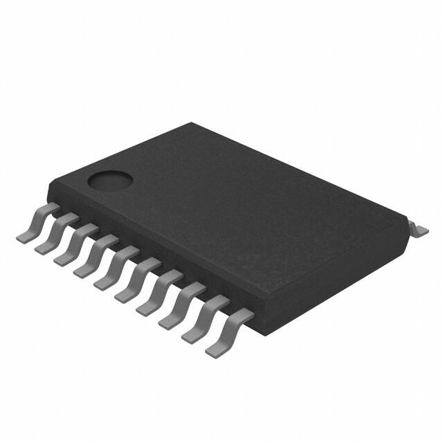
A 20-pin TSSOP package is employed to maximize
board space utilization.
Packaged in 20-pin TSSOP
Available in Pb (lead) free package
Operating voltage of 3.3 V
Low power consumption
Input differential clock of up to 200 MHz (can accept
LVDS, HCSL)
• Outputs, four pairs (HCSL, 0.7 V Current mode
differential pair)
• Jitter 100 ps (peak-to-peak)
• Output skew of 50 ps
• Operating frequency of 80 MHz to 200 MHz
Block Diagram
OE
VDD
2
CLKA
CLKA
IN1
CLKB
IN1
CLKB
MUX
2 to 1
IN2
CLKC
CLKC
IN2
CLKD
CLKD
2
SEL
PD
1
MDS 557-06 B
I n t e gra te d C i r c u i t S y s t e m s
Rr (IREF)
GND
●
525 Race Stre et, San Jo se, CA 9 5126
Revision 021705
●
te l (40 8) 2 97-12 01
●
w w w. i c st . c o m
�ICS557-06
One to Four HCSL Clock Buffer
Pin Assignment
Select table
SEL
1
20
CLKA
VDDIN
2
19
CLKA
SEL
Input Pair
selected
IN1
3
18
CLKB
0
IN2/ IN2
IN1
4
17
CLKB
1
IN1/ IN1
PD
5
16
GND
IN2
6
15
VDD
IN2
7
14
CLKC
OE
8
13
CLKC
GND
9
12
CLKD
IREF
10
11
CLKD
20-pin (173 mil) TSSOP
Pin Descriptions
Pin
Pin
Name
Pin
Type
Pin Description
1
SEL
Input
SEL=1 selects IN1/IN1. SEL =0 selects IN2/ IN2. Internal pull-up resistor.
2
VDDIN
Power
Connect to +3.3 V. Supply voltage for Input clocks.
3
IN1
Input
HCSL/LVDS true input signal 1.
4
IN1
Input
HCSL/LVDS complimentary input signal 1.
5
PD
Input
Powers down the chip and tri-states outputs when low. Internal pull-up resistor.
6
IN2
Input
HCSL/LVDS true input signal 2.
7
IN2
Input
HCSL/LVDS complimentary input signal 2.
8
OE
Input
Provides fast output on, tri-states output (High = enable outputs; Low = disable).
Internal pull-up resistor outputs.
9
GND
Power
Connect to ground.
10
Rr(IREF)
Output
Precision resistor attached to this pin is connected to the internal current reference.
11
CLKD
Output
Differential Complimentary clock.
12
CLKD
Output
Differential True clock.
13
CLKC
Output
Differential Complimentary clock.
14
CLKC
Output
Differential True clock.
15
VDDOUT
Power
Connect to +3.3 V. Supply Voltage for Output Clocks.
16
GND
Power
Connect to ground.
17
CLKB
Output
Differential Complimentary clock.
18
CLKB
Output
Differential True clock.
19
CLKA
Output
Differential Complimentary clock.
20
CLKA
Output
True clock.
2
MDS 557-06 B
In te grated Circuit Systems
●
525 Ra ce Street, San Jose, CA 9512 6
Revision 021705
●
tel (4 08) 297-1 201
●
w w w. i c s t . c o m
�ICS557-06
One to Four HCSL Clock Buffer
Application Information
External Components
Decoupling Capacitors
As with any high-performance mixed-signal IC, the
ICS557-06 must be isolated from system power supply
noise to perform optimally.
Decoupling capacitors of 0.01µF must be connected
between each VDD and the PCB ground plane.
A minimum number of external components are
required for proper operation. Decoupling capacitors of
0.01 µF should be connected between VDD and GND
pairs (2,9 and 15,16) as close to the device as possible.
Current Reference Source Rr (Iref)
PCB Layout Recommendations
If board target trace impedance (Z) is 50Ω, then Rr =
475Ω (1%), providing IREF of 2.32 mA, output current
(IOH) is equal to 6*IREF.
For optimum device performance and lowest output
phase noise, the following guidelines should be
observed.
Each 0.01µF decoupling capacitor should be mounted
on the component side of the board as close to the
VDD pin as possible. No vias should be used between
decoupling capacitor and VDD pin. The PCB trace to
VDD pin should be kept as short as possible, as should
the PCB trace to the ground via. Distance of the ferrite
bead and bulk decoupling from the device is less
critical.
Load Resistors RL
Since the clock outputs are open source outputs, 50
ohm external resistors to ground are to be connected at
each clock output.
2) An optimum layout is one with all components on the
same side of the board, minimizing vias through other
signal layers (the ferrite bead and bulk decoupling
capacitor can be mounted on the back). Other signal
traces should be routed away from the ICS557-06.
This includes signal traces just underneath the device,
or on layers adjacent to the ground plane layer used by
the device.
3
MDS 557-06 B
In te grated Circuit Systems
●
525 Ra ce Street, San Jose, CA 9512 6
Revision 021705
●
tel (4 08) 297-1 201
●
w w w. i c s t . c o m
�ICS557-06
One to Four HCSL Clock Buffer
Absolute Maximum Ratings
Stresses above the ratings listed below can cause permanent damage to the ICS557-06. These ratings are
stress ratings only. Functional operation of the device at these or any other conditions above those
indicated in the operational sections of the specifications is not implied. Exposure to absolute maximum
rating conditions for extended periods can affect product reliability. Electrical parameters are guaranteed
only over the recommended operating temperature range.
Item
Rating
Supply Voltage, VDD, VDDA
5.5 V
All Inputs and Outputs
-0.5 V to VDD+0.5 V
Ambient Operating Temperature
0 to +70°C
Storage Temperature
-65 to +150°C
Junction Temperature
125°C
Soldering Temperature
260°C
ESD Protection (Input)
2000 V min. (HBM)
DC Electrical Characteristics
Unless stated otherwise, VDD = 3.3 V ±5%, Ambient Temperature 0 to +70°C
Parameter
Symbol
Supply Voltage
Conditions
V
1
Min.
Typ.
Max.
3.135
3.465
Units
Input High Voltage
VIH
OE, SEL, PD
2.0
VDD +0.3
V
Input Low Voltage1
VIL
OE, SEL, PD
VSS-0.3
0.8
V
Input Leakage Current2
IIL
0 < Vin < VDD
-5
5
µA
Operating Supply Current
IDD
50Ω, 2pF
55
mA
IDDOE
OE =Low
20
mA
IDDPD
No load, PD =Low
400
µA
Input pin capacitance
7
pF
Output pin capacitance
6
pF
5
nH
Input Capacitance
CIN
Output Capacitance
COUT
Pin Inductance
LPIN
Output Resistance
ROUT
Pull-up Resistor
RPU
CLKOUT
1 Single edge is monotonic when transitioning through
2 Inputs with pull-ups/-downs are not included.
kΩ
110
kΩ
region.
4
MDS 557-06 B
In te grated Circuit Systems
3.0
●
525 Ra ce Street, San Jose, CA 9512 6
Revision 021705
●
tel (4 08) 297-1 201
●
w w w. i c s t . c o m
�ICS557-06
One to Four HCSL Clock Buffer
AC Electrical Characteristics - CLKOUTA/CLKOUTB
Unless stated otherwise, VDD=3.3 V ±5%, Ambient Temperature 0 to +70°C
Parameter
Symbol
Conditions
Min.
Input Frequency
Output Frequency
1,2
Input High Voltage
1,2
Input Low Voltage
Differential Input
Voltages
Input Offset Voltage
Max.
Units
80
200
MHz
80
200
MHz
850
mV
VIH
HCSL
660
VIL
Typ.
700
HCSL
-150
0
(VID)
LVDS
250
350
450
mV
(VIS)
LVDS
1.125
1.25
1.375
V
700
850
mV
550
mV
140
mV
1,2
VOH
HCSL
660
1,2
VOL
Output High Voltage
Output Low Voltage
HCSL
-150
0
Crossing Point
Voltage1,2
Absolute
250
350
Crossing Point
Voltage1,2,4
Variation over all edges
Jitter, Cycle-to-Cycle1,3
mV
mV
100
1,2
ps
Rise Time
tOR
From 0.175 V to 0.525 V
175
332
700
ps
Fall Time1,2
tOF
From 0.525 V to 0.175 V
175
344
700
ps
125
ps
50
ps
Rise/Fall Time
Variation1,2
Skew between Outputs
Measured at crossing point
1,3
Duty Cycle
45
55
%
Output Enable Time5
All outputs
10
us
Output Disable Time5
All outputs
10
us
From power-up VDD=3.3 V
3.0
ms
3.0
ms
3
ns
Stabilization Time
tSTABLE
Spread Change Time
tSPREAD Settling period after spread change
Input to Output Delay
Input differential clock to output
differential clock delay measured at
mid point of input levels to mid pint of
output levels
1
Test setup is RL=50 ohms with 2 pF, Rr = 475Ω (1%).
2
Measurement taken from a single-ended waveform.
3
Measurement taken from a differential waveform.
4
Measured at the crossing point where instantaneous voltages of both CLKOUT and CLKOUT are equal.
5
CLKOUT pins are tri-stated when OE is Low asserted. CLKOUT is driven differential when OE is High unless its
PD = low.
5
MDS 557-06 B
In te grated Circuit Systems
●
525 Ra ce Street, San Jose, CA 9512 6
Revision 021705
●
tel (4 08) 297-1 201
●
w w w. i c s t . c o m
�ICS557-06
One to Four HCSL Clock Buffer
Thermal Characteristics
Parameter
Symbol
Conditions
Min.
Typ.
Max. Units
Thermal Resistance Junction to
Ambient
θJA
Still air
93
°C/W
θJA
1 m/s air flow
78
°C/W
θJA
3 m/s air flow
65
°C/W
Thermal Resistance Junction to Case
θJC
20
°C/W
HCSL Output Loads
6*IREF
IREF
=2.3 mA
RL
50.2 Ω
RL 475 Ω
RL
50.2 Ω
700 mV
0
tOR
500 ps
0.52 V
0.175 V
tOF
0.52 V
0.175 V
6
MDS 557-06 B
In te grated Circuit Systems
500 ps
●
525 Ra ce Street, San Jose, CA 9512 6
Revision 021705
●
tel (4 08) 297-1 201
●
w w w. i c s t . c o m
�ICS557-06
One to Four HCSL Clock Buffer
Marking Diagram
Marking Diagram (Pb free)
20
ICS
11
20
######
YYWW
557G-06
1
11
ICS
10
######
YYWW
557G06LF
1
10
Notes:
1. ###### is the lot code.
2. YYWW is the last two digits of the year, and the week number that the part was assembled.
3. “LF” denotes Pb free package.
4. Bottom marking: (origin). Origin = country of origin if not USA.
7
MDS 557-06 B
In te grated Circuit Systems
●
525 Ra ce Street, San Jose, CA 9512 6
Revision 021705
●
tel (4 08) 297-1 201
●
w w w. i c s t . c o m
�ICS557-06
One to Four HCSL Clock Buffer
Package Outline and Package Dimensions (20-pin TSSOP, 173 Mil. Narrow Body)
Package dimensions are kept current with JEDEC Publication No. 95
Millimeters
20
Symbol
E1
Min
A
A1
A2
b
c
D
E
E1
e
L
α
aaa
E
INDEX
AREA
1 2
D
Inches
Max
1.20
0.05
0.15
0.80
1.05
0.19
0.30
0.09
0.20
6.40
6.60
6.40 BASIC
4.30
4.50
0.65 Basic
0.45
0.75
0°
8°
-0.10
Min
Max
0.047
0.002
0.006
0.032
0.041
0.007
0.012
0.0035 0.008
0.252
0.260
0.252 BASIC
0.169
0.177
0.0256 Basic
0.018
0.030
0°
8°
-0.004
A
A2
A1
c
-Ce
SEATING
PLANE
b
L
aaa C
Ordering Information
Part / Order Number
Marking
Shipping Packaging
Package
Temperature
ICS557G-06
See Page 4
Tubes
20-pin TSSOP
0 to +70° C
ICS557G-06T
Tape and Reel
20-pin TSSOP
0 to +70° C
ICS557G-06LF
Tubes
20-pin TSSOP
0 to +70° C
ICS557G-06LFT
Tape and Reel
20-pin TSSOP
0 to +70° C
While the information presented herein has been checked for both accuracy and reliability, Integrated Circuit Systems (ICS)
assumes no responsibility for either its use or for the infringement of any patents or other rights of third parties, which would
result from its use. No other circuits, patents, or licenses are implied. This product is intended for use in normal commercial
applications. Any other applications such as those requiring extended temperature range, high reliability, or other extraordinary
environmental requirements are not recommended without additional processing by ICS. ICS reserves the right to change any
circuitry or specifications without notice. ICS does not authorize or warrant any ICS product for use in life support devices or
critical medical instruments.
8
MDS 557-06 B
In te grated Circuit Systems
●
525 Ra ce Street, San Jose, CA 9512 6
Revision 021705
●
tel (4 08) 297-1 201
●
w w w. i c s t . c o m
�


 工商网监
湘ICP备2023018690号
工商网监
湘ICP备2023018690号
