DATA SHEET
BIPOLAR ANALOG INTEGRATED CIRCUITS
µPC2757TB, µPC2758TB
UE
D
SILICON MMIC 1st FREQUENCY DOWN-CONVERTER
FOR CELLULAR/CORDLESS TELEPHONE
DESCRIPTION
The µPC2757TB and µPC2758TB are silicon monolithic integrated circuit designed as 1st frequency downconverter for cellular/cordless telephone receiver stage. The ICs consist of mixer and local amplifier. The
µPC2757TB features low current consumption and the µPC2758TB features improved intermodulation. From these
two version, you can chose either IC corresponding to your system design. These TB suffix ICs which are smaller
package than conventional T suffix ICs contribute to reduce your system size.
IN
The µPC2757TB and µPC2758TB are manufactured using Renesas 20 GHz fT NESAT™III silicon bipolar process.
This process uses silicon nitride passivation film and gold electrodes. These materials can protect chip surface from
external pollution and prevent corrosion/migration. Thus, this IC has excellent performance, uniformity and reliability.
FEATURES
: fRFin = 0.1 to 2.0 GHz, fIFout = 20 to 300 MHz
NT
• Wideband operation
• High-density surface mounting
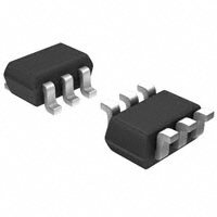
: 6-pin super minimold package
• Low current consumption
: ICC = 5.6 mA TYP. @ µPC2757TB
ICC = 11 mA TYP. @ µPC2758TB
• Supply voltage
: VCC = 2.7 to 3.3 V
• Minimized carrier leakage
: Due to double balanced mixer
• Equable output impedance
: Single-end push-pull IF amplifier
SC
O
• Built-in power save function
APPLICATIONS
• Cellular/cordless telephone up to 2.0 GHz MAX. (example: GSM, PDC800M, PDC1.5G and so on): µPC2758TB
• Cellular/cordless telephone up to 2.0 GHz MAX. (example: CT1, CT2 and so on): µPC2757TB
ORDERING INFORMATION
Part Number
µPC2757TB-E3
6-pin
super
minimold
DI
µPC2758TB-E3
Package
Markings
Supplying Form
C1X
Embossed tape 8 mm wide.
Pin 1, 2, 3 face the tape perforation side.
Qty 3kpcs/reel.
C1Y
Product Type
Low current consumption
High OIP3
Remark To order evaluation samples, please contact your nearby sales office (Part number for sample order:
µPC2757TB-A, µPC2758TB-A).
Document No. P12771EJ3V0DS00 (3rd edition)
Date Published November 2000 N CP(K)
Caution Electro-static sensitive devices
The mark
shows major revised points.
�µPC2757TB, µPC2758TB
CONTENTS
PIN CONNECTIONS............................................................................................................................................. 3
2.
PRODUCT LINE-UP ............................................................................................................................................. 3
3.
INTERNAL BLOCK DIAGRAM ........................................................................................................................... 4
4.
SYSTEM APPLICATION EXAMPLE................................................................................................................... 4
5.
PIN EXPLANATION ............................................................................................................................................. 5
6.
ABSOLUTE MAXIMUM RATINGS...................................................................................................................... 6
7.
RECOMMENDED OPERATING RANGE ............................................................................................................ 6
8.
ELECTRICAL CHARACTERISTICS .................................................................................................................... 6
9.
STANDARD CHARACTERISTICS FOR REFERENCE ..................................................................................... 7
IN
UE
D
1.
NT
10. TEST CIRCUIT ..................................................................................................................................................... 8
11. ILLUSTRATION OF THE TEST CIRCUIT ASSEMBLED ON EVALUATION BOARD ................................. 8
12. TYPICAL CHARACTERISTICS............................................................................................................................ 9
12.1 µPC2757TB.................................................................................................................................................. 9
SC
O
12.2 µPC2758TB................................................................................................................................................ 11
13. S-PARAMETERS ................................................................................................................................................ 13
13.1 µPC2757TB................................................................................................................................................ 13
13.2 µPC2758TB................................................................................................................................................ 14
14. PACKAGE DIMENSIONS .................................................................................................................................... 15
15. NOTE ON CORRECT USE ................................................................................................................................ 16
DI
16. RECOMMENDED SOLDERING CONDITIONS .................................................................................................. 16
2
Data Sheet P12771EJ3V0DS00
�µPC2757TB, µPC2758TB
1. PIN CONNECTIONS
µPC2757TB, µPC2758TB in common
2
1
4
4
3
5
5
2
6
6
1
Pin Name
1
RFinput
2
GND
3
LOinput
4
PS
UE
3
Pin No.
D
(Bottom View)
C1X
(Top View)
Example marking is for µPC2757TB
5
VCC
6
IFoutput
2. PRODUCT LINE-UP (TA = +25°C, VCC = VPS = 3.0 V, ZS = ZL = 50 Ω)
Part No.
No RF
ICC
(mA)
900 MHz 1.5 GHz 1.9 GHz 900 MHz
SSB · NF SSB · NF SSB · NF
CG
(dB)
(dB)
(dB)
(dB)
µPC2757T
µPC2757TB
5.6
10
10
11
9
10
µPC8112T
8.5
µPC8112TB
Items
µPC2757T
900 MHz
PO(sat)
(dBm)
µPC2757TB
−3
µPC2758T
µPC2758TB
µPC8112T
µPC8112TB
Remark
+1
−2.5
900 MHz
IIP3
(dBm)
1.5 GHz
IIP3
(dBm)
1.9 GHz
IIP3
(dBm)
13
15
15
13
−14
−14
−12
13
19
18
17
−13
−12
−11
13
−10
−9
−7
9
11
11
15
13
1.5 GHz
PO(sat)
(dBm)
1.9 GHz
PO(sat)
(dBm)
900 MHz
RFLO
(dB)
1.5 GHz
RFLO
(dB)
1.9 GHz
RFLO
(dB)
−
−
−
SC
O
Part No.
1.9 GHz
CG
(dB)
NT
µPC2758T
µPC2758TB
1.5 GHz
CG
(dB)
IN
Items
−
−
−3
−8
−4
−3
IF Output
Configuration
Packages
6-pin minimold
6-pin super minimold
Emitter follower
−
−
6-pin minimold
−
6-pin super minimold
−80
−57
−55
6-pin minimold
Open collector
6-pin super minimold
Typical performance. Please refer to ELECTRICAL CHARACTERISTICS in detail.
DI
Cautions 1. The µPC2757 and µPC2758’s IIP3 are calculated with ∆IM3 = 3 which is the same IM3
inclination as µPC8112. On the other hand, OIP3 of Standard characteristics in page 7 is
cross point IP.
2. This document is to be specified for µPC2757TB, µPC2758TB.
The other part number
mentioned in this document should be referred to the data sheet of each part number.
Data Sheet P12771EJ3V0DS00
3
�µPC2757TB, µPC2758TB
3. INTERNAL BLOCK DIAGRAM (µPC2757TB, µPC2758TB in common)
IF
output
D
RF
input
LO
input
VCC
GND
4. SYSTEM APPLICATION EXAMPLE
DIGITAL CELLULAR TELEPHONE
DEMOD.
RX
÷N
0˚
TX
PLL
I
φ
PA
DI
SC
O
Driver
4
I
Q
PLL
NT
VCO
SW
IN
µ PC2758TB
Low noise Tr.
UE
POWER
SAVE
Data Sheet P12771EJ3V0DS00
90˚
Q
�µPC2757TB, µPC2758TB
5. PIN EXPLANATION (Both µPC2757TB, 2758TB)
Pin
Name
Applied
Voltage (V)
Pin Voltage
Note
(V)
1
RFinput
−
1.2
–
3
LOinput
–
1.3
PS
VCC or GND
This pin is LO input for local buffer
designed as differential amplifier.
Recommendable input level is –15
to 0 dBm. Also this symmetrical
circuit can keep specified
performance insensitive to processcondition distribution.
–
From
LO
1
−
VCC
Mixer
3
This pin is for power-save function.
This pin can control ON/OFF
operation with bias as follows;
Bias: V
VPS
VCC
4
Operation
≥ 2.5
ON
0 to 0.5
OFF
Rise time/fall time using this pin are
approximately 10 µs.
5
VCC
2.7 to 3.3
–
Supply voltage 3.0 ±0.3 V for
operation. Must be connected
bypass capacitor. (example: 1 000
pF) to minimize ground impedance.
6
IFoutput
–
1.7
This pin is output from IF buffer
amplifier designed as single-ended
push-pull type. This pin is assigned
for emitter follower output with lowimpedance. In the case of
connecting to high-impedance
stage, please attach external
matching circuit.
DI
To IF
Amp.
This pin is ground of IC.
Must be connected to the system
ground with minimum inductance.
Ground pattern on the board should
be formed as wide as possible.
(Track length should be kept as
short as possible.)
SC
O
4
VCC
UE
GND
Internal Equivalent Circuit
IN
GND
This pin is RF input for mixer
designed as double balance type.
This circuit contributes to suppress
spurious signal with minimum LO
and bias power consumption.
Also this symmetrical circuit can
keep specified performance insensitive to process-condition
distribution.
NT
2
Function and Application
D
Pin
No.
−
VCC
6
Note Each pin voltage is measured at VCC = 3.0 V
Data Sheet P12771EJ3V0DS00
5
�µPC2757TB, µPC2758TB
6. ABSOLUTE MAXIMUM RATINGS
Parameter
Symbol
Conditions
Ratings
Unit
VCC
TA = +25°C
5.5
V
Power Dissipation of Package Allowance
PD
Mounted on 50 × 50 × 1.6 mm
double sided copper clad epoxy
glass board at TA = +85°C
270
mW
Operating Ambient Temperature
TA
Storage Temperature
Tstg
PS Pin Voltage
VPS
7. RECOMMENDED OPERATING RANGE
Symbol
MIN.
TYP.
MAX.
Supply Voltage
VCC
2.7
3.0
3.3
Operating Ambient Temperature
TA
–40
PLOin
–15
LO Input Power
°C
–55 to +150
°C
5.5
V
Unit
V
IN
Parameter
–40 to +85
UE
TA = +25°C
D
Supply Voltage
+25
+85
°C
–10
0
dBm
NT
8. ELECTRICAL CHARACTERISTICS (TA = +25°C, VCC = VPS = 3.0 V, PLOin = –10 dBm,
ZS = ZL = 50 Ω)
µPC2757TB
Parameter
Symbol
ICC
RF Input Frequency
fRFin
TYP.
MAX.
MIN.
TYP.
MAX.
No input signal
3.7
5.6
7.7
6.6
11
14.8
mA
CG ≥ (CG1 –3 dB)
fIFout = 130 MHz constant
0.1
−
2.0
0.1
−
2.0
GHz
IF Output Frequency
fIFout
CG ≥ (CG1 –3 dB)
fRFin = 0.8 GHz constant
20
−
300
20
−
300
MHz
Conversion Gain 1
CG1
fRFin = 0.8 GHz, fIFout = 130 MHz
PRFin = –40 dBm, Upper local
12
15
18
16
19
22
dB
Conversion Gain 2
CG2
fRFin = 2.0 GHz, fIFout = 250 MHz
PRFin = –40 dBm, Lower local
10
13
16
14
17
20
dB
SSB Noise Figure 1
SSB • NF1 fRFin = 0.8 GHz, fIFout = 130 MHz,
SSB mode, Upper local
−
10
13
−
9
12
dB
SSB Noise Figure 2
SSB • NF2 fRFin = 2.0 GHz, fIFout = 250 MHz,
SSB mode, Lower local
−
13
16
−
13
15
dB
fRFin = 0.8 GHz, fIFout = 130 MHz
PRFin = –10 dBm, Upper local
–11
–3
−
–7
+1
−
dBm
fRFin = 2.0 GHz, fIFout = 250 MHz
PRFin = –10 dBm, Lower local
–11
–8
−
–7
–4
−
dBm
Saturated Output
Power 1
PO(sat) 1
Saturated Output
Power 2
PO(sat) 2
DI
6
Unit
MIN.
SC
O
Circuit Current
µPC2758TB
Conditions
Data Sheet P12771EJ3V0DS00
�µPC2757TB, µPC2758TB
9. STANDARD CHARACTERISTICS FOR REFERENCE
(Unless otherwise specified: TA = +25°C, VCC = VPS = 3.0 V, PLOin = –10 dBm, ZS = ZL = 50 Ω)
Reference Value
Conditions
3rd Order Distortion Output
Intercept Point
OIP3
fRFin = 0.8 to 2.0 GHz, fIFout = 0.1 GHz,
Cross point IP
LO Leakage at RF pin
LOrf
LO Leakage at IF pin
LOif
ICC(PS)
µPC2758TB
Unit
+5
+11
dBm
fLOin = 0.8 to 2.0 GHz
–35
–30
dBm
fLOin = 0.8 to 2.0 GHz
–23
–15
dBm
0.1
0.1
µA
VPS = 0.5 V
DI
SC
O
NT
IN
Circuit Current at Power Save
Mode
µPC2757TB
D
Symbol
UE
Parameter
Data Sheet P12771EJ3V0DS00
7
�µPC2757TB, µPC2758TB
10. TEST CIRCUIT
µPC2757TB, µPC2758TB
(Top View)
POWER
SAVE
1 000 pF
50 Ω
3
LOinput
PS
4
2
GND
VCC
3 300 pF
5
3V
C3
1
RFinput IFoutput
1 000 pF
C1
6
UE
C2
Signal Generator
50 Ω
D
Signal Generator
3 300 pF
C4
50 Ω
Spectrum Analyzer
IN
11. ILLUSTRATION OF THE TEST CIRCUIT ASSEMBLED ON EVALUATION BOARD
C2
VCC
SC
O
GND
NT
C3
LO
input
RF
input
C1
Component List
2. Back side: GND pattern
C1, C2
1 000 pF
3. Solder plated on pattern
C3 to C5
3 300 pF
4. °{: Through holes
DI
PS
C4
→
Voltage supply
C5
IF
output
Notes 1. 35 × 42 × 0.4 mm double sided copper clad polyimide board.
Value
No.
PS bias
Application explanation
This IC is guaranteed on the test circuit constructed with 50 Ω equipment and transmission line.
This IC, however, does not have 50 Ω input/output impedance, but electrical characteristics such as conversion
gain and intermodulation distortion are described herein on these conditions without impedance matching. So, you
should understand that conversion gain and intermodulation distortion at input level will vary when you improve VS of
RF input with external circuit (50 Ω termination or impedance matching.)
8
Data Sheet P12771EJ3V0DS00
�µPC2757TB, µPC2758TB
12. TYPICAL CHARACTERISTICS (TA = +25°°C, on Measurement Circuit)
12.1 µPC2757TB
CIRCUIT CURRENT vs. SUPPLY VOLTAGE
CONVERSION GAIN vs. RF INPUT FREQUENCY
7
6
5
4
3
2
1
1
2
3
4
Supply Voltage VCC (V)
5
6
SSB NOISE FIGURE vs. RF INPUT FREQUENCY
12
10
VCC = VPS = 3.0 V
PRFin = –40 dBm
8 PLOin = –10 dBm
fIFout = 130 MHz
6
0
0.5
1.0
1.5
2.0
RF Input Frequency fRFin (GHz)
20
14
13
12
11
10
9
VCC = VPS = 3.0 V
PRFin = –40 dBm
PLOin = –10 dBm
fIFout = 130 MHz
8
7
18
16
SC
O
1.6
1.8
2.0
2.2
2.4
RF Input Frequency fRFin (GHz)
12
10
8
6
2.6
20
10
DI
5
VCC = VPS = 3.0 V
fRFin = 900 MHz
fLOin = 800 MHz
PRFin = –40 dBm
–40
–30
–20
–10
0
LO Input Power PLOin (dBm)
10
Conversion Gain CG (dB)
20
15
0
100 200 300 400 500 600
IF Output Frequency fIFout (MHz)
700
CONVERSION GAIN vs. LO INPUT POWER
25
–5
–50
VCC = VPS = 3.0 V
PRFin = –40 dBm
PLOin = –10 dBm
fRFin = 800 MHz
14
25
0
2.5
CONVERSION GAIN vs. IF OUTPUT FREQUENCY
CONVERSION GAIN vs. LO INPUT POWER
Conversion Gain CG (dB)
14
NT
SSB Noise Figure SSB • NF (dB)
15
6
1.4
16
IN
0
Conversion Gain CG (dB)
0
18
UE
Conversion Gain CG (dB)
Circuit Current ICC (mA)
No input signal
8 VCC = VPS
D
20
9
15
10
5
0
–5
–50
Data Sheet P12771EJ3V0DS00
VCC = VPS = 3.0 V
fRFin = 2.0 GHz
fLOin = 1.9 GHz
PRFin = –40 dBm
–40
–30
–20
–10
0
LO Input Power PLOin (dBm)
10
9
�fRFin = 800 MHz
10 fLOin = 930 MHz
PLOin = –10 dBm
0
VCC = VPS = 3.0 V
–10
–20
Pout
–30
–40
IM3
–50
–60
–70
–50 –45 –40 –35 –30 –25 –20 –15 –10 –5
RF Input Power PRFin (dBm)
–30
–45
–50
–55
0
–50
–60
IM3
–70
–50 –45 –40 –35 –30 –25 –20 –15 –10 –5
RF Input Power PRFin (dBm)
PLOin = –10 dBm
V
–15 CC = VPS = 3.0 V
–20
–25
0.5
1
1.5
2
LO Input Frequency fLOin (GHz)
2.5
–30
–35
–40
–45
0
SC
O
–60
–40
LO LEAKAGE AT IF PIN vs.
LO INPUT FREQUENCY
LO Leakage at IF Pin LOif (dBm)
–25
–40
Pout
–30
–10
PLOin = –10 dBm
–15 VCC = VPS = 3.0 V
–20
–35
–20
NT
LO Leakage at RF Pin LOrf (dBm)
–10
fRFin = 2 GHz
10 fLOin = 1.75 GHz
PLOin = –10 dBm
0
VCC = VPS = 3.0 V
–10
IN
LO LEAKAGE AT RF PIN vs.
LO INPUT FREQUENCY
20
DI
Remark The graphs indicate nominal characteristics.
10
D
20
IF OUTPUT POWER OF EACH TONE,
IM3 vs. RF INPUT POWER
UE
IF OUTPUT POWER OF EACH TONE,
IM3 vs. RF INPUT POWER
IF Output Power of Each Tone PIFout(each) (dBm)
3rd Order Intemodulation Distortion IM3 (dBm)
IF Output Power of Each Tone PIFout(each) (dBm)
3rd Order Intemodulation Distortion IM3 (dBm)
µPC2757TB, µPC2758TB
Data Sheet P12771EJ3V0DS00
0.5
1
1.5
2
LO Input Frequency fLOin (GHz)
2.5
�µPC2757TB, µPC2758TB
12.2 µPC2758TB
10
5
0
1
2
3
4
Supply Voltage VCC (V)
5
14
12
0
CONVERSION GAIN vs. IF OUTPUT FREQUENCY
IN
Conversion Gain CG (dB)
18
17
16
15
14
13
12
11
10
3.0
SC
O
0.5
1.0
1.5
2.0
2.5
RF Input Frequency fRFin (GHz)
CONVERSION GAIN vs. LO INPUT POWER
20
20
10
5
VCC = VPS = 3.0 V
fRFin = 800 MHz
fLOin = 930 MHz
PRFin = –40 dBm
DI
–5
–50
–40
–30
–20
–10
0
LO Input Power PLOin (dBm)
10
Conversion Gain CG (dB)
25
15
0
VCC = VPS = 3.0 V
PRFin = –40 dBm
PLOin = –10 dBm
fRFin = 800 MHz
100
200
300
400
500
IF Output Frequency fIFout (MHz)
600
CONVERSION GAIN vs. LO INPUT POWER
25
0
3.0
19
15
10
0.5
1.0
1.5
2.0
2.5
RF Input Frequency fRFin (GHz)
20
VCC = VPS = 3.0 V
PRFin = –40 dBm
PLOin = –10 dBm
fIFout = 130 MHz
5
0.0
Conversion Gain CG (dB)
16
NT
SSB Noise Figure SSB • NF (dB)
20
18
10
6
SSB NOISE FIGURE vs. RF INPUT FREQUENCY
24 VCC = VPS = 3.0 V
PRFin = –40 dBm
22 PLOin = –10 dBm
fIFout = 130 MHz
20
D
Conversion Gain CG (dB)
Circuit Current ICC (mA)
No input signal
VCC = VPS
15
0
CONVERSION GAIN vs. RF INPUT FREQUENCY
UE
CIRCUIT CURRENT vs. SUPPLY VOLTAGE
20
15
10
5
0
–5
–50
Data Sheet P12771EJ3V0DS00
VCC = VPS = 3.0 V
fRFin = 2.0 GHz
fLOin = 1.9 GHz
PRFin = –40 dBm
–40
–30
–20
–10
0
LO Input Power PLOin (dBm)
10
11
�0
–10
–20
–30
–40
fRF1 = 800 MHz
fRF2 = 805 MHz
fLO = 900 MHz
PLOin = –10 dBm
VCC = VPS = 3.0 V
–60
–70
–80
–50
–40
–30
–20
–10
0
RF Input Power PRFin (dBm)
LO LEAKAGE AT RF PIN vs.
LO INPUT FREQUENCY
–10
–20
–30
–40
–50
–60
–70
–80
–50
–40
–30
–20
–10
0
RF Input Power PRFin (dBm)
10
LO LEAKAGE AT IF PIN vs.
LO INPUT FREQUENCY
–20
–30
–40
–50
PLOin = –10 dBm
VCC = VPS = 3.0 V
–20
0.5
1.0
1.5
2.0
2.5
LO Input Frequency fLOin (GHz)
3.0
–30
–40
–50
–60
0
SC
O
0
–10
DI
Remark The graphs indicate nominal characteristics.
12
fRF1 = 2.0 GHz
fRF2 = 2.005 GHz
fLO = 1.9 GHz
PLOin = –10 dBm
VCC = VPS = 3.0 V
0
–10
–60
0
NT
LO Leakage at RF Pin LOrf (dBm)
0
10
10
IN
–50
20
D
10
IF OUTPUT POWER OF EACH TONE,
IM3 vs. RF INPUT POWER
UE
20
IF Output Power of Each Tone PIFout(each) (dBm)
3rd Order Intermodulation Distortion IM3 (dBm)
IF OUTPUT POWER OF EACH TONE,
IM3 vs. RF INPUT POWER
LO Leakage at IF Pin LOif (dBm)
IF Output Power of Each Tone PIFout(each) (dBm)
3rd Order Intermodulation Distortion IM3 (dBm)
µPC2757TB, µPC2758TB
Data Sheet P12771EJ3V0DS00
PLOin = –10 dBm
VCC = VPS = 3.0 V
0.5
1.0
1.5
2.0
2.5
LO Input Frequency fLOin (GHz)
3.0
�µPC2757TB, µPC2758TB
13. S-PARAMETERS
13.1 µPC2757TB
D
Calibrated on pin of DUT
S11
Z
REF 1.0 Units
1
200.0 mUnits/
104.03 Ω –413.42 Ω
hp
MARKER 1
500.0 MHz
1
2
4
3
RF PORT
VCC = 3.0V VPS = GND
1:500 MHz 104.03 Ω -j413.42 Ω
2:900 MHz 74.82 Ω -j243.06 Ω
3:1 500 MHz 59.266 Ω -j154.98 Ω
4:1 900 MHz 51.227 Ω -j124.55 Ω
5:2 500 MHz 43.996 Ω -j95.117 Ω
IN
5
RF PORT
VCC = VPS = 3.0V
1:500 MHz 56.422 Ω -j275.59 Ω
2:900 MHz 38.68 Ω -j152.71 Ω
3:1 500 MHz 31.699 Ω -j88.102 Ω
4:1 900 MHz 29.209 Ω -j65.926 Ω
5:2 500 MHz 29.209 Ω -j44.758 Ω
UE
S11
Z
REF 1.0 Units
1
200.0 mUnits/
56.422 Ω –275.59 Ω
hp
MARKER 1
500.0 MHz
START 0.050000000 GHz
STOP 3.000000000 GHz
2
5
4
3
START 0.050000000 GHz
STOP 3.000000000 GHz
S11
Z
REF 1.0 Units
1
200.0 mUnits/
114.16 Ω –400.03 Ω
hp
MARKER 1
500.0 MHz
NT
S11
Z
REF 1.0 Units
1
200.0 mUnits/
90.969 Ω –243.41 Ω
hp
MARKER 1
500.0 MHz
1
1
SC
O
1
5
LO PORT
VCC = VPS = 3.0V
1:500 MHz 90.969 Ω -j243.41 Ω
2:900 MHz 67.828 Ω -j150.32 Ω
3:1 500 MHz 51.488 Ω -j97.273 Ω
4:1 900 MHz 44.621 Ω -j77.352 Ω
5:2 500 MHz 39.627 Ω -j56.738 Ω
2
2
4 3
START 0.050000000 GHz
STOP 3.000000000 GHz
S22
Z
REF 1.0 Units
1
200.0 mUnits/
19.146 Ω 7.2041 Ω
hp
MARKER 1
130.0 MHz
5
LO PORT
VCC = 3.0V VPS = GND
1:500 MHz 114.16 Ω -j400.03 Ω
2:900 MHz 75.133 Ω -j242.73 Ω
3:1 500 MHz 53.516 Ω -j154.21 Ω
4:1 900 MHz 44.789 Ω -j124.74 Ω
5:2 500 MHz 37.004 Ω -j93.828 Ω
4
3
START 0.050000000 GHz
STOP 3.000000000 GHz
S22
Z
REF 1.0 Units
1
200.0 mUnits/
066.38 Ω –1.3174 kΩ
hp
MARKER 1
130.0 MHz
DI
1
IF PORT
VCC = VPS = 3.0V
1:130 MHz 19.146 Ω -j7.2041 Ω
2:250 MHz 22.73 Ω -j12.909 Ω
2
1
2
START 0.050000000 GHz
STOP 3.000000000 GHz
IF PORT
VCC = 3.0V VPS = GND
1:130 MHz 66.38 Ω -j1.3174 kΩ
2:250 MHz 88.281 Ω -j725.41 Ω
Data Sheet P12771EJ3V0DS00
START 0.050000000 GHz
STOP 3.000000000 GHz
13
�µPC2757TB, µPC2758TB
13.2 µPC2758TB
S11
Z
REF 1.0 Units
1
200.0 mUnits/
63.312 Ω –261.34 Ω
hp
MARKER 1
500.0 MHz
S11
Z
REF 1.0 Units
1
200.0 mUnits/
107.13 Ω –395.56 Ω
hp
MARKER 1
500.0 MHz
D
Calibrated on pin of DUT
UE
1
1
2
5
4
5
3
RF PORT
VCC = 3.0V VPS = GND
1:500 MHz 107.13 Ω -j395.56 Ω
2:900 MHz 78.711 Ω -j234.41 Ω
3:1 500 MHz 61.922 Ω -j148.82 Ω
4:1 900 MHz 52.629 Ω -j119.55 Ω
5:2 500 MHz 44.766 Ω -j90.578 Ω
START 0.050000000 GHz
STOP 3.000000000 GHz
4
3
START 0.050000000 GHz
STOP 3.000000000 GHz
IN
RF PORT
VCC = VPS = 3.0V
1:500 MHz 63.312 Ω -j261.34 Ω
2:900 MHz 40.227 Ω -j142.36 Ω
3:1 500 MHz 32.441 Ω -j79.68 Ω
4:1 900 MHz 31.107 Ω -j58.273 Ω
5:2 500 MHz 30.871 Ω -j39.08 Ω
2
Z
S11
REF 1.0 Units
1
200.0 mUnits/
100.31 Ω –374.75 Ω
hp
MARKER 1
500.0 MHz
NT
Z
S11
REF 1.0 Units
1
200.0 mUnits/
73.398 Ω –188.13 Ω
hp
MARKER 1
500.0 MHz
1
1
5
2
2
START 0.050000000 GHz
STOP 3.000000000 GHz
SC
O
LO PORT
VCC = VPS = 3.0V
1:500 MHz 73.398 Ω -j188.13 Ω
2:900 MHz 64.551 Ω -j112.66 Ω
3:1 500 MHz 53.133 Ω -j72.941 Ω
4:1 900 MHz 48.111 Ω -j57.307 Ω
5:2 500 MHz 44.541 Ω -j41.564 Ω
4 3
S22
Z
REF 1.0 Units
1
200.0 mUnits/
15.696 Ω 9.5011 Ω
hp
MARKER 1
130.0 MHz
LO PORT
VCC = 3.0V VPS = GND
1:500 MHz 100.31 Ω -j374.75 Ω
2:900 MHz 73.148 Ω -j223.07 Ω
3:1 500 MHz 57.719 Ω -j144.02 Ω
4:1 900 MHz 50.738 Ω -j119.52 Ω
5:2 500 MHz 41.836 Ω -j90.25 Ω
5
4
3
START 0.050000000 GHz
STOP 3.000000000 GHz
S22
Z
REF 1.0 Units
1
200.0 mUnits/
106.69 Ω –1.3425 kΩ
hp
MARKER 1
130.0 MHz
1
DI
2
IF PORT
VCC = VPS = 3.0V
1:130 MHz 15.696 Ω -j9.5811 Ω
2:250 MHz 21.4 Ω -j16.331 Ω
14
START 0.050000000 GHz
STOP 3.000000000 GHz
1
2
IF PORT
VCC = 3.0V VPS = GND
1:130 MHz 106.69 Ω -j1.3425 kΩ
2:250 MHz 83.75 Ω -j711.47 Ω
Data Sheet P12771EJ3V0DS00
START 0.050000000 GHz
STOP 3.000000000 GHz
�µPC2757TB, µPC2758TB
14. PACKAGE DIMENSIONS
6-PIN SUPER MINIMOLD (UNIT: mm)
0.2+0.1
–0.05
UE
0.65
0.65
1.3
2.0±0.2
1.25±0.1
D
2.1±0.1
0.15+0.1
–0.05
IN
DI
SC
O
NT
0 to 0.1
0.7
0.9±0.1
0.1 MIN.
Data Sheet P12771EJ3V0DS00
15
�µPC2757TB, µPC2758TB
15. NOTE ON CORRECT USE
(1) Observe precautions for handling because of electrostatic sensitive devices.
(2) Form a ground pattern as widely as possible to minimize ground impedance (to prevent undesired oscillation).
(4) The DC cut capacitor must be attached to input pin.
16. RECOMMENDED SOLDERING CONDITIONS
Soldering Method
Soldering Condition
Package peak temperature: 235°C or below
Time: 30 seconds or less (at 210°C)
Note
Count: 3, Exposure limit: None
VPS
Package peak temperature: 215°C or below
Time: 40 seconds or less (at 200°C)
Note
Count: 3, Exposure limit: None
Wave Soldering
Soldering bath temperature: 260°C or below
Time: 10 seconds or less
Note
Count: 1, Exposure limit: None
Partial Heating
Pin temperature: 300°C
Time: 3 seconds or less (per side of device)
Note
Exposure limit: None
Recommended Condition Symbol
NT
IN
Infrared Reflow
UE
This product should be soldered under the following recommended conditions.
D
Keep the track length of the ground pins as short as possible.
(3) Connect a bypass capacitor (example: 1 000 pF) to the VCC pin.
IR35-00-3
VP15-00-3
WS60-00-1
–
Note After opening the dry pack, keep it in a place below 25°C and 65% RH for the allowable storage period.
SC
O
Caution Do not use different soldering methods together (except for partial heating).
For details of recommended soldering conditions for surface mounting, refer to information document
DI
SEMICONDUCTOR DEVICE MOUNTING TECHNOLOGY MANUAL (C10535E).
16
Data Sheet P12771EJ3V0DS00
�NOTICE
Descriptions of circuits, software and other related information in this document are provided only to illustrate the operation of semiconductor products and
application examples. You are fully responsible for the incorporation of these circuits, software, and information in the design of your equipment. California
Eastern Laboratories and Renesas Electronics assumes no responsibility for any losses incurred by you or third parties arising from the use of these circuits,
software, or information.
2.
California Eastern Laboratories has used reasonable care in preparing the information included in this document, but California Eastern Laboratories does
not warrant that such information is error free. California Eastern Laboratories and Renesas Electronics assumes no liability whatsoever for any damages
incurred by you resulting from errors in or omissions from the information included herein.
3.
California Eastern Laboratories and Renesas Electronics do not assume any liability for infringement of patents, copyrights, or other intellectual property
rights of third parties by or arising from the use of Renesas Electronics products or technical information described in this document. No license, express,
implied or otherwise, is granted hereby under any patents, copyrights or other intellectual property rights of California Eastern Laboratories or Renesas
Electronics or others.
4.
You should not alter, modify, copy, or otherwise misappropriate any Renesas Electronics product, whether in whole or in part. California Eastern
Laboratories and Renesas Electronics assume no responsibility for any losses incurred by you or third parties arising from such alteration, modification, copy
or otherwise misappropriation of Renesas Electronics product.
5.
Renesas Electronics products are classified according to the following two quality grades: “Standard” and “High Quality”. The recommended applications
for each Renesas Electronics product depends on the product’s quality grade, as indicated below. “Standard”: Computers; office equipment; communications
equipment; test and measurement equipment; audio and visual equipment; home electronic appliances; machine tools; personal electronic equipment; and
industrial robots etc. “High Quality”: Transportation equipment (automobiles, trains, ships, etc.); traffic control systems; anti-disaster systems; anti-crime
systems; and safety equipment etc. Renesas Electronics products are neither intended nor authorized for use in products or systems that may pose a direct
threat to human life or bodily injury (artificial life support devices or systems, surgical implantations etc.), or may cause serious property damages (nuclear
reactor control systems, military equipment etc.). You must check the quality grade of each Renesas Electronics product before using it in a particular
application. You may not use any Renesas Electronics product for any application for which it is not intended. California Eastern Laboratories and Renesas
Electronics shall not be in any way liable for any damages or losses incurred by you or third parties arising from the use of any Renesas Electronics product
for which the product is not intended by California Eastern Laboratories or Renesas Electronics.
6.
You should use the Renesas Electronics products described in this document within the range specified by California Eastern Laboratories, especially with
respect to the maximum rating, operating supply voltage range, movement power voltage range, heat radiation characteristics, installation and other product
characteristics. California Eastern Laboratories shall have no liability for malfunctions or damages arising out of the use of Renesas Electronics products
beyond such specified ranges.
7.
Although Renesas Electronics endeavors to improve the quality and reliability of its products, semiconductor products have specific characteristics such as
the occurrence of failure at a certain rate and malfunctions under certain use conditions. Further, Renesas Electronics products are not subject to radiation
resistance design. Please be sure to implement safety measures to guard them against the possibility of physical injury, and injury or damage caused by
fire in the event of the failure of a Renesas Electronics product, such as safety design for hardware and software including but not limited to redundancy,
fire control and malfunction prevention, appropriate treatment for aging degradation or any other appropriate measures. Because the evaluation of
microcomputer software alone is very difficult, please evaluate the safety of the final products or systems manufactured by you.
8.
Please contact a California Eastern Laboratories sales office for details as to environmental matters such as the environmental compatibility of each Renesas
Electronics product. Please use Renesas Electronics products in compliance with all applicable laws and regulations that regulate the inclusion or use of
controlled substances, including without limitation, the EU RoHS Directive. California Eastern Laboratories and Renesas Electronics assume no liability for
damages or losses occurring as a result of your noncompliance with applicable laws and regulations.
9.
Renesas Electronics products and technology may not be used for or incorporated into any products or systems whose manufacture, use, or sale is prohibited
under any applicable domestic or foreign laws or regulations. You should not use Renesas Electronics products or technology described in this document
for any purpose relating to military applications or use by the military, including but not limited to the development of weapons of mass destruction. When
exporting the Renesas Electronics products or technology described in this document, you should comply with the applicable export control laws and
regulations and follow the procedures required by such laws and regulations.
10. It is the responsibility of the buyer or distributor of California Eastern Laboratories, who distributes, disposes of, or otherwise places the Renesas Electronics
product with a third party, to notify such third party in advance of the contents and conditions set forth in this document, California Eastern Laboratories and
Renesas Electronics assume no responsibility for any losses incurred by you or third parties as a result of unauthorized use of Renesas Electronics products.
11. This document may not be reproduced or duplicated in any form, in whole or in part, without prior written consent of California Eastern Laboratories.
12. Please contact a California Eastern Laboratories sales office if you have any questions regarding the information contained in this document or Renesas
Electronics products, or if you have any other inquiries.
SC
O
NT
IN
UE
D
1.
NOTE 1: “Renesas Electronics” as used in this document means Renesas Electronics Corporation and also includes its majority-owned subsidiaries.
NOTE 2: “Renesas Electronics product(s)” means any product developed or manufactured by or for Renesas Electronics.
NOTE 3: Products and product information are subject to change without notice.
DI
CEL Headquarters • 4590 Patrick Henry Drive, Santa Clara, CA 95054 • Phone (408) 919-2500 • www.cel.com
For a complete list of sales offices, representatives and distributors,
Please visit our website: www.cel.com/contactus
�


 工商网监
湘ICP备2023018690号
工商网监
湘ICP备2023018690号
