Rcaflga_j�Lmrc
R
caflga_j�L
Single-chip Type with built-in FET Switching Regulator Series
Flexible Step-down
Switching Regulators
with Built-in Power MOSFET
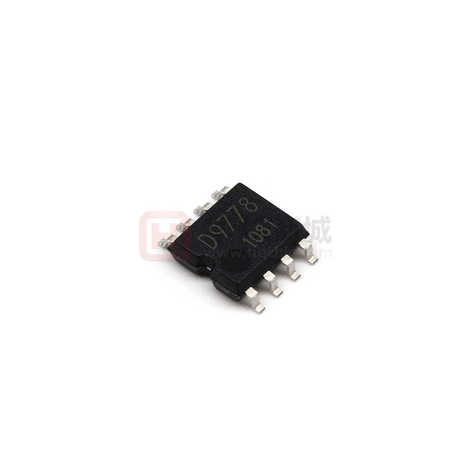
BD9778F, BD9778HFP, BD9001F, BD9781HFP
No.10027EBT41
Overview
The flexible step-down switching regulator controller is a switching regulator controller designed with a high-withstand-voltage
built-in POWER MOS FET, providing a free setting function of operating frequency with external resistor. This switching regulator
controller features a wide input voltage range (7 V to 35 V or 7 V to 48 V) and operating temperature range (-40˚C to +125˚C or
-40˚C to +95˚C). Furthermore, an external synchronization input pin (BD9781HFP) enables synchronous operation with external
clock.
Features
1)
2)
3)
4)
5)
6)
8)
9)
10)
11)
12)
13)
14)
15)
Minimal external components
Wide input voltage range: 7 V to 35 V (BD9778F/HFP and BD9781HFP), 7 V to 48 V (BD9001F)
Built-in P-ch POWER MOS FET
Output voltage setting enabled with external resistor: 1 to VIN
Reference voltage accuracy: ±2%
Wide operating temperature range: -40˚C to +125˚C (BD9778F/HFP and BD9781HFP),
-40˚C to +95˚C (BD9001F)
Low dropout: 100% ON Duty cycle
Standby mode supply current: 0 µA (Typ.) (BD9778F/HFP and BD9781HFP), 4 µA (Typ.) (BD9001F)
Oscillation frequency variable with external resistor: 50 to 300 kHz (BD9001F),
50 to 500 kHz (BD9778F/HFP and BD9781HFP)
External synchronization enabled (only on the BD9781HFP)
Soft start function : soft start time fixed to 5 ms (Typ.))
Built-in overcurrent protection circuit
Built-in thermal shutdown protection circuit
High power HRP7 package mounted (BD9778HFP and BD9781HFP)
Compact SOP8 package mounted (BD9778F and BD9001F)
Applications
All fields of industrial equipment, such as Flat TV , printer, DVD, car audio, car navigation,
and communication such as ETC, AV, and OA.
Product lineup
Item
Output current
Input range
Oscillation frequency range
External synchronization
Standby function
Operating temperature
Package
BD9778F/HFP
2A
7V ~ 35V
50 ~ 500kHz
Not provided
Provided
-40˚C ~ +125˚C
SOP8 / HRP7
www.rohm.com
© 2010 ROHM Co., Ltd. All rights reserved.
BD9001F
2A
7V ~ 48V
50 ~ 300kHz
Not provided
Provided
-40˚C ~ +95˚C
SOP8
1/16
BD9781HFP
4A
7V ~ 35V
50 ~ 500kHz
Provided
Provided
-40˚C ~ +125˚C
HRP7
Dec.2015 - Rev.C
�Technical Note
BD9778F, BD9778HFP, BD9001F, BD9781HFP
Absolute Maximum Ratings(Ta = 25˚C)
Parameter
BD9778F/HFP,BD9781HFP
Power supply
BD9001F
voltage
Output switch pin voltage
Output switch current
Limits
36
50
VIN
2
4
VIN
7
5.5
0.69
-40 ~ +125
-40 ~ +95
-55 ~ +150
150
VIN
VSW
BD9778F/HFP, BD9001F
BD9781HFP
ISW
VEN/SYNC,VEN
VRT,VFB,VINV
EN/SYNC, EN pin voltage
RT, FB, INV pin voltage
Power dissipation
Symbol
HRP7
Pd
SOP8
Operating temperature BD9778F/HFP,BD9781HFP
range
BD9001F
Storage temperature range
Maximum junction temperature
Topr
Tstg
Tjmax
Unit
V
V
*1
*1
A
V
*2
*3
W
˚C
˚C
˚C
*1 Should not exceed Pd-value.
*2 Reduce by 44mW/°C over 25°C, when mounted on 2-layer PCB of 70 X 70 X 1.6 mm3.
(PCB incorporates thermal via. Copper foil area on the front side of PCB: 10.5 X 10.5 mm2. Copper foil area on the reverse side of PCB: 70 X 70 mm2)
*3 Reduce by 5.52 mW/°C over 25°C, when mounted on 2-layer PCB of 70 X 70 X 1.6 mm3.
Recommended operating range
Parameter
Operating power supply voltage
Output switch current
Output voltage (ON Duty)
Oscillation frequency
Oscillation frequency set resistance
BD9778F/HFP
7 ~ 35
~2
6 ~ 100
50 ~ 500
40 ~ 800
BD9001F
7 ~ 48
~2
6 ~ 100
50 ~ 300
100 ~ 800
BD9781HFP
7 ~ 35
~4
6 ~ 100
50 ~ 500
39 ~ 800
Unit
V
A
%
kHz
kΩ
BD9778F/HFP
5 ~ 35
BD9001F
7 ~ 48
BD9781HFP
5 ~ 35
Unit
V
Possible operating range
Parameter
Operating power supply voltage
Electrical characteristics
BD9778F/HFP (Unless otherwise specified, Ta = -40˚C to +125˚C, VIN =13.2 V, VEN = 5 V)
Parameter
Symbol
ISTB
Standby circuit current
IQ
Circuit current
[SW block]
RON
POWER MOS FET ON resistance
IOLIMIT
Operating output current of overcurrent protection
IOLEAK
Output leak current
[Error Amp block]
VREF1
Reference voltage 1
VREF2
Reference voltage 2
∆VREF
Reference voltage input regulation
IB
Input bias current
VFBH
Maximum FB voltage
VFBL
Minimum FB voltage
IFBSINK
FB sink current
IFBSOURCE
FB source current
TSS
Soft start time
[Oscillator block]
FOSC
Oscillation frequency
∆FOSC
Frequency input regulation
[Enable block]
VEN
Threshold voltage
IEN
Sink current
Min.
-
Limits
Typ. Max.
0
10
3
4.2
Unit
Condition
µA
mA
VEN=0V,Ta=25˚C
IO=0A
2
-
0.53
4
0
0.9
30
Ω
A
µA
ISW=50mA
* Design assurance
VIN=35V,VEN=0V
0.98
0.96
-1
2.4
-5.0
70
-
1.00
1.00
0.5
2.5
0.05
-3.0
120
5
1.02
1.04
0.10
-0.5
170
-
V
V
%
µA
V
V
mA
µA
mS
VFB=VINV,Ta=25˚C
VFB=VINV
VIN=5 ~ 35V
VINV=1.1V
VINV=0.5V
VINV=1.5V
VFB=1.5V,VINV=1.5V
VFB=1.5V,VINV=0.5V
* Design assurance
82
-
102
1
122
-
kHz
%
RT=390kΩ
VIN=5 ~ 35V
0.8
-
1.7
13
2.6
50
V
µA
VEN=5V
* Not designed to be radiation-resistant.
www.rohm.com
© 2010 ROHM Co., Ltd. All rights reserved.
2/16
Dec.2015 - Rev.C
�Technical Note
BD9778F, BD9778HFP, BD9001F, BD9781HFP
BD9001F (Unless otherwise specified, Ta=-40˚C ~ +95˚C,VIN=13.2V, VEN=5V)
Parameter
Symbol
Standby circuit current
ISTB
IQ
Circuit current
[SW block]
RON
POWER MOS FET ON resistance
IOLIMIT
Operating output current of overcurrent protection
[Error Amp block]
VREF1
Reference voltage 1
VREF2
Reference voltage 2
∆VREF
Reference voltage input regulation
IB
Input bias current
VFBH
Maximum FB voltage
VFBL
Minimum FB voltage
IFBSINK
FB sink current
IFBSOURCE
FB source current
Soft start time
Tss
[Oscillator block]
FOSC
Oscillation frequency
∆FOSC
Frequency input regulation
[Enable block]
VEN
Threshold voltage
IEN
Sink current
Min.
-
Limits
Typ. Max.
4
10
3
4.2
Unit
µA
mA
Condition
VEN=0V,Ta=25˚C
IO=0A
2.5
0.6
4
1.2
-
Ω
A
ISW=50mA
* Design assurance
0.98
0.96
-1
2.4
-5.0
70
-
1.00
1.00
0.5
2.5
0.05
-3.0
120
5
1.02
1.04
0.10
-0.5
170
-
V
V
%
µA
V
V
mA
µA
ms
VFB=VINV,Ta=25˚C
VFB=VINV
VIN=7 ~ 48V
VINV=1.1V
VINV=0.5V
VINV=1.5V
VFB=1.5V,VINV=1.5V
VFB=1.5V,VINV=0.5V
* Design assurance
82
-
102
2
122
-
kHz
%
RT=390kΩ
VIN=7 ~ 48V
0.8
-
1.7
13
2.6
50
V
µA
VEN =5V
* Not designed to be radiation-resistant.
BD9781HFP (Unless otherwise specified, Ta=-40˚C ~ +125˚C,VIN=13.2V,VEN/SYNC=5V)
Parameter
Symbol
ISTB
Standby circuit current
IQ
Circuit current
[SW block]
RON
POWER MOS FET ON resistance
IOLIMIT
Operating output current of overcurrent protection
IOLEAK
Output leak current
[Error Amp block]
Reference voltage1
VREF1
VREF2
Reference voltage2
∆VREF
Reference voltage input regulation
IB
Input bias current
VFBH
Maximum FB voltage
VFBL
Minimum FB voltage
IFBSINK
FB sink current
IFBSOURCE
FB source current
TSS
Soft start time
[Oscillator block]
FOSC
Oscillation frequency
∆FOSC
Frequency input regulation
[Enable/Synchronizing input block]
VEN/SYNC
Threshold voltage
IEN/SYNC
Sink current
FSYNC
External synchronizing frequency
Min.
-
Limits
Typ. Max.
0
10
8
3
Unit
Condition
µA
mA
VEN/SYNC=0V,Ta=25ºC
IO=0A
4
-
0.5
8
0
0.9
30
Ω
A
µA
ISW=50mA
* Design assurance
VIN=35V,VEN/SYNC=0V
0.98
0.97
-1
2.4
-5.0
70
-
1.00
1.00
0.5
2.5
0.05
-3.0
120
5
1.02
1.03
0.10
-0.5
170
-
V
V
%
µA
V
V
mA
µA
mS
VFB=VINV,Ta=25ºC
VFB=VINV
VIN=5 ~ 35V
VINV=1.1V
VINV=0.5V
VINV=1.5V
VFB=1.5V,VINV=1.5V
VFB=1.5V,VINV=0.5V
* Design assurance
82
-
102
1
122
-
kHz
%
RT=390kΩ
VIN=5 ~ 35V
0.8
-
1.7
35
150
2.6
90
-
V
µA
kHz
VEN/SYNC=5V
FEN/SYNC=150kHz
* Not designed to be radiation-resistant.
www.rohm.com
© 2010 ROHM Co., Ltd. All rights reserved.
3/16
Dec.2015 - Rev.C
�Technical Note
BD9778F, BD9778HFP, BD9001F, BD9781HFP
Reference data
1.010
1.005
1.000
0.995
0.990
0.985
-25
0
25
50
75
100
10
39kΩ
500
400
91kΩ
300
200
390kΩ
100
910kΩ
0
-50
125
Fig.1 Output reference voltage vs.
Ambient temprature(All series)
25
50
75
7
6
125Ŋ
5
VCC=12V
Istb=0.14µA
4
3
2
1
0
100 125
25Ŋ
0
5
10
15
20
25
-40Ŋ
30
35
40
INPUT VOLTAGE : VIN[V]
Fig.2 Frequency vs. Ambient
temperature(All series)
Fig.3 Standby current(BD9781HFP)
40
10
4
STAND-BY CURRENT : ISTB[µA]
8
7
6
125Ŋ
5
VCC=12V
Istb=0.14µA
4
3
2
1
25Ŋ
30
25Ŋ
–40Ŋ
20
10
CIRCUIT CURRENT : ICC[mA]
125Ŋ
9
STAND-BY CURRENT : ISTB[µA]
0
8
AMBIENT TEMPERATURE : Ta[Ŋ]
AMBIENT TEMPERATURE : Ta[Ŋ]
0
-25
9
STAND-BY CURRENT : ISTB[µA]
1.015
0.980
-50
600
OSCILLATING FREQUENCY : fosc[kHz]
REFERENCE VOLTAGE : VREF[V]
1.020
2
1
-40Ŋ
0
0
5
Dpmk�rfc�rmn*� -40Ŋ
25Ŋ
125Ŋ
3
10 15 20 25 30
INPUT VOLTAGE : VIN[V]
35
0
40
Fig.4 Standby current(BD9778F/HFP)
10
20
30
40
50
60
5
10
15
20
25
30
35
40
INPUT VOLTAGE : VIN[V]
Fig.5 Standby current(BD9001F)
Fig.6 Circuit current(BD9781HFP)
1.8
4
4
0
INPUT VOLTAGE : VIN[V]
2
1
0
0
5
10 15 20 25 30
INPUT VOLTAGE : VIN[V]
35
3
Dpmk�rfc�rmn* 125Ŋ
-40Ŋ
25Ŋ
2
1
0
40
20
30
40
50
INPUT VOLTAGE : VIN[V]
1.4
1.2
1.0
0.4
0.2
Fig.9 ON resistance VIN=5V(BD9781HFP)
1.6
1.2
1.0
0.8
Ta=125Ŋ
Ta=25Ŋ
0.6
0.4
Ta=-40Ŋ
0.2
0.0
0.0 0.5 1.0 1.5 2.0 2.5 3.0 3.5 4.0 4.5
OUTPUT CURRENT : IO[A]
Fig.10 ON resistance VIN=7V (BD9781HFP)
www.rohm.com
© 2010 ROHM Co., Ltd. All rights reserved.
1.2
1.0
0.8
Ta=25Ŋ
0.6
Ta=125Ŋ
0.4
Ta=-40Ŋ
0.2
0.0
0.0 0.5 1.0 1.5 2.0 2.5 3.0 3.5 4.0 4.5
FET ON RESISTANCE : RON[Ω]
1.8
1.6
FET ON RESISTANCE : RON[Ω]
1.8
1.6
1.4
Ta=25Ŋ
Ta=-40Ŋ
0.6
1.8
1.4
Ta=125Ŋ
0.8
0.0
0.0 0.5 1.0 1.5 2.0 2.5 3.0 3.5 4.0 4.5
OUTPUT CURRENT : IO[A]
60
Fig.8 Circuit current(BD9001F)
Fig.7 Circuit current(BD9778F/HFP)
FET ON RESISTANCE : RON[Ω]
10
FET ON RESISTANCE : RON[Ω]
CIRCUIT CURRENT : ICC[mA]
CIRCUIT CURRENT : ICC[mA]
1.6
Dpmk�rfc�rmn*� -40Ŋ
25Ŋ
125Ŋ
3
1.4
1.2
Ta=125Ŋ
1.0
Ta=25Ŋ
0.8
Ta=-40Ŋ
0.6
0.4
0.2
0.0
0.0
0.5
1.0
1.5
2.0
2.5
OUTPUT CURRENT : IO[A]
OUTPUT CURRENT : IO[A]
Fig.11 ON resistanceVIN=13.2V (BD9781HFP)
Fig.12 ON resistance VIN=5V (BD9778F/HFP)
4/16
Dec.2015 - Rev.C
�Technical Note
1.8
1.6
1.6
1.6
1.2
1.0
0.8
Ta=125Ŋ
0.6
Ta=25Ŋ
Ta=-40Ŋ
0.4
0.2
0.0
0.0
0.5
1.0
1.5
2.0
OUTPUT CURRENT : IO[A]
1.0
0.8
Ta=125Ŋ
0.6
Ta=25Ŋ
0.4
100
1.6
90
1.2
Ta=125Ŋ
1.0
Ta=25Ŋ
0.8
0.6
Ta=–40Ŋ
0.4
0.2
0.0
0.5
1
1.5
2
OUTPUT CURRENT : IO[A]
0.8
Ta=125Ŋ
0.6
Ta=25Ŋ
0.4
Ta=–40Ŋ
0.2
0
80
3.3V output
70
2.5V output
60
50
40
30
20
0.5
1
1.5
2
OUTPUT CURRENT : IO[A]
2.5
Fig.15 ON resistance VIN=7V (BD9001F)
5V output 3.3V output
90
80
70
60
2.5V output
1.5V output
50
40
30
20
10
0.5
1.0
1.5
2.0
2.5
OUTPUT CURRENT : IO[A]
0
3.0
0
1.5
0.5
1.0
OUTPUT CURRENT : IO[A]
2.0
Fig.16 ON resistance VIN=13.2V
Fig.17 IO vs Efficiency(VIN=12V,f=200kHz)
Fig.18 IO vs Efficiency(VIN=12V,f=100kHz)
(BD9001F)
ý(BD9781HFP)
ý(BD9778F/HFP)
100
6
6
5V output
90
Ta=25Ŋ
80
OUTPUT VOLTAGE : VO[V]
CONVERSION EFFICIENCY [%]
1.0
100
5V output
0
0.0
2.5
1.2
2.5
10
0
1.4
0.0
0.5
1.0
1.5
2.0
OUTPUT CURRENT : IO[A]
Fig.14 ON resistance VIN=13.2V (BD9778F/HFP)
1.8
1.4
Ta=-40Ŋ
0.2
3.3V output
70
2.5V output
60
50
40
30
20
10
0
0
0.4
0.8
1.2
1.6
OUTPUT CURRENT : IO[A]
2
Ta=25Ŋ
Ta=-40Ŋ
5
5
OUTPUT VOLTAGE : VO[V]
FET ON RESISTANCE : RON[Ω]
1.2
0.0
0.0
2.5
Fig.13 ON resistance VIN=7V (BD9778F/HFP)
1.4
CONVERSION EFFICIENCY [%]
1.4
FET ON RESISTANCE : RON[Ω]
1.8
FET ON RESISTANCE : RON[Ω]
1.8
CONVERSION EFFICIENCY [%]
FET ON RESISTANCE : RON[Ω]
BD9778F, BD9778HFP, BD9001F, BD9781HFP
4
Ta=125Ŋ
3
2
1
0
0
1
2
3
4
5
6
OUTPUT CURRENT : IO[A]
7
4
Ta=-40Ŋ
Ta=125Ŋ
3
2
1
0
0
1
2
3
4
OUTPUT CURRENT : IO[A]
5
Fig.19 IO vs Efficiency(VIN=12V,f=100kHz) Fig.20 Current capacitance(VIN=12V,Vo=5V,f=100kHz) Fig.21 Current capacitance(VIN=12V,Vo=5V,f=100kHz)
ý(BD9001F)
(BD9781HFP)
(BD9778F/HFP)
OUTPUT VOLTAGE : VO[V]
6
Ta=25Ŋ
5
Ta=-40Ŋ
4
Ta=125Ŋ
3
2
1
0
0
1
2
3
4
OUTPUT CURRENT : IO[A]
5
Fig.22 Current capacitance(VIN=12V,Vo=5V,f=100kHz)
(BD9001F)
www.rohm.com
© 2010 ROHM Co., Ltd. All rights reserved.
5/16
Dec.2015 - Rev.C
�Technical Note
BD9778F, BD9778HFP, BD9001F, BD9781HFP
Block diagram / Application circuit / Pin assignment
(BD9778F)
(BD9778HFP)
PVIN
8
EN
VIN
220µF
1µF
220µF
23kΩ
INV
10kΩ
GND EN
PVIN RT
SW
DRIVER
33µH
VO
10kΩ
2
RESET
TSD
OSC
-
PWM
COMPARATOR
LATCH
+
150kΩ
Vref
4700pF
+
+
5
LATCH
+
150kΩ
ERROR AMP
INV
PWM
COMPARATOR
-
Vref
SOFT
START
23kΩ
+
+
L:OFF
H:ON
1µF
Vref
ERROR AMP
4
7
ON/OFF
1
L:OFF
H:ON
SOFT
START
EN
VIN
5
ON/OFF
1
4700pF
TSD
OSC
330µF
330µF
VIN
+
-
SW INV
VIN FB
+
-
CURRENT LIMIT
CURRENT LIMIT
7
GND
3
FB
RT
VIN
SW
FB
FB INV EN
GND RT
RT
6
390kΩ
390kΩ
0.1µF
Fig.23
Fig.24
Function
Power supply input
Output
Error Amp output
Output voltage feedback
Enable
Frequency setting resistor connection
Ground
Power system power supply input
Pin name
VIN
SW
FB
INV
EN
RT
GND
PVIN
4
GND
3
6
0.1µF
No.
1
2
3
4
5
6
7
FIN
Pin name
VIN
SW
FB
GND
INV
RT
EN
-
Function
Power supply input
Output
Error Amp output
Ground
Output voltage feedback
Frequency setting resistor connection
Enable
Ground
(BD9781HFP)
(BD9001F)
EN/
SYNC
VIN
8
220µF
VIN
7
ON/OFF
1
L:OFF
H:ON
1µF
220µF
SOFT
START
1µF
23kΩ
INV
INV
+
+
10kʎ
-
PWM
COMPARATOR
LATCH
+
150kʎ
SW
33 µH
PWM
COMPARATOR
LATCH
33µH
2
TSD
OSC
4700pF
TSD
GND EN
VIN RT
+
-
+
CURRENT LIMIT
330µF
VIN
330µF
VIN
N.C. INV
SW FB
SW
DRIVER
RESET
Vref
1
RESET
OSC
+
150kΩ
VO
Vref
4700pF
+
+
10kΩ
DRIVER
SYNC
ERROR AMP
6
ERROR AMP
4
Vref
SOFT
START
Vref
23kʎ
CURRENT LIMIT
7
4
GND
5
GND
FB
3
RT
3
FB
6
RT
VIN
RT
FB EN/SINC
SW GND INV
0.1µF
0.1µF
Pin name
SW
N.C.
FB
INV
EN
RT
GND
VIN
390kΩ
390kʎ
Fig.25
No.
1
2
3
4
5
6
7
8
VO
2
VIN
No.
1
2
3
4
5
6
7
8
33µH
SW
DRIVER
RESET
Vref
Fig.26
No.
1
2
3
4
5
6
7
FIN
ýýýýýýFunction
Output
Non Connection
Error Amp Output
Output voltage feedback
Enable
Frequency setting resistor connection
Ground
Power supply input
www.rohm.com
© 2010 ROHM Co., Ltd. All rights reserved.
6/16
Pin name
VIN
SW
RT
GND
FB
INV
EN/SYNC
-
Function
Power supply input
Output
Frequency setting resistor connection
Ground
Error Amp output
Output voltage feedback
Enable/Synchronizing pulse input
Ground
Dec.2015 - Rev.C
VO
�BD9778F, BD9778HFP, BD9001F, BD9781HFP
Technical Note
Description of operations
ERROR AMP
The ERROR AMP block is an error amplifier used to input the reference voltage (1 V typ.) and the INV pin voltage. The output
FB pin controls the switching duty and output voltage Vo. These INV and FB pins are externally mounted to facilitate phase
compensation. Inserting a capacitor and resistor between these pins enables adjustment of phase margin. (Refer to
recommended examples on page 11.)
SOF T START
The SOFT START block provides a function to prevent the overshoot of the output voltage Vo through gradually increasing
the normal rotation input of the error amplifier when power supply turns ON to gradually increase the switching Duty. The soft
start time is set to 5 msec (Typ.).
ON/OFF(BD9778F/HF P,BD9781HFP)
Setting the EN pin to 0.8 V or less makes it possible to shut down the circuit. Standby current is set to 0 µA (Typ.).
Furthermore, on the BD9781HFP, applying a pulse having a frequency higher than set oscillation frequency to the EN/SYNC
pin allows for external synchronization (up to +50% of the set frequency).
PWM COM PARATOR
The PWM COMPARATOR block is a comparator to make comparison between the FB pin and internal triangular wave and
output a switching pulse.
The switching pulse duty varies with the FB value and can be set in the range of 0 to 100%.
OSC(Oscillator)
The OSC block is a circuit to generate a triangular wave that is to be input in the PWM comparator. Connecting a resistor to
the RT pin enables setting of oscillation frequency.
TSD(Thermal Shut Down)
In order to prevent thermal destruction/thermal runaway of this IC, the TSD block will turn OFF the output when the chip
temperature reaches approximately 150˚C or more. When the chip temperature falls to a specified level, the output will be
reset. However, since the TSD is designed to protect the IC, the chip junction temperature should be provided with the thermal
shutdown detection temperature of less than approximately 150˚C.
CURREN T LIMIT
While the output POWER P-ch MOS FET is ON, if the voltage between drain and source (ON resistance ¥ load current)
exceeds the reference voltage internally set with the IC, this block will turn OFF the output to latch. The overcurrent protection
detection values have been set as shown below:
BD9781HFP . . . 8A(Typ.)
BD9001F,BD9778F/HFP . . . 4A(Typ.)
Furthermore, since this overcurrent protection is an automatically reset, after the output is turned OFF and latched, the latch will
be reset with the RESET signal output by each oscillation frequency.
However, this protection circuit is only effective in preventing destruction from sudden accident. It does not support for the
continuous operation of the protection circuit (e.g. if a load, which significantly exceeds the output current capacitance, is
normally connected). Furthermore, since the overcurrent protection detection value has negative temperature characteristics,
consider thermal design.
www.rohm.com
© 2010 ROHM Co., Ltd. All rights reserved.
7/16
Dec.2015 - Rev.C
�Technical Note
BD9778F, BD9778HFP, BD9001F, BD9781HFP
Timing chart
(BD9781HFP)
- While in basic operation mode
VIN
Internal
OSC
FB
SW
EN/SYNC
Fig.27
-
While in overcurrent protection mode
IO
Internal
OSC
FB
SW
Output short circuit
Auto reset
Auto reset
Auto reset
Auto reset
Fig.28
External synchronizing function (BD9781HFP)
In order to activate the external synchronizing function, connect the frequency setting resistor to the RT pin and then input
a synchronizing signal to the EN/SYNC pin. As the synchronizing signal, input a pulse wave higher than a frequency determined
with the setting resistor (RT). On the BD9781HFP, design the frequency difference to be within 50%. Furthermore,
set the pulse wave duty between 10% and 90%.
FSYNC
: For RT only
Internal
OSC
: For external
synchronization
Fig.29
www.rohm.com
© 2010 ROHM Co., Ltd. All rights reserved.
8/16
Dec.2015 - Rev.C
�Technical Note
BD9778F, BD9778HFP, BD9001F, BD9781HFP
Description of external components
L
VIN
VO
SW
VIN
+
C
Cin
Di
CO
R1
INV
RT
RT
CT
R2
FB
SS
CC
GND
RC
CSS
Fig.30
Design procedure
Calculation example
Vo = Output voltage, Vin (Max.) = Maximum input voltage
Io (Max.) = Maximum load current, f = Oscillation frequency
1. Setting or output voltage
Output voltage can be obtained by the formula shown below.
When Vo = 5 V and R2 = 10 kΩ ,
VO=1 x (1+R1/R2)
5=1 x (1+R1/10kΩ)
Use the formula to select the R1 and R2.
Furthermore, set the R2 to 30 kΩ or less.
Select the current passing through the R1 and R2 to be small
enough for the output current.
R1=40kΩ
When VIN = 13.2 V, Vo = 5 V, Io = 2 A, and f = 100 kHz,
L=(13.2-5) x 5/13.2 x 1/100k x 1/(2 x 0.3)
=51.8µH 47µ
2. Selection of coil (L)
The value of the coil can be obtained by the formula shown
below:
L=(VIN-VO) x VO / (VIN x f x ∆IO)
∆IO: Output ripple current
f = Operating frequency
∆Io should typically be approximately 20 to 30% of Io.
If this coil is not set to the optimum value, normal (continuous)
oscillation may not be achieved. Furthermore, set the value of
the coil with an adequate margin so that the peak current passing
through the coil will not exceed the rated current of the coil.
3. Selection of output capacitor (Co)
The output capacitor can be determined according to the
output ripple voltage ∆Vo (p-p) required.
Obtain the required ESR value by the formula shown below
and then select the capacitance.
L=47µH
VIN=13.2V, Vo=5V, L=100µH, f=100kHz
∆IL=(13.2-5) x 5/(100 x 10-6 x 100 x 103 x 13.2)
0.31
∆IL=0.31A
∆IL=(VIN-VO) x VO/(L x f x VIN)
∆Vpp=∆IL x ESR+(∆IL x Vo)/(2 x Co x f x VIN)
Set the rating of the capacitor with an adequate margin to the
output voltage. Also, set the maximum allowable ripple current
with an adequate margin to ∆IL. Furthermore, the output rise
time should be shorter than the soft start time. Select the output
capacitor having a value smaller than that obtained by the
formula shown below.
3.5m x (ILimit-Io(Max))
CMax=
When ILimit: 2 A, Io (Max) = 1 A, and Vo = 5V,
CMax=3.5m x (2-1)/5
=700µ
Vo
ILimit:2A(BD9778F/HFP,BD9001F), 4A(BD9781HFP)
If this capacitance is not optimum, faulty startup may result.
CMax=700µF
(Ţ3.5m is soft start time(min.))
www.rohm.com
© 2010 ROHM Co., Ltd. All rights reserved.
9/16
Dec.2015 - Rev.C
�Technical Note
BD9778F, BD9778HFP, BD9001F, BD9781HFP
Design procedure
Calculation example
4. Selection of diode
Set diode rating with an adequate margin to the maximum load
current. Also, make setting of the rated inverse voltage with
an adequate margin to the maximum input voltage.
A diode with a low forward voltage and short reverse recovery
time will provide high efficiency.
5. Selection of input capacitor
Two capacitors, ceramic capacitor CIN and bypass capacitor C,
should be inserted between the VIN and GND.Be sure to insert
a ceramic capacitor of 1 to 10 µF for the C. The capacitor C
should have a low ESR and a significantly large ripple current.
The ripple current IRMS can be obtained
by the following formula:
When VIN = 36 V and Io = (max.) 2 A,
Select a diode of rated current of 2 A or more and rated
withstand voltage of 36 V or more.
When VIN = 13.2 V, Vo = 5 V, and Io = 1 A,
IRMS=1 X 5 X (13.2-5)/(13.2)2
=0.485
IRMS=IO X VO X (Vin-VO)/ Vin2
Select capacitors that can accept this ripple current.
If the capacitance of CIN and C is not optimum,
the IC may malfunction.
IRMS=0.485A
6. Setting of oscillation frequency
Referring Fig. 34 and Fig. 35 on the following page, select R
for the oscillation frequency to be used. Furthermore,
in order to eliminate noises, be sure to connect ceramic
capacitors of 0.1 to 1.0 µF in parallel.
7. Setting of phase compensation (Rc and Cc)
The phase margin can be set through inserting a capacitor or
a capacitor and resistor between the INV pin and the FB pin.
Each set value varies with the output coil, capacitance,
I/O voltage, and load. Therefore, set the phase compensation
to the optimum value according to these conditions.
(For details, refer to Application circuit on page 11.)
If this setting is not optimum, output oscillation may result.
* The set values listed above are all reference values. On the actual mounting of the IC, the characteristics may vary with the routing of wirings
and the types of parts in use. In this connection, it is recommended to thoroughly verify these values on the actual system prior to use.
Directions for pattern layout of PCB
1
GND
RT
2
C
R3
Cx1
C3
8
EN
RT
INV
GND
FB
SW
VIN
BD9778HFP
CT
3
SIGNAL GND
Cin
8
L
Co
NMUCP
GND
L
O
A
D
R2
R1
4
Cx2
5
6
Fig.31
www.rohm.com
© 2010 ROHM Co., Ltd. All rights reserved.
10/16
Dec.2015 - Rev.C
�Technical Note
BD9778F, BD9778HFP, BD9001F, BD9781HFP
Cin
C
Cin
Di
C
Cx2
R2
C3
R3
C3
Co
Cx2
R2
RT
CT Cx1
Di
R1
RT
CT
Cx1
R3
L
L
R1
Co
Fig.32 BD9001F reference layout pattern
Fig.33 BD9781HFP reference layout pattern
Ţ As shown above, design the GND pattern as large area as possible
within inner layer.
Ţ Gray zones indicate GND.
300
OSCILATING FREQUENCY : fosc[kHz]
OSCILATING FREQUENCY : fosc[kHz]
500
450
400
350
300
250
200
150
100
250
200
150
100
50
50 100
50
0
100
200
300
400
500
600
700
800
200
300
400
500
600
700
800
OSCILATING FREQUENCY SETTING RESISTANCE : RT[kΩ]
OSCILATING FREQUENCY SETTING RESISTANCE : RT [kΩ]
Fig.34 RT vs fOSC (BD9781HFP/BD9778F/HFP)
Fig.35 RT vs fOSC &BD9001F'
ŢMqagjj_rgml�dpcosclaw%q�ep_nf�t_jsc�gq� Rwnga_j�t_jsc*�
����mqagjj_rgml�dpcosclaw�gq�lcacqq_pw�rm�amlqgbcp�ĺ0.#�_q�bgqncpqgml,
Phase compensation setting procedure
1.
Application stability conditions
The following section describes the stability conditions of the negative feedback system.
Since the DC/DC converter application is sampled according to the switching frequency, GBW (frequency at 0-dB gain)
of the overall system should be set to 1/10 or less of the switching frequency. The following section summarizes the targeted
characteristics of this application.
Ă At a 1 (0-dB) gain, the phase delay is 150˚ or less (i.e., the phase margin is 30˚ or more).
Ă The GBW for this occasion is 1/10 or less of the switching frequency.
Responsiveness is determined with restrictions on the GBW. To improve responsiveness, higher switching frequency
should be provided.
Replace a secondary phase delay (-180˚) with a secondary phase lead by inserting two phase leads, to ensure the stability
through the phase compensation. Furthermore, the GBW (i.e., frequency at 0-dB gain) is determined according to phase
compensation capacitance provided for the error amplifier. Consequently, in order to reduce the GBW,
increase the capacitance value.
(1) Typical integrator (Low pass filter)
(2) Open loop characteristics of integrator
(a)
A
FB
+
Feedback
A
R
-20dB/decade
Gain
[dB]
GBW(b)
0
-
f
0
Phase
-90
[˚]
C
-180
-90˚
Phase
margin
-180˚
f
Since the error amplifier is provided with (1) or (2) phase compensation, the low pass filter is applied. In the case of
the DC/DC converter application, the R becomes a parallel resistance of the feedback resistance.
www.rohm.com
© 2010 ROHM Co., Ltd. All rights reserved.
11/16
Dec.2015 - Rev.C
�Technical Note
BD9778F, BD9778HFP, BD9001F, BD9781HFP
2. For output capacitors having high ESR, such as electrolyte capacitor
For output capacitors that have high ESR (i.e., several Ω), the phase compensation setting procedure becomes
comparatively simple. Since the DC/DC converter application has a LC resonant circuit attached to the output, a -180˚
phase-delay occurs in that area. If ESR component is present, howeve r, a +90˚ phase-lead occurs to shift the phase
delay to -90˚. Since the phase delay should be set within 150˚, it is a very effective method but tends to increase
the ripple component of the output voltage.
(1) LC resonant circuit
(2) With ESR provided
VCC
VCC
L
L
VO
)
VO
+
RESR
(
C
1
fr =
C
[Hz]
At this resonance point, a -180˚
phase-delay occurs.
A -90˚ phase-delay occurs.
According to changes in phase characteristics, due to the ESR, only one phase lead should be inserted.
For this phase lead, select either of the methods shows below:
(3) Insert feedback resistance in the C.
(4) Insert the R3 in integrator.
VO
VO
C1
R3
C2
R1
C2
R1
-
-
FB
A
R2
FB
A
+
INV
+
INV
R2
To cancel the LC resonance, the frequency to insert the phase lead should be set close to the LC resonant frequency.
The settings above have are estimated. Consequently, the settings may be adjusted on the actual system. Furthermore,
since these characteristics vary with the layout of PCB loading conditions, precise calculations should be made on the
actual system.
3.
For output capacitors having low ESR, such as low impedance electrolyte capacitor or OS-CON
In order to use capacitors with low ESR (i.e., several tens of mΩ), two phase-leads should be inserted so that a -180˚
phase-delay, due to LC resonance, will be compensated. The following section shows a typical phase compensation
procedure.
(1) Phase compensation with secondary phase lead
VO
R3
R1
C2
C1
FB
A
+
INV
R2
To set phase lead frequency, insert both of the phase leads close to the LC resonant frequency. According to empirical rule,
setting the phase lead frequency f Z2 with R3 and C2 lower than the LC resonant frequency fr, and the phase lead frequency
fZ1 with the R1 and C1 higher than the LC resonant frequency fr, will provide stable application conditions.
www.rohm.com
© 2010 ROHM Co., Ltd. All rights reserved.
12/16
Dec.2015 - Rev.C
�Technical Note
BD9778F, BD9778HFP, BD9001F, BD9781HFP
Measurement of open loop of DC/DC converter
To measure the open loop of DC/DC converter,
r use the gain phase analyzer or FRA
A to measure the frequency
characteristics.
DC/DC converter
controller
1. Check to ensure output causes no oscillation at the maximum
load in closed loop.
2. Isolate (1) and (2) and insert Vm (with amplitude of
approximately 100 mVpp).
3. Measure (probe) the oscillation of (1) to that of (2).
VO
+
Vm
~
RL
Maximum load
Load
0
Inadequate phase margin
Output voltage
Adequate phase margin
t
Furthermore, the phase margin can also be measured with the
load responsiveness.
Measure variations in the output voltage when instantaneously
changing the load from no load to the maximum load.
Even though ringing phenomenon is caused, due to low phase margin,
no ringing takes place. Phase margin is provided. However,
no specific phase margin can be probed.
Heat loss
ºC
ºC
The heat loss W of the IC can be obtained by the formula shown below:
Vo
W=Ron X Io2 X
+ VIN X ICC + Tr X VIN X Io X f
VIN
Ron: ON resistance of IC (refer to pages 4 and 5.) Io: Load current Vo: Output voltage
VIN: Input voltage Icc: Circuit current (Refer to pages 2 and 3)
Tr: Switching rise/fall time (Approximately 40 nsec)
f : Oscillation frequency
Tr
1
VIN
1 Ron X Io2
1
1
X Tr X
X VIN X Io
T
2
=Tr X VIN X Io X f
2 2X
SW
waveform
GND
2
T=
1
f
www.rohm.com
© 2010 ROHM Co., Ltd. All rights reserved.
13/16
Dec.2015 - Rev.C
�Technical Note
BD9778F, BD9778HFP, BD9001F, BD9781HFP
SW
RT
VIN
FB&BD9778F/HFP, BD9781HFP '
VREF
VIN
INV
VREF
VREF
VIN
VIN
50kΩ
VIN
SW
FB
INV
10kΩ
1kΩ
1kΩ
300kΩ
RT
2kΩ
EN&BD9778F/HFP, BD9001F '
FB&BD9001F'
EN/SYNC&BD9781HFP'
VREF
VREGA
VIN
VIN
VIN
EN
FB
1kΩ
300kΩ
1kΩ
2kΩ
EN/SYNC
250kΩ
222
kΩ
221
kΩ
145
kΩ
139
kΩ
Fig.36 Equivalent circuit
Notes for use
1) Absolute maximum ratings
An excess in the absolute maximum ratings, such as supply voltage, temperature range of operating conditions, etc.,
can break down the devices, thus making impossible to identify breaking mode, such as a short circuit or an open circuit.
If any over rated values will expect to exceed the absolute maximum ratings, consider adding circuit protection devices,
such as fuses. Furthermore, don't turn on the IC with a fast rising edge of VIN. ( rise time


 工商网监
湘ICP备2023018690号
工商网监
湘ICP备2023018690号
