RU20P7C6
P-Channel Advanced Power MOSFET
Features
Pin Description
• -20V/-5A,
S
RDS (ON) =20mΩ(Typ.)@VGS=-4.5V
RDS (ON) =30mΩ(Typ.)@VGS=-2.5V
D
• Low On-Resistance
• Super High Dense Cell Design
• Reliable and Rugged
• Lead Free and Green Devices Available (RoHS Compliant)
D
G
D
D
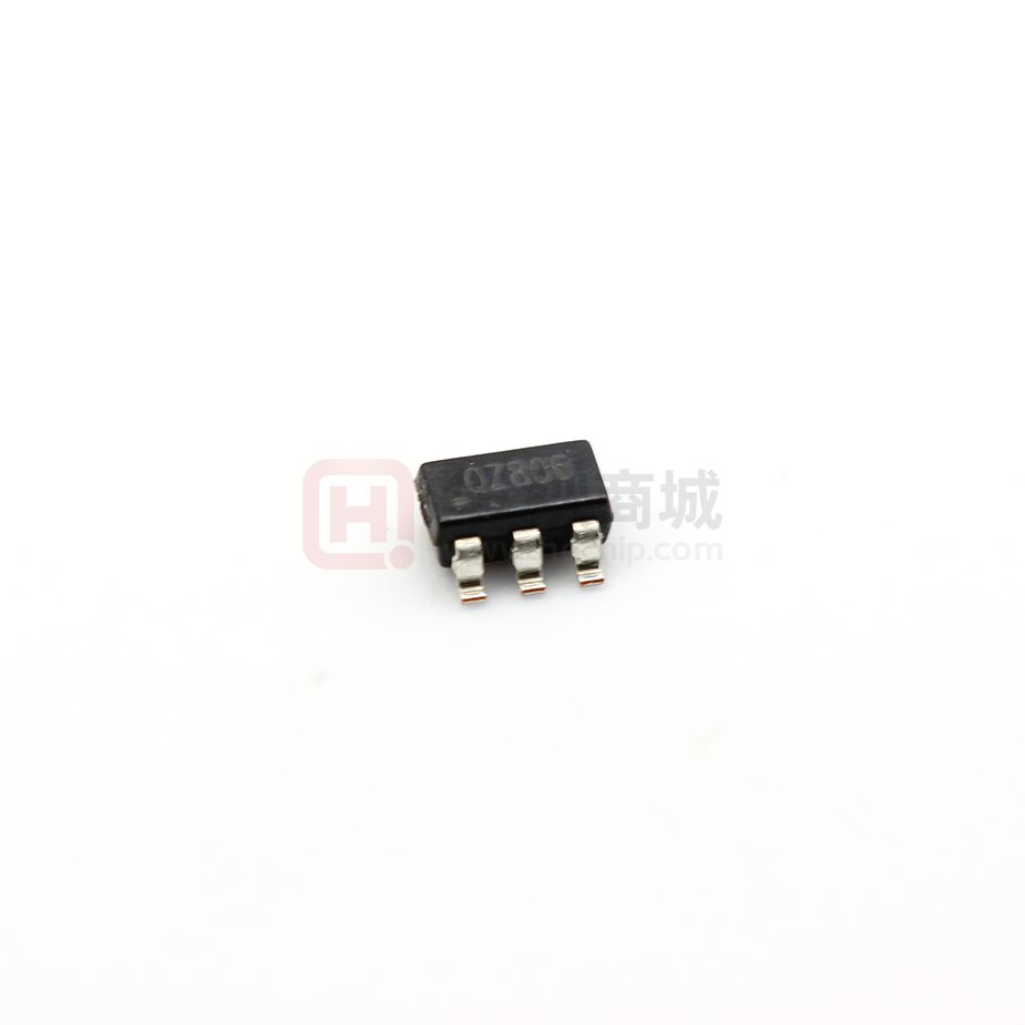
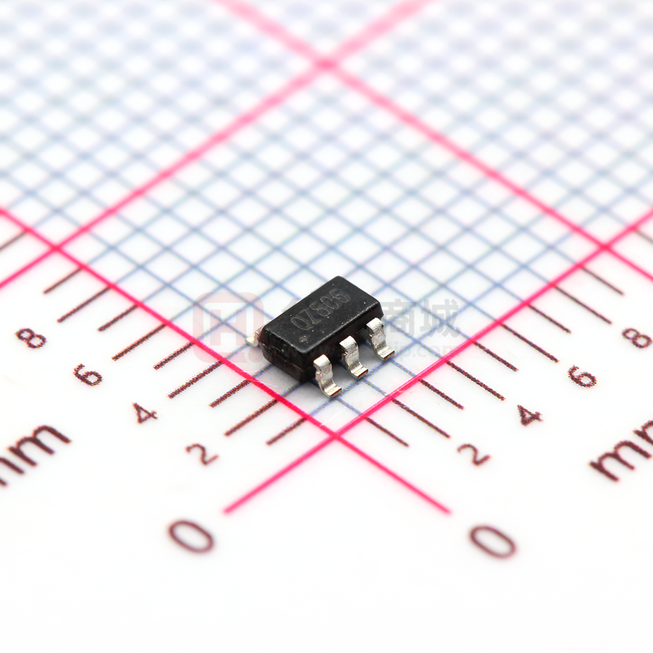
SOT23-6
D
Applications
• Load Switch
• Power Management
• Battery Protection
G
S
P-Channel MOSFET
Absolute Maximum Ratings
Parameter
Symbol
Rating
Unit
Common Ratings (TA=25°C Unless Otherwise Noted)
VDSS
Drain-Source Voltage
-20
VGSS
Gate-Source Voltage
±10
Maximum Junction Temperature
150
°C
-55 to 150
°C
TA=25°C
-1
A
TA=25°C
-20
A
TA=25°C
-5
TA=70°C
-3.1
TA=25°C
1.3
TA=70°C
0.8
TJ
TSTG
IS
Storage Temperature Range
Diode Continuous Forward Current
V
Mounted on Large Heat Sink
①
300μs Pulse Drain Current Tested
ID
②
Continuous Drain Current(VGS=-10V)
PD
Maximum Power Dissipation
IDP
RJC
RJA
③
Thermal Resistance-Junction to Case
Thermal Resistance-Junction to Ambient
A
W
-
°C/W
100
°C/W
TBD
mJ
Drain-Source Avalanche Ratings
④
EAS
Avalanche Energy, Single Pulsed
Shenzhen City Ruichips Semiconductor Co., Ltd
Rev. A– FEB., 2017
1
www.ruichips.com
�RU20P7C6
Electrical Characteristics (TA=25°C Unless Otherwise Noted)
Symbol
Parameter
Test Condition
RU20P7C6
Min.
Typ.
Max.
Unit
Static Characteristics
BVDSS
IDSS
Zero Gate Voltage Drain Current
VGS(th)
IGSS
RDS(ON)
Drain-Source Breakdown Voltage VGS=0V, IDS=-250µA
⑤
V
VDS=-20V, VGS=0V
-1
TJ=125°C
Gate Threshold Voltage
VDS=VGS, IDS=-250µA
Gate Leakage Current
VGS=±10V, VDS=0V
Drain-Source On-state Resistance
-20
µA
-30
-0.4
-1.1
V
±100
nA
VGS=-4.5V, IDS=-5A
20
25
mΩ
VGS=-2.5V, IDS=-4A
30
35
mΩ
-1.2
V
Diode Characteristics
⑤
VSD
Diode Forward Voltage
trr
Reverse Recovery Time
Qrr
Reverse Recovery Charge
ISD=-1A, VGS=0V
ISD=-5A, dlSD/dt=100A/µs
17
ns
23
nC
Ω
⑥
Dynamic Characteristics
RG
Gate Resistance
VGS=0V,VDS=0V,F=1MHz
0.9
Ciss
Input Capacitance
640
Coss
Output Capacitance
VGS=0V,
VDS=-10V,
Frequency=1.0MHz
Crss
Reverse Transfer Capacitance
65
td(ON)
Turn-on Delay Time
9
tr
Turn-on Rise Time
td(OFF)
Turn-off Delay Time
tf
Turn-off Fall Time
Gate Charge Characteristics
16
ns
45
21
⑥
Qg
Total Gate Charge
Qgs
Gate-Source Charge
Qgd
Gate-Drain Charge
Notes:
VDD=-10V, IDS=-5A,
VGEN=-4.5V,RG=6Ω
pF
135
VDS=-16V, VGS=-4.5V,
IDS=-5A
10
nC
2
3
①Pulse width limited by safe operating area.
②Calculated continuous current based on maximum allowable junction temperature.
③When mounted on 1 inch square copper board, t≤10sec. The value in any given application
depends on the user's specific board design.
④Limited by TJmax. Starting TJ = 25°C.
⑤Pulse test;Pulse width≤300µs, duty cycle≤2%.
⑥Guaranteed by design, not subject to production testing.
Shenzhen City Ruichips Semiconductor Co., Ltd
Rev. A– FEB., 2017
2
www.ruichips.com
�RU20P7C6
Ordering and Marking Information
Device
Marking①
Package
RU20P7C6
QXYWW
SOT23-6
Packaging Quantity Reel Size Tape width
Tape&Reel
3000
7’’
8mm
① The following characters could be different and means:
X =Assembly site code
Y =Year
WW =Work Week
Shenzhen City Ruichips Semiconductor Co., Ltd
Rev. A– FEB., 2017
3
www.ruichips.com
�RU20P7C6
Typical Characteristics
Power Dissipation
1
0
5
4
3
2
1
0
0
25
50
75
100
Drain Current
6
-ID - Drain Current (A)
PD - Power (W)
2
125
VGS=-4.5V
25
150
Safe Operation Area
RDS(ON) limited
-ID - Drain Current (A)
100
10
1
10µs
100µs
1ms
10ms
0.1
DC
TA=25°C
0.01
0.01
0.1
1
10
75
100
125
150
TJ - Junction Temperature (°C)
RDS(ON) - On - Resistance (mΩ)
TJ - Junction Temperature (°C)
50
Drain Current
80
IDS=-4A
60
40
20
0
0
100
1
2
3
4
5
6
7
8
-VGS - Gate-Source Voltage (V)
-VDS - Drain-Source Voltage (V)
ZthJA - Thermal Response (°C/W)
Thermal Transient Impedance
1000
Duty=0.5, 0.2, 0.1, 0.05, 0.02, 0.01, Single Pulse
100
10
1
Single Pulse
0.1
RθJA=100°C/W
0.01
1E-05
0.0001
0.001
0.01
0.1
1
10
Square Wave Pulse Duration (sec)
Shenzhen City Ruichips Semiconductor Co., Ltd
Rev. A– FEB., 2017
4
www.ruichips.com
�RU20P7C6
Typical Characteristics
Output Characteristics
-4.5V
-3V
20
-2.5V
15
-2V
10
5
-1V
0
0
1
2
3
4
Drain-Source On Resistance
80
5
RDS(ON) - On Resistance (mΩ)
-ID - Drain Current (A)
25
60
VGS=-2.5V
40
20
VGS=-4.5V
0
0
2
4
-VDS - Drain-Source Voltage (V)
2.0
Drain-Source On Resistance
1.5
1.0
TJ=25°C
Rds(on)=20mΩ
1
-25
0
25
50
75
100
125
TJ=150°C
TJ=25°C
0.1
0.01
0.0
-50
0.2
150
0.4
Capacitance
-VGS - Gate-Source Voltage (V)
C - Capacitance (pF)
Frequency=1.0MHz
800
Ciss
600
400
Coss
Crss
1
10
-VDS - Drain-Source Voltage (V)
Shenzhen City Ruichips Semiconductor Co., Ltd
Rev. A– FEB., 2017
5
0.8
1
1.2
1.4
Gate Charge
1000
0
0.6
-VSD - Source-Drain Voltage (V)
TJ - Junction Temperature (°C)
200
10
Source-Drain Diode Forward
10
VGS=-4.5V
IDS=-5A
0.5
8
-ID - Drain Current (A)
-IS - Source Current (A)
Normalized On Resistance
2.5
6
100
5
VDS=-16V
IDS=-5A
4
3
2
1
0
0
5
10
15
QG - Gate Charge (nC)
www.ruichips.com
�RU20P7C6
Avalanche Test Circuit and Waveforms
Switching Time Test Circuit and Waveforms
Shenzhen City Ruichips Semiconductor Co., Ltd
Rev. A– FEB., 2017
6
www.ruichips.com
�RU20P7C6
Package Information
SOT23-6
θ
SYMBOL
A
A1
A2
b
c
D
E
E1
e
e1
L
θ
MM
MIN
0.950
0.000
0.900
0.300
0.080
2.800
1.500
2.600
1.800
0.300
0°
NOM
1.150
0.060
1.100
0.400
0.140
2.900
1.600
2.800
0.950BSC
1.900
0.450
4°
INCH
MAX
1.450
0.150
1.300
0.500
0.200
3.050
1.750
3.000
MIN
0.037
0.000
0.035
0.012
0.003
0.110
0.059
0.102
2.000
0.600
8°
0.071
0.012
0°
Shenzhen City Ruichips Semiconductor Co., Ltd
Rev. A– FEB., 2017
7
NOM
0.045
0.002
0.043
0.016
0.006
0.114
0.063
0.110
0.037BSC
0.075
0.018
4°
MAX
0.057
0.006
0.051
0.020
0.008
0.120
0.069
0.118
0.079
0.024
8°
www.ruichips.com
�RU20P7C6
Customer Service
Worldwide Sales and Service:
Sales@ruichips.com
Technical Support:
Technical@ruichips.com
Investor Relations Contacts:
Investor@ruichips.com
Marcom Contact:
Marcom@ruichips.com
Editorial Contact:
Editorial@ruichips.comm
HR Contact:
HR@ruichips.com
Legal Contact:
Legal@ruichips.com
Shen Zhen RUICHIPS Semiconductor CO., LTD
4th Floor, Block 8, Changyuan New Material Port, Keyuan Middle Road, Science & Industry Park,
Nanshan District, Shenzhen, CHINA
TEL: (86-755) 8311-5334
FAX: (86-755) 8311-4278
E-mail: Sales-SZ@ruichips.com
Shenzhen City Ruichips Semiconductor Co., Ltd
Rev. A– FEB., 2017
8
www.ruichips.com
�


 工商网监
湘ICP备2023018690号
工商网监
湘ICP备2023018690号
