1-1-3 DC/DC Converter ICs
SPI-8001TW/SPI-8002TW/SPI-8003TW 2-Output, Step-down Switching Mode
■Features
• 2 regulators combined in one package • Output current: 1.5A × 2 (HSOP 16 Pin Surface mount package) • High efficiency: TYP80% (SPI-8001TW), TYP78% (SPI-8002TW) • Variable output voltage: 1.0 to 16V (SPI8001TW), 1.0 to 24V (SPI-8002TW) • Built-in reference oscillator (250kHz): Enables to downsize a choke-coil • Low circuit current consumption: ≤ 1µA (at output OFF) • High accuracy reference voltage: ± 1% • Built-in foldback-overcurrent and thermal protection circuits • Built-in ON/OFF circuit (soft start available) – per output
Parameter Symbol VIN Input Voltage Power Dissipation*2, *3 Junction Temperature Storage Temperature Thermal Resistance (junction to case)*2 Thermal Resistance (junction to ambient air)*2 VCC VC/E PD Tj Tstg +135 –40 to +135 9.0 35.8 SPI-8001TW 21 21 21
■Absolute Maximum Ratings*1
Ratings SPI-8002TW 40 40 40 3.0 +150 –40 to +150 SPI-8003TW 40 40 40 Unit V V V W °C °C °C/W °C/W
θ j-c θ j-a
*1: Absolute maximum ratings show the destructive limit. No parameter should exceed the ratings in transient or normal operations. *2: When mounted on glass-epoxy board 70cm2 (copper laminate area 30.8cm2). *3: Limited by thermal protection.
■Applications
• Onboard local power supplies • OA equipment • For stabilization of the secondary-side output voltage of switching power supplies
■Recommended Operating Conditions*1
Ratings Parameter Symbol VIN Input Voltage Range Output Voltage Range Output Current Range Operating Junction Temperature Range Operating Temperature Range VCC VC/E VO IO Tjop Top –30 –30 1 SPI-8001TW min. VO+3 4.5 max. 20 20 20 16 1.5 +135 +135 –30 –30 1 SPI-8002TW min. VO+3 4.5 max. 38 38 38 24 1.5 +135 +135 –30 –30 1 SPI-8003TW min. VO+3 4.5 max. 38 38 38 24 1.5 +125 +85 V V V V A °C °C Unit
*1: Recommended operating conditions show the operating conditions required for the normal circuit function described in the electrical characteristics. These conditions must be followed in actual use.
58
ICs
�SPI-8001TW/SPI-8002TW/SPI-8003TW
■Electrical Characteristics*1
Ratings Parameter Symbol min. Reference Voltage Temperature Coefficient of Reference Voltage Efficiency 1*2 Efficiency 2*2 Oscillation Frequency Line Regulation Load Regulation Overcurrent Protection Starting Current Quiescent Circuit Current 1 Quiescent Circuit Current 2 Quiescent Circuit Current 3 Quiescent Circuit Current 4 Quiescent Circuit Current 5 Quiescent Circuit Current 6 High Level Voltage C/E Pin Low Level Voltage Inflow Current at High Low Level Voltage SS Pin*3 Inflow Current at Low VREF Conditions ∆VREF/∆T Conditions Eff1 Conditions Eff2 Conditions fosc Conditions VLINE Conditions VLOAD Conditions IS Conditions IIN Conditions ICC Conditions IIN (off) Conditions ICC (off) Conditions IIN (ssov) Conditions ICC (ssov) Conditions VC/EH Conditions VC/EL Conditions IC/EH Conditions VSSL Conditions ISSL Conditions 60 0.5 VIN=VCC=15V 80 VSSL=0V, VIN=VCC=15V 60 80 95 VC/E=20V 0.5 VIN=VCC=14V 60 VSSL=0V, VIN=VCC=14V 80 2 0.8 VIN=VCC=15V 95 8.5 VCC=15V, IO=0A 1 VIN=15V, VC/E=0V or Open 1 VCC=15V, VC/E=0V or Open — — — — 2 VIN=VCC=15V 0.8 VIN=VCC=14V 95 VC/E=20V 0.5 2 VIN=VCC=14V 0.8 1 4 VIN=14V, VCC=5V, IO=0A, SS1=SS2=0V 8.5 VCC=14V, IO=0V, SS1=SS2=0V 1 4 1.6 10 30 ± 0.1 80 83 250 60 VIN=VCC=10 to 20V, VO=5V, IO=1A 40 1.6 VIN=VCC=15V 4 VIN=15V, VCC=5V, IO=0V, VO≤12V 8.5 10 40 1.6 VIN=VCC=14V 4 VIN=14V, VCC=5V, IO=0A, VO≤12V 8.5 VCC=14V, IO=0A 1 VIN=14V, VC/E=0V or Open 1 VIN=14V, VC/E=0V or Open VIN=VCC=15V, VO=5V, IO=0.2 to 1.5A 215 0.996 SPI-8001TW typ. 1.006 max. 1.016 min. 0.996 SPI-8002TW typ. 1.006 ± 0.1 78 81 250 30 285 60 200 30 10 max. 1.016 min. 0.966 SPI-8003TW typ. 1.006 VIN=14V, IO=0.1A ± 0.1 VIN=14V, IO=0.1A, Ta=–30 to +125°C 78 VIN= VCC=14V, VO=5V, IO=0.5A, IIN : including ICC 81 VIN=14V, VCC=5V, VO=5V, IO=0.5A, IIN : excluding ICC 400 60 40 VIN=14V, IO=0.1A, COSC=100pF VIN=VCC=9 to 18V, VO=5V, IO=1A VIN=VCC=14V, VO=5V, IO=0.2 to 1.5A max. 1.016
(Ta=25°C) Unit
VIN=10V, VO=1V, IO=0.1A VIN=10V, VO=1V, IO=0.1A, Ta=–30 to +135°C VIN=VCC=15V, VO=5V, IO=0.5A, IIN: including ICC VIN=15V, VO=5V, IO=0.5A, VCC=5V, IIN: excluding ICC VIN=VCC=15V, VO=5V, IO=0.5A
V mV/ °C % % kHz mV mV A mA mA
µA µA
mA mA V V
µA
V
µA
*1: Electrical characteristics show the characteristic ratings guaranteed when operating the ICs under the measurement conditions described in the above table. *2: Efficiency is calculated from the following formula.
η (%) = VO·IO × 100 VIN·IIN *3: Pin 6 and pin 11 are the SS pins. Soft start at power on can be performed with capacitors connected to these pins. The outputs can also be turned ON/OFF with these pins. The outputs are stopped by setting the voltages of these pins to VSSL or lower. SS-pin voltages can be changed with open-collector drive circuits of transistors. When using both the soft-start and ON/OFF functions together, the discharge currents from C4 and C5 flow into the ON/OFF control transistors respectively. Therefore, limit the currents securely to protect the transistors if C4 and C5 capacitances are large. The SS pins are pulled up to the power supply in the ICs, so applying the external voltages are prohibited.
ICs
59
�1-1-3 DC/DC Converter ICs
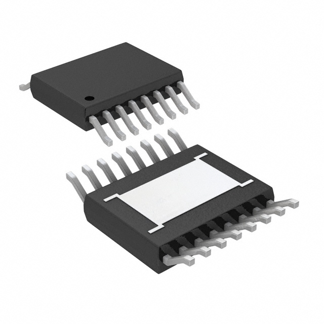
■External Dimensions (HSOP16)
1+0.1/–0.05 (Heatsink thickness) 10.5±0.2 16 9 1.35±–0.2 (Between the root of leads and back side)
(Unit : mm)
0 to 0.1
2.0+0.2/–0.08
10.5±0.3
0 to 8°
2.75MAX
1
8
2.5±0.2
Enlarged View of A A 0.25+0.15/–0.05
S 12.2±–0.2 (Gate remains: Not included in dimensions) (11)
0.10
S
16
9
Pin Assignment (SPI-8001TW, SPI-8002TW) q AGND o AGND !0 VREF2 w VIN1 e VCC !1 SS2 r SWout1 !2 DGND2 t DGND1 !3 SWout2 y SS1 !4 C/E !5 VIN2 u VREF1 i N.C !6 N.C
(2)
0.9±0.3
Pin Assignment (SPI-8003TW) q AGND w VIN1 e VCC r SWout1 t DGND1 y SS1 u VREF1 i COSC
o !0 !1 !2 !3 !4 !5 !6
AGND ROSC VREF2 SS2 DGND2 SWout2 C/E VIN2
1.27±0.25
(4.5)
0.4+0.15/–0.05
7.5±0.2
Product Mass : Approx.0.86g
■Block Diagram
VIN
+ +
VIN 3 VCC
3 VCC
SPI-8001TW/SPI-8002TW
C1
C6
SPI-8003TW
C1
C4
VC/E
14 C/E
3V
Start
VREF
1V
PReg
OSC RESET
fdown
TSD
UVLO
VC/E
15
C/E
3V
Start
VREF
1V
PReg
OSC RESET
fdown
TSD
UVLO
10 VIN1
Rosc VIN1 Cosc
2 R7
8
2
f down cut
3V
OCP
C9
f down cut
SS1
+ – +
3V
OCP
6 R5 C4 7
SS1
+ + – + – –
PWM Logic
–
Drive
SWOUT1 DGND1 VIN2 4 5 15
6 L1 Di1
+
VO1 C2 R1 R2 C7
R5 7 C5 VREF1
PWM Logic
– + – –
Drive
SWOUT1 DGND1 VIN2 4 5 16
L1 Di1
+
VO1 C2 R1 R2 C7
VREF1
Buffer-Amp
Amp
PWM
Buffer-Amp
Amp
PWM
f down cut
AGND 3V
OCP
f down cut
AGND 3V
OCP
11 R6 C5 10
SS2 VREF2
+ – + – + – –
PWM Logic
Buffer-Amp Amp PWM
Drive
SWOUT2 13 12
12 L2 Di2 DGND2
+
SS2 VREF2
+ – – + + – –
VO2 C3 C8
R6
11
PWM Logic
Buffer-Amp Amp PWM
Drive
SWOUT2 14 13
L2 Di2
+
VO2 C3 C8
AGND
C6
AGND 1, 9 R3 R4
AGND
DGND2 AGND 1, 9
R3 R4
60
ICs
�SPI-8001TW/SPI-8002TW/SPI-8003TW
■Typical Connection Diagram
VIN 3 VCC 2 VIN1 Ch1 VREF1 5 DGND1 SPI-8000TW 15 VIN2 SWout2 13 V02 L2 11 R6 SS2 Ch2 10 Di2 R3
+
VC/E 14 C/E SWout1 4 L1 V01 Di1 R1
+
VIN 3 VCC 2 VIN1 Ch1 VREF1 5 DGND1 SPI-8003TW 16 VIN2 SWout2 14 7 15 C/E SWout1 4 L1
VC/F
VC1 Di1 R1
+
6 R5
SS1
6
C2 C7
7
SS1
R5
C2 IREF1 R2
C7
IREF1
R2
C4
+
C5
+
C6
C1
C4
C1
VC2 L2 Di2 R3
+
12
C3 C8
SS2
VREF2
Ch2
12
R6
VREF2
11
DGND2 AGND 1, 9
IREF2
13
C3 DGND2 AGND 1, 9 8 C9 CORC RCSC 10 R7 IREF2 R4
C8
R4
C5 GND
C6
GND
C1 C2, C3 C4, C5 C6, C7, C8
: 220 µF/50V : 470 µF/25V : 1 µF : 0.1 µF
R5, R6 L1, L2 Di1, Di2 (Sanken)
: 1kΩ : 47 µH : SJPB-H6
GND
GND
C1 C2, C3 C4 C5, C6 C7, C8
: 220 µF/50V : 470 µF/25V : 1 µF/50V : 1 µF/10V : 0.1 µF/50V
C9 L1, L2 R2, R4 R5, R6 Di1, Di2
: 100pF/10V : 47 µH : 1kΩ : 1kΩ : SJPB-H6 (Sanken)
Diodes Di1, Di2 • Be sure to use Schottky-barrier diodes for Di1 and Di2. If other diodes like fast recovery diodes are used, IC may be destroyed because of the reverse voltage generated by the recovery voltage or ON voltage. Choke coils L1, L2 • If the winding resistance of the choke coil is too high, the efficiency may drop below the rated value. • As the overcurrent protection starting current is about 2.0A, take care concerning heat radiation from the choke coil caused by magnetic saturation due to overload or short-circuited load. • Use a closed-magnetic-path coil to prevent interference between the channels SWout1 and SWout2. Capacitors C1, C2, C3 • As large ripple currents flow through C1, C2 and C3, use high-frequency and low-impedance capacitors suitable for switching mode power supplies. Especially when the impedance of C2 and C3 are high, the switching waveforms may become abnormal at low temperatures. For C2 and C3, do not use capacitors with extremely low equivalent series resistance (ESR) such as OS capacitors or tantalum capacitors, which may cause abnormal oscillation. Resistors R1, R2, R3, R4 • R1, R2, R3 and R4 are resistors for setting output voltages. Set the resistors so that IREF is approx. 1 mA. For example, R1 and R2 can be calculated as shown below.
R1=
(VO1–VREF1) (VO1–V) VREF1 1 . =1(KΩ) = (Ω), R2= = 1×10⁻³ IREF1 1×10⁻³ . IREF1
To create the optimum operating conditions, place the components as close as possible to each other.
■Ta-PD Characteristics
3.5
θ j-a (Copper Laminate Area) 35.8°C/W (30.8 cm2)
3.0
38.2°C/W (15.6 cm2) 42.6°C/W (8.64 cm2)
Power Dissipation PD (W)
PD = VO·IO
2.5
52.3°C/W (3.34 cm2)
100 VO –1 – VF·IO 1– ηχ VIN
2.0
69.2°C/W (0.84 cm2)
1.5 1.0 0.5 0.0 –25
VO : VIN : IO : ηχ : VF :
Output Voltage Input Voltage Output Current Efficiency (%) D1 Forward Voltage SJPB-H6···0.45V (IO=1A)
0
25
50
75
100
125 135 150
Ambient Temperature Ta (°C)
Note 1: The efficiency depends on the input voltage and the output current. Therefore, obtain the value from the efficiency graph and substitute the percentage in the formula above. Note 2: Thermal design for D1 must be considered separately.
ICs
61
�


 工商网监
湘ICP备2023018690号
工商网监
湘ICP备2023018690号
