SGM25701A
Positive High-Voltage Hot Swap and Inrush
Current Controller with Power-Limiting
GENERAL DESCRIPTION
FEATURES
The SGM25701A is a positive hot swap controller that
allows a board to be safely inserted or removed from a
live backplane. Inrush current control function can
effectively reduce the voltage drop on the power supply
rail.
● Wide Input Voltage Range: 9V to 70V
● Inrush Current Limit, PCB can be Safely Inserted
into Live Equipment
● External Device Programming Maximum Loss
The SGM25701A offers programmable power-limiting
and current limit to ensure that the external MOSFET
operates within its safe operating area (SOA) at all
times.
The chip has a good output indication function when
the VOUT increases to within the 1.4V range of the VIN.
●
Programmable under-voltage lockout or over-voltage
lockout is used to turn off the device if the VIN drops
below or raises over a threshold value. The fault
detection time and initial insertion delay time can also
be adjusted by the user.
●
●
●
●
When a fault is detected, the device will go into
auto-retry mode.
APPLICATIONS
SGM25701A is available in a Green MSOP-10
package.
24V/48V Industrial Systems
Server Backplane Systems
Solid State Circuit Breaker
Base Station
TYPICAL APPLICATION
RSENSE
VIN
CIN
Limit
Programmable Current Limit
Adjustable Under-Voltage Lockout (EN/UVLO)
Adjustable Over-Voltage Lockout (OVLO)
Open-Drain for Good Output Indication
Quick Cut-Off Function when Severe
Over-Current Occurs
Configure Charge Pump/Gate Driver for External
N-MOSFET
The Setting of the Insertion Time Allowing the
Ringing and Transient Recovery Process after
the System Connected
Adjustable Fault Timing to Prevent False Shutdown
Retry Behavior after Fault: Auto-Retry
Available in a Green MSOP-10 Package
●
●
●
●
●
VOUT
Z1
Onl y requi red wh en
using SS star tup.
M1
1kΩ
R1
R3
VIN
SENSE
GATE
EN/UVLO
OVLO
R2
D2
D1
COUT
3.6MΩ (1)
CSS
Q2
OUT
VDD
SGM25701A
R4
100kΩ
PG
PWR
RPWR
GND
TIMER
CTIMER
NOTE: 1. The resistance provides a stable leaking path for the GATE pin when the VIN is quickly pulled low in the case of
repeated restarts.
Figure 1. Typical Application Circuit
SG Micro Corp
www.sg-micro.com
DECEMBER 2022 – REV. A
Downloaded From Oneyac.com
�Positive High-Voltage Hot Swap and Inrush
Current Controller with Power-Limiting
SGM25701A
PACKAGE/ORDERING INFORMATION
MODEL
PACKAGE
DESCRIPTION
SPECIFIED
TEMPERATURE
RANGE
ORDERING
NUMBER
PACKAGE
MARKING
PACKING
OPTION
SGM25701A
MSOP-10
-40℃ to +125℃
SGM25701AXMS10G/TR
SGM004
XMS10
XXXXX
Tape and Reel, 4000
MARKING INFORMATION
NOTE: XXXXX = Date Code, Trace Code and Vendor Code.
XXXXX
Vendor Code
Trace Code
Date Code - Year
Green (RoHS & HSF): SG Micro Corp defines "Green" to mean Pb-Free (RoHS compatible) and free of halogen substances. If
you have additional comments or questions, please contact your SGMICRO representative directly.
ABSOLUTE MAXIMUM RATINGS
(1)
VIN to GND .................................................. -0.3V to 80V
SENSE, OUT and PG to GND .......................... -0.3V to 80V
GATE to GND (1) .............................................. -0.3V to 80V
OUT to GND (1ms Transient) (2) .......................... -1V to 80V
EN/UVLO to GND ............................................ -0.3V to 80V
OVLO to GND.................................................... -0.3V to 6V
VIN to SENSE ................................................ -0.3V to 0.3V
Package Thermal Resistance
MSOP-10, θJA ..................................................... 147℃/W
MSOP-10, θJB ....................................................... 94℃/W
MSOP-10, θJC ....................................................... 52℃/W
Junction Temperature .............................................. +150℃
Storage Temperature Range ...................... -65℃ to +150℃
Lead Temperature (Soldering, 10s) .......................... +260℃
ESD Susceptibility
HBM ......................................................................... 2000V
CDM ......................................................................... 1000V
NOTES:
1. When the chip is enabled, the voltage of GATE pin is
generally 12.7V higher than the VIN pin voltage. Therefore,
the absolute maximum rating of VIN (80V) is only applicable
when the chip is stopped, or since the absolute maximum
rating of the GATE pin is also 80V, the 80V of VIN is only
applicable when the pin is momentarily surged.
2. An external MOSFET with VGS_TH higher than VOUT is
required during -ve transients. This effectively prevents false
turn-on of the MOSFET during -ve transients.
RECOMMENDED OPERATING CONDITIONS
Supply Voltage, VIN .............................................. 9V to 70V
PG Voltage .......................................................... 0V to 70V
Junction Temperature Range...................... -40℃ to +125℃
OVERSTRESS CAUTION
Stresses beyond those listed in Absolute Maximum Ratings
may cause permanent damage to the device. Exposure to
absolute maximum rating conditions for extended periods
may affect reliability. Functional operation of the device at any
conditions beyond those indicated in the Recommended
Operating Conditions section is not implied.
ESD SENSITIVITY CAUTION
This integrated circuit can be damaged if ESD protections are
not considered carefully. SGMICRO recommends that all
integrated circuits be handled with appropriate precautions.
Failure to observe proper handling and installation procedures
can cause damage. ESD damage can range from subtle
performance degradation to complete device failure. Precision
integrated circuits may be more susceptible to damage
because even small parametric changes could cause the
device not to meet the published specifications.
DISCLAIMER
SG Micro Corp reserves the right to make any change in
circuit design, or specifications without prior notice.
SG Micro Corp
www.sg-micro.com
DECEMBER 2022
2
Downloaded From Oneyac.com
�Positive High-Voltage Hot Swap and Inrush
Current Controller with Power-Limiting
SGM25701A
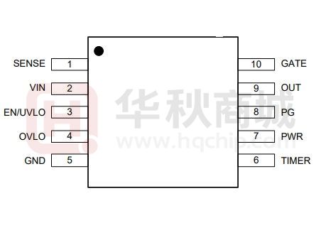
PIN CONFIGURATION
(TOP VIEW)
SENSE
1
10
GATE
VIN
2
9
OUT
EN/UVLO
3
8
PG
OVLO
4
7
PWR
GND
5
6
TIMER
MSOP-10
PIN DESCRIPTION
PIN
NAME
I/O
FUNCTION
1
SENSE
I
Current Sense Pin. The voltage from the input pin to this pin is measured by the current flowing
into the sense resistor. When the detected voltage at the RSENSE exceeds 55mV, it indicates that
the circuit is in an overload state at this time, and the fault timer is started at this time.
2
VIN
I
Input Supply Voltage. It is recommended to place a small bypass capacitor close this pin.
3
EN/UVLO
I
4
OVLO
I
5
GND
-
6
TIMER
I/O
7
PWR
I
8
PG
O
9
OUT
I
10
GATE
O
Enable and Under-Voltage Lockout Pin. The EN/UVLO threshold is programmed by an external
resistor divider. Internal hysteresis is controlled by a 19µA current source. The threshold of the
turn-on voltage is set to 2.5V. It is also possible to control this pin for remote shutdown.
Over-Voltage Lockout Pin. The over-voltage threshold is programmed by the resistor divider
from the power supply to the OVLO terminal to GND. Hysteretic control is achieved through an
internally programmed 19µA current source. The over-voltage shutdown threshold is set to
2.5V.
Ground.
Fault Timer Pin. An external capacitor between TIMER and GND pins provides the fault time
delay and insertion delay time. The chip's restart time is also controlled by this capacitor.
Power-Limiting Programmable Pin. The RPWR and RSENSE determine the maximum allowable
dissipation of the external MOSFET.
Power Good Indicator Pin. The VDS voltage of the external MOSFET determines its state.
Power Output Pin. Connect this pin to output (i.e., external MOSFET source). The chip monitors
MOSFET VDS voltage through this pin to limit the MOSFET power and control the PG signal
accordingly.
Gate Drive Output. This pin is connected to the gate of the external MOSFET. During normal
operation, the voltage on this pin will be 12.7V higher than the OUT pin.
SG Micro Corp
www.sg-micro.com
DECEMBER 2022
3
Downloaded From Oneyac.com
�Positive High-Voltage Hot Swap and Inrush
Current Controller with Power-Limiting
SGM25701A
ELECTRICAL CHARACTERISTICS
(TJ = -40℃ to +125℃, typical values are at TJ = +25℃, VIN = 48V, unless otherwise noted.)
PARAMETER
SYMBOL
CONDITIONS
MIN
TYP
MAX
UNITS
0.40
0.55
mA
VIN
Input Current, Enabled
IIN_EN
VEN/UVLO > 2.5V and VOVLO < 2.5V
Input Current, Disabled
IIN_DIS
VEN/UVLO < 2.5V or VOVLO > 2.5V
70
110
µA
PORIT
VIN increasing
7.6
8.1
V
POREN
VIN increasing
8.4
9.0
V
POREN_HYS
VIN decreasing
90
Power-On Reset Threshold at VIN
to Trigger Insertion Timer
Power-On Reset Threshold at VIN
to Enable All Functions
POREN Hysteresis
mV
OUT
OUT Bias Current, Enabled
OUT Bias Current, Disabled
(1)
IOUT_EN
VOUT = VIN, normal operation
6
IOUT_DIS
Disabled, VOUT = 0V, VSENSE = VIN
25
µA
EN/UVLO, OVLO
EN/UVLO Threshold Voltage
VEN/UVLO
EN/UVLO Hysteresis Current
IEN/UVLO_HYS
EN/UVLO Delay Time
tEN/UVLO_DLY
EN/UVLO Bias Current
VEN/UVLO = 1V
2.4
2.5
2.6
V
12
19
26
µA
Delay to GATE high
15
Delay to GATE low
1
VEN/UVLO_BIAS VEN/UVLO = 48V
OVLO Threshold Voltage
VOVLO
OVLO Hysteresis Current
IOVLO_HYS
2.4
VOVLO = 2.6V
12
1
µA
2.5
2.6
V
19
26
µA
Delay to GATE high
15
Delay to GATE low
1
OVLO Delay Time
tOVLO_DLY
OVLO Bias Current
VOVLO_BIAS
VOVLO = 2.4V
PWRLIM-1
V(SENSE - OUT) = 48V, RPWR = 150kΩ
µs
µs
1
µA
31
mV
PWR
Power-Limiting Sense Voltage
(VIN - SENSE)
PWR Pin Current
PWRLIM-2
IPWR
19
25
V(SENSE - OUT) = 24V, RPWR = 75kΩ
25
mV
VPWR = 2.5V
20
µA
GATE Pin
Source Current
Sink Current
Gate Output Voltage in Normal
Operation
IGATE
VGATE
Normal operation, V(GATE - OUT) = 5V
10
16
22
µA
VEN/UVLO < 2.5V
1.8
2.1
2.4
mA
V(VIN - SENSE) = 150mV or VIN < PORIT, VGATE = 5V
55
85
115
mA
12.2
12.7
13.2
V
GATE - OUT voltage
NOTE: 1. A 1MΩ resistor between OUT and SENSE pins determines the bias current (disabled) of VOUT.
SG Micro Corp
www.sg-micro.com
DECEMBER 2022
4
Downloaded From Oneyac.com
�Positive High-Voltage Hot Swap and Inrush
Current Controller with Power-Limiting
SGM25701A
ELECTRICAL CHARACTERISTICS (continued)
(TJ = -40℃ to +125℃, typical values are at TJ = +25℃, VIN = 48V, unless otherwise noted.)
PARAMETER
SYMBOL
CONDITIONS
MIN
TYP
MAX
UNITS
48.5
55.0
61.5
mV
Current Limit
Threshold Voltage
VCL
VIN - SENSE voltage
Response Time
tCL
VIN - SENSE stepped from 0mV to 80mV
10
Enabled, VSENSE = VOUT
12
Disabled, VOUT = 0V
70
SENSE Input Current
ISENSE
µs
µA
Circuit Breaker
Threshold Voltage
Response Time
VCB
VIN - SENSE voltage
tCB
VIN - SENSE stepped from 0mV to 150mV, time to
GATE low, no load
80
105
130
mV
0.4
1.2
µs
3.85
4.00
4.15
V
1.20
1.25
1.30
V
TIMER
Upper Threshold
VTMRH
Lower Threshold
VTMRL
Restart cycles
End of 8th cycle
Insertion Time Current
Sink Current, End of Insertion Time
Fault Detection Current
ITIMER
VTIMER = 2V
Fault Sink Current
Fault Restart Duty Cycle
DCFAULT
Fault to GATE Low Delay
tFAULT
0.3
3
5
1.2
70
1.5
TIMER pin reaches 4V
V
7
µA
1.6
2.0
mA
95
120
µA
2.4
3.3
µA
0.43
%
1
µs
PG
Decreasing
0.8
1.4
2.0
Increasing, relative to decreasing threshold
0.8
1.4
2.0
85
150
mV
2
µA
Threshold Measured at SENSE OUT
PGTH
Output Low Voltage
PGVOL
ISINK = 2mA
Off Leakage Current
PGIOH
VPG = 70V
SG Micro Corp
www.sg-micro.com
V
DECEMBER 2022
5
Downloaded From Oneyac.com
�Positive High-Voltage Hot Swap and Inrush
Current Controller with Power-Limiting
SGM25701A
FUNCTIONAL BLOCK DIAGRAM
PG
PWR
SGM25701A
-
+
20μA
VIN
1.4V/2.8V
-
OUT
+
1MΩ
Power-Limiting
Threshold
VDS
Charge
Pump
+
-
SENSE
VIN
ID
Gate
Control
+
+
55mV
GATE
2.1mA
85mA 12.7V
-
VOUT
Current Limit
Threshold
19μA
OVLO
16μA
Current Limit/
Power-Limiting Control
+
-
2.5V
5μA
Insertion
Timer
+
2.5V
-
UVLO
95μA
Fault
Timer
TIMER
1.6mA
End of
Insertion
Time
19μA
-
7.6V
Insertion Timer POR
Timer and Gate
Logic Control
2.4μA Fault
Discharge
+
VIN
+
8.4V/8.3V
+
-
Enable POR
4V
1.25V
+
0.3V
-
-
GND
Figure 2. Block Diagram
SG Micro Corp
www.sg-micro.com
DECEMBER 2022
6
Downloaded From Oneyac.com
�Positive High-Voltage Hot Swap and Inrush
Current Controller with Power-Limiting
SGM25701A
TYPICAL PERFORMANCE CHARACTERISTICS
TJ = +25℃ and VIN = 48V, unless otherwise noted.
VIN Pin Input Current vs. VIN Voltage
100
SENSE Pin Input Current (μA)
VIN Pin Input Current (mA)
1.0
0.8
0.6
Enable, EN/UVLO = VIN
0.4
0.2
0.0
Disable, EN/UVLO = 0V
0
10
20
30
40
50
60
80
Disable, EN/UVLO = 0V
60
40
20
0
70
SENSE Pin Input Current vs. SENSE Pin Voltage
Enable, EN/UVLO = VIN
0
10
VIN Voltage (V)
GATE - OUT Voltage (V)
OUT Pin Current (μA)
40
Disable, EN/UVLO = 0V
20
0
-20
Enable, EN/UVLO = VIN
0
10
20
30
40
50
60
6
3
PG Pin Output Low Voltage (V)
GATE Pin Source Current (μA)
8
0
10
20
Enabled, EN/UVLO = VIN
Normal Operation
30
40
POREN
0
10
20
Enabled, EN/UVLO = VIN
Normal Operation
30
40
50
60
70
50
60
PG Pin Output Low Voltage vs. Sink Current
1
12
0
70
VIN Voltage (V)
16
POREN
60
9
0
70
GATE Pin Source Current vs. VIN Voltage
4
50
12
VIN Voltage (V)
20
40
GATE Pin Voltage vs. VIN Voltage
15
Load at OUT Pin = 600Ω
Current flow is out of the pin
60
30
SENSE Pin Voltage (V)
OUT Pin Current vs. VIN Voltage
80
20
70
0.8
0.6
0.4
0.2
0
0
VIN Voltage (V)
3
6
9
12
15
18
21
PG Sink Current (mA)
SG Micro Corp
www.sg-micro.com
DECEMBER 2022
7
Downloaded From Oneyac.com
�Positive High-Voltage Hot Swap and Inrush
Current Controller with Power-Limiting
SGM25701A
TYPICAL PERFORMANCE CHARACTERISTICS (continued)
MOSFET Power Dissipation Limit vs. RPWR
250
GATE Pull-Down Current, Circuit Breaker vs. GATE Pin Voltage
100
RSENSE = 0.1Ω
RSENSE = 0.05Ω
RSENSE = 0.02Ω
RSENSE = 0.01Ω
RSENSE = 0.005Ω
200
150
GATE Pull-Down Current,
Circuit Breaker (mA)
MOSFET Power Dissipation Limit (W)
TJ = +25℃ and VIN = 48V, unless otherwise noted.
100
50
0
80
60
40
20
0
25
50
75
100
125
0
150
RPWR (kΩ)
OVLO Hysteresis Current (μA)
EN/UVLO Hysteresis Current (μA)
19
18
17
-50
-25
0
25
50
20
30
75
100
OVLO
17
-50
-25
0
-25
0
25
50
25
50
75
100
125
75
100
125
Input Current, Enabled vs. Temperature
0.41
0.4
0.39
0.38
0.37
-50
80
18
0.42
Input Current, Enabled (mA)
EN/UVLO, OVLO Threshold Voltage (V)
EN/UVLO
2.49
2.48
70
Temperature (℃)
2.52
2.50
60
19
16
125
EN/UVLO, OVLO Threshold Voltage vs. Temperature
2.51
50
20
Temperature (℃)
2.53
40
OVLO Hysteresis Current vs. Temperature
21
20
16
10
GATE Pin Voltage (V)
EN/UVLO Hysteresis Current vs. Temperature
21
0
-50
-25
0
25
50
75
100
125
Temperature (℃)
Temperature (℃)
SG Micro Corp
www.sg-micro.com
DECEMBER 2022
8
Downloaded From Oneyac.com
�Positive High-Voltage Hot Swap and Inrush
Current Controller with Power-Limiting
SGM25701A
TYPICAL PERFORMANCE CHARACTERISTICS (continued)
TJ = +25℃ and VIN = 48V, unless otherwise noted.
Current Limit Threshold vs. Temperature
55.0
54.5
54.0
53.5
53.0
-50
-25
0
25
50
75
100
Circuit Breaker Threshold vs. Temperature
110
Circuit Breaker Threshold
Voltage Across RSENSE (mV)
Current Limit Threshold
Voltage Across RSENSE (mV)
55.5
108
106
104
102
100
125
-50
-25
0
Temperature (℃)
GATE Output Voltage above OUT Pin
(V)
Power-Limiting Threshold
Voltage Across RSENSE (mV)
125
12.6
25.5
12.4
25.0
12.2
-50
-25
0
25
50
75
100
125
12.0
-50
-25
0
Temperature (℃)
16.8
16.6
16.4
16.2
GATE - OUT = 5V
-25
0
25
50
Temperature (℃)
50
75
100
125
GATE Pull-Down Current, Circuit Breaker vs. Temperature
110
75
100
125
GATE Pull-Down Current, Circuit Breaker
(mA)
GATE Source Current vs. Temperature
-50
25
Temperature (℃)
17.0
GATE Source Current (μA)
100
GATE - OUT Voltage,
Normal Operation
12.8
26.0
16.0
75
GATE Output Voltage vs. Temperature
13.0
26.5
24.5
50
Temperature (℃)
Power-Limiting Threshold vs. Temperature
27.0
25
100
90
80
70
GATE = 5V
60
-50
-25
0
25
50
75
100
125
Temperature (℃)
SG Micro Corp
www.sg-micro.com
DECEMBER 2022
9
Downloaded From Oneyac.com
�Positive High-Voltage Hot Swap and Inrush
Current Controller with Power-Limiting
SGM25701A
TYPICAL PERFORMANCE CHARACTERISTICS (continued)
TJ = +25℃ and VIN = 48V, unless otherwise noted.
PG Output Low Voltage vs. Temperature
PG Output Low Voltage (mV)
110
100
90
80
70
60
PG Sink Current = 2mA
-50
-25
0
25
50
75
100
125
Temperature (℃)
SG Micro Corp
www.sg-micro.com
DECEMBER 2022
10
Downloaded From Oneyac.com
�Positive High-Voltage Hot Swap and Inrush
Current Controller with Power-Limiting
SGM25701A
TYPICAL PERFORMANCE CHARACTERISTICS (continued)
TJ = +25℃ and VIN = 36V, unless otherwise noted.
Start-Up
Start-Up (Zoomed In)
10V/div
10V/div
VOUT
VGATE
5V/div
5V/div
VGATE
VTIMER
VIN
10V/div
10V/div
VOUT
10V/div
10V/div
VIN
VTIMER
Time (100ms/div)
Time (5ms/div)
Start-Up into Short-Circuit
Under-Voltage Lockout
VIN
VOUT
10V/div
10V/div 5V/div
VGATE
VTIMER
10V/div
1A/div
IIN
10V/div
10V/div
VIN
VGATE
Time (10ms/div)
Time (10ms/div)
Over-Voltage Lockout
Gradual Over-Current
10A/div
20V/div
IIN
20V/div
20V/div
VGATE
VIN
VGATE
5V/div
VOUT
20V/div
20V/div
VIN
VTIMER
Time (20ms/div)
Time (5ms/div)
SG Micro Corp
www.sg-micro.com
DECEMBER 2022
11
Downloaded From Oneyac.com
�Positive High-Voltage Hot Swap and Inrush
Current Controller with Power-Limiting
SGM25701A
TYPICAL PERFORMANCE CHARACTERISTICS (continued)
TJ = +25℃ and VIN = 36V, unless otherwise noted.
Load Step
Hot-Short on Output
VIN
VGATE
5V/div
5V/div
VTIMER
20V/div
20V/div
VGATE
IIN
20V/div
20V/div
VIN
20A/div
10A/div
IIN
VTIMER
Time (10ms/div)
Time (10ms/div)
Hot-Short (Zoomed In)
Auto-Retry
VIN
VGATE
5V/div
20V/div
VTIMER
20V/div
20V/div
VGATE
20V/div
20V/div
VOUT
20A/div
20A/div
IIN
IIN
VTIMER
Time (5μs/div)
Time (1s/div)
SG Micro Corp
www.sg-micro.com
DECEMBER 2022
12
Downloaded From Oneyac.com
�SGM25701A
Positive High-Voltage Hot Swap and Inrush
Current Controller with Power-Limiting
DETAILED DESCRIPTION
Overview
The SGM25701A is designed to limit the generated
inrush current when the circuit card is plugged into and
removed from the live backplane or hot power supply,
reduce the voltage sag and dV/dt on the load during
power-on, and avoid unnecessary reset and other
impacts. The SGM25701A not only has current limit
function, but also detects power dissipation when used
in series to ensure the operations within SOA. Once the
current limit or power-limiting exceeds the preset value,
the SGM25701A components will repeatedly try to
recover until the faults are removed. When the input
voltage range exceeds EN/UVLO and OVLO ranges,
the device breaks during the period.
Current Limit
The device triggers over-current protection when the
voltage on the RSENSE reaches the current limit
threshold of 55mV. In this event, the device limits the
current in M1 by controlling GATE pin, and the TIMER
pin is active. If the current is lower than the threshold
before the fault timeout period ends, the device
recovers. Note that RSENSE cannot be larger than
100mΩ.
Circuit Breaker
Once the load current rises rapidly, the current on
RSENSE may exceed the current limit value before the
current limit control loop responds. When the current on
RSENSE exceeds two times the current limit value, M1 is
pulled down by the 85mA current source to turn off
quickly, and the fault timeout starts timing until the
voltage on RSENSE drops below 105mV. If VTIMER
reaches 4V before current limit or power-limiting
ceases, M1 will be pulled off by the 2.1mA current
source.
Power-Limiting
The power-limiting ensures that the power dissipation
(MAX) of M1 is within the SOA of the SGM25701A. The
device defines the power dissipation of the M1 by
sensing the VDS of the M1 and the drain current flowing
through RSENSE. The current and voltage values will be
compared to the resistor that is used to program the
power-limiting value on the PWR pin. The fault timer is
activated if the power-limiting circuit is active.
EN/UVLO and OVLO
M1 starts to work when the power supply voltage (VIN)
operates between the under-voltage lockout value and
the over-voltage lockout value programmed by the
resistor network (R1, R2, R3 and R4). When the input
supply voltage is lower than the EN/UVLO threshold,
the 19µA current sink inside the EN/UVLO is enabled,
the current source inside the OVLO is turned off, and
M1 is kept off by the 2.1mA current source pull-down of
the GATE pin. As the input supply voltage increases,
when VEN/UVLO exceeds 2.5V, its internal 19µA current
sink turns off to increase the EN/UVLO voltage,
providing a threshold of hysteresis when M1 is enabled
by the 16µA current source at GATE pin. The EN/UVLO
pin can be connected to VIN to set the minimum
EN/UVLO level, when the VIN reaches the power-on
reset threshold (POREN), M1 is enabled. When the
power supply voltage rises so that the voltage on the
OVLO pin exceeds 2.5V, M1 is pulled down by the
2.1mA current source at GATE pin. At this time, the
OVLO pin voltage is higher than 2.5V, the internal 19µA
current source is turned on, and the VOVLO is decreased
to provide threshold hysteresis. Please refer to the
application and implementation to calculate the
resistance value of R1 ~ R4 to program the threshold.
SG Micro Corp
www.sg-micro.com
DECEMBER 2022
13
Downloaded From Oneyac.com
�Positive High-Voltage Hot Swap and Inrush
Current Controller with Power-Limiting
SGM25701A
DETAILED DESCRIPTION (continued)
Power Good Pin
The PG pin remains high during the turn-on period until
the VIN increases above ≊ 1V. At this time, as VIN
increases, PG continues to pull low. When the VOUT
increases to within 1.4V of the SENSE pin voltage, (VDS
< 1.4V), PG is switched high. If VDS of M1 increases
above 2.8V, PG switches low. PG requires a pull-up
resistor and the pull-up voltage (VPG) may be as high as
70V for transient capability up to 80V. If PG requires a
delay, please refer to Figure 3. Capacitor CPG adds a
delay to the rising edge in Figure 3 (1). The slew rate of
the rising edge is determined by RPG1 + RPG2 and CPG,
and the slew rate of the falling edge is determined by
RPG2 and CPG in Figure 3 (2). Add a diode as shown in
Figure 3 (3) to achieve an equal slope of rising edge
and falling edge. For most applications, the typical
values in Figure 3 (2) are recommended: RPG1 = 100kΩ,
RPG2 = 0Ω, CPG = 1μF.
VPG
SGM25701A
RPG1
Power Good
PG
CPG
GND
(1)
VPG
SGM25701A
RPG1
Power Good
PG
RPG2
CPG
GND
(2)
VPG
SGM25701A
RPG1
PG
Power Good
RPG2
CPG
GND
(3)
Figure 3. Adding Delay to the Power Good Output Pin
The SGM25701A has a power-up sequence that can
be divided into 3 distinct parts: insertion time, inrush
limit and normal operation. Once in normal operation,
the TIMER and GATE pins depend on whether the
output has a fault condition.
Power-Up Sequence
The SGM25701A has an input voltage range of 9V to
70V, and the transient input can reach 80V. Please
refer to Figure 4 for details of this section. When the
input voltage begins to increase, a strong pull-down
85mA current source inside the GATE pin prevents the
Miller capacitance of the MOSFET from being charged.
Furthermore, the TIMER pin is pulled low until the VIN
reaches the PORIT threshold. At this time, between
insertions, the CTIMER begins to be charged by the
internal 5μA current source when the M1 is still turned
off by the internal 2.1mA current source without being
affected by VIN. VIN is allowed to stabilize gradually
during the insertion time. When the voltage of the
TIMER pin reaches 4V, the insertion time is over, and
the charge on the CTIMER is quickly discharged by the
internal 1.6mA current source. After the insertion time,
when the VIN reaches the power-on reset threshold
(POREN), the control circuit is enabled. If the input
voltage exceeds the under-voltage lockout threshold,
the 16μA current source inside the GATE pin starts to
work and turns on M1, and the VGS of M1 is limited to
12.7V by the internal Zener diode. When the OUT pin
voltage increases, the SGM25701A detects the drain
current and power dissipation of the M1, and enables
the current limit circuit and power-limiting circuit. During
the inrush limit period, the CTIMER is charged by the
internal 95μA current source at the TIMER pin. If the
power dissipation on M1 and the input current decrease
below their respective limit thresholds before the CTIMER
voltage value reaches 4V, the 95μA current source is
turned off and the charge of the CTIMER is discharged by
the internal 2.4μA current sink.
When the OUT pin voltage increases to within 1.4V of
the input voltage, the current limit interval is completed
and the PG pin is pulled high. If the voltage of TIMER
pin reaches 4V before the current limit or power-limiting
ceases, the TIMER pin will be enabled and the GATE
pin of M1 will be pulled low by the internal 2.1mA
current source and shut down until the next power-up
sequence starts or the restart sequence ends.
SG Micro Corp
www.sg-micro.com
DECEMBER 2022
14
Downloaded From Oneyac.com
�Positive High-Voltage Hot Swap and Inrush
Current Controller with Power-Limiting
SGM25701A
DETAILED DESCRIPTION (continued)
VIN UVLO
PORIT
0V
4V
TIMER
0.3V
0V
GATE
85mA
Pull-Down
2.4μA
95μA
5μA
1.6mA
16μA Source
2.1mA Pull-Down
Current Limit
Load Current
OUT
1.4V
PG
Normal Operation
Insertion Time
Inrush
Limit
Figure 4. Power-Up Sequence (Power-Limiting Only)
Gate Control
An internal charge pump can provide an internal bias
higher than the output voltage to boost the gate of the
N-MOSFET. The VGS of M1 is limited to 12.7V by an
internal Zener diode. During normal operation (see
Figure 4), the GATE pin is charged to approximately
12.7V above the OUT pin by the internal 16μA current
source. If the maximum gate-source voltage of the
external N-MOSFET is less than 12.7V, a low voltage
Zener diode with a forward current of at least 100mA
must be added outside the device. A strong pull-down
current source of 85mA for the initial operation of the
device can prevent M1 from being mis-turned through
the drain-to-gate capacitance.
mode and the TIMER will be discharged by the internal
2.4μA current. When the TIMER pin is charged to 4V,
and the device is still in current limit or power-limiting
state, the load cannot be started properly. The GATE
will continue to be pulled down by the 2.1mA current
source and enter the restart sequence. The GATE pin
is also pulled down by the 2.1mA current source when
the supply voltage is lower than EN/UVLO threshold
voltage or above OVLO threshold voltage. Please refer
to Figure 5 for the detailed structure.
RSENSE
VIN
When the system is initially powered up, the GATE pin
is pulled low by an internal 85mA current source to
prevent misleading MOSFET on through the drain-gate
capacitance. The GATE pin is pulled low by a 2.1mA
current source in insertion time (see Figure 4) while the
MOSFET is always turned off. During the following
inrush limit time (see Figure 4), the voltage of the GATE
pin is limited to the programmed current or
power-limiting level when the TIMER pin is charged by
the 95μA current source. If SGM25701A exits current
limit or power-limiting state before the TIMER pin is
charged to 4V, the circuit will enter normal operating
SG Micro Corp
www.sg-micro.com
VOUT
COUT
Q1
SENSE
VIN
GATE
OUT
Charge
Pump
Gate
Control
Current Limit/
Power-Limiting
Control
2.1mA
Fault/
UVLO/
OVLO/
Insertion
Time
85mA
Circuit Breaker/
Initial Hold
Down
Figure 5. Gate Control
DECEMBER 2022
15
Downloaded From Oneyac.com
�Positive High-Voltage Hot Swap and Inrush
Current Controller with Power-Limiting
SGM25701A
DEVICE FUNCTIONAL MODELS (continued)
Shutdown Control
In addition, the remote control device can be turned off
and safely started by connecting an open collector
device or an open-drain device on the EN/UVLO pin, as
shown in the Figure 6.
VSYS
VIN
R1
EN/UVLO
R2
Shutdown
SGM25701A
OVLO
R3
GND
Figure 6. Shutdown Control
Fault Timer and Restart
When the current limit or power-limiting value is
reached during the startup process, the GATE pin
voltage is limited to regulate the load current and
power dissipation. Then a 95μA current source will
charge the TIMER, please refer to the Figure 7. If the
current or power-limiting situation fades before the
TIMER pin is charged to 4V, the device enters normal
operation mode. Otherwise, the GATE pin of M1 will be
continuously pulled low by the 2.1mA current source.
The TIMER pin is discharged by the 2.4μA current sink
and enters a restart sequence of repeated charge and
discharge. After seven failure timeout cycles, the restart
sequence ends when the voltage of the eighth descent
ramp of the TIMER pin drops below 0.3V, and the 16μA
current source of the GATE pin turns on M1. If the fault
persists, the restart sequence will be repeated.
Fault Detection
Current Limit
Load
Current
2.1mA Pull-Down
GATE
16μA Source
4V
TIMER
2.4μA
95μA
1.25V
Fault Timeout Period
1
2
3
7
8
0.3V
tRESTART
Figure 7. Restart Sequence
SG Micro Corp
www.sg-micro.com
DECEMBER 2022
16
Downloaded From Oneyac.com
�Positive High-Voltage Hot Swap and Inrush
Current Controller with Power-Limiting
SGM25701A
APPLICATION INFORMATION
The SGM25701A is a hot swap controller used for fault
case protections and inrush current management.
Consider startup, hot-short and start-into-short
scenarios in detail before proceeding with applications.
In addition, for the safety of the equipment and systems,
please carefully review the SOA (safe operating area)
section of the choice of MOSFET. It is recommended to
use the SGM25701A design calculator provided in the
datasheet. The following design cases and calculation
formulas can be used for reference.
help dissipate heat. The following example uses a
value of 30℃/W, which is similar to SGM25701A EVB.
The test conditions for hot swap are needed to know
before the test. The design must ensure that the
MOSFET is safe even if the output is shorted. It is
recommended not to carry the load until the MOSFET
is successfully started. Loading the MOSFET too early
may cause the startup failure.
RSENSE
VIN
Typical Application
RSENSE
VIN
CIN
Q1
Z1
Only required when
using SS startup.
M1
1kΩ
R1
R3
VIN
SENSE
GATE
D2
D1
SENSE
GATE
COUT
OUT
PG
3.6MΩ (1)
SGM25701A
CSS
Q2
CL
RL
GND
EN/UVLO
OVLO
R2
VIN
VOUT
OUT
VDD
SGM25701A
R4
100kΩ
Figure 9. No Load Current during Turn-On
PG
PWR
GND
RPWR
TIMER
CTIMER
Table 1. Design Parameters
Figure 8. Typical Application Schematic (36V/11A)
Design Requirements
Table 1 lists the necessary parameters which are
needed to know before designing. The power
dissipation of the hot swap MOSFET during startup is
stored in the output capacitor. Therefore, the VIN and
COUT value determine the stress of the MOSFET. The
selection of sense resistor is determined by the
maximum operating load current. Additionally, the
maximum operating load current, ambient temperature,
and thermal characteristics of the PCB (RθCA), all affect
the RDSON requirements and the number of power
MOSFETs used. The RθCA value is extremely sensitive
to copper area and PCB layout. Note that the drain is
not electrically grounded, so the ground plane does not
Parameter
Value
Input Voltage
24V to 48V
Operating Load Current (MAX)
11A
Lower EN/UVLO Threshold
22V
Upper EN/UVLO Threshold
24V
Lower OVLO Threshold
48V
Upper OVLO Threshold
50V
Load Capacitance (MAX)
1000µF
Ambient Temperature (MAX)
85℃
MOSFET RθCA
(Function of Layout)
30℃/W
SG Micro Corp
www.sg-micro.com
Pass Hot-Short on Output.
Pass A Start into Short.
The Load is Off until PG Asserted.
A Hot Board cannot be Plugged Back in.
DECEMBER 2022
17
Downloaded From Oneyac.com
�Positive High-Voltage Hot Swap and Inrush
Current Controller with Power-Limiting
SGM25701A
APPLICATION INFORMATION (continued)
Detailed Design Procedure
Select RSENSE and CL Setting
The device measures real-time current by monitoring
the voltage across the RSENSE. When the voltage across
RSENSE exceeds 55mV, the GATE pin is pulled low. Note
the power and size of the RSENSE and the selected
over-current value. Use Equation 1 to calculate the
appropriate sense resistance.
RSENSE
=
VCL 55mV
=
= 5mΩ
ILIM
11A
(1)
Selecting the Hot Swap MOSFET(s)
Selecting the right MOSFET for hot swap applications
is critical. Please ensure that the device meets the
requirements as below:
When using multiple MOSFETs in parallel, please use
Equation 4 as below.
TC,MAX = TA,MAX + RθCA × (
The SOA of the MOSFET can meet the following
scenarios: startup, hot-short, and start-into-short.
Try to keep the RDSON as small as possible to avoid
excessive temperature rise. It recommends a
steady state of less than +125℃ for MOSFETs.
The maximum continuous current must be greater
than the maximum load current, and the drain
pulse current must be greater than the threshold
current of the circuit breaker.
For the design, the KNB2710A is selected. The
maximum steady state case temperature can be
calculated as Equation 2 after selecting the MOSFET.
2
TC,MAX = TA,MAX + RθCA × ILOAD,MAX
× RDSON,MAX (TJ )
ILOAD,MAX
# of MOSFETs
)2 × RDSON (TJ )
VSENSE =
PLIM × RSENSE
VDS
=
PLIM,MIN
VSENSE,MIN × VIN,MAX 5mV × 48V
= = 48W
RSENSE
5mΩ
(6)
It can further calculate the corresponding minimum
RPWR at this power-limiting according to Equation 7.
RPWR = 1.30 × 10⁵ × RSENSE × (PLIM - 1.18mV ×
VDS
)
RSENSE
(7)
Note that the minimum RPWR corresponds to the VDS =
VIN,MAX. It can be calculated by Equation 8.
RPWR = 1.30 × 105 × 5mΩ × (48W - 1.18mV ×
TC,MAX.
(5)
VSENSE below 5mV is not recommended to avoid low
power-limiting accuracy. In this application, it can use
Equation 6 to calculate the corresponding
power-limiting value.
(2)
Note that RDSON is a strong function of junction
temperature. According to the KNB datasheet, RDSON is
about 1.4× at 85℃. Equation 3 is used to calculate
(4)
Select Power-Limiting
It is usually best to use power-limiting to reduce stress
on the MOSFET. However, when the power-limiting is
set very low and the current flowing through the
MOSFET is controlled, the voltage across the RSENSE
will very low. Equation 5 can be used to calculate the
voltage across the RSENSE.
The VDS of the MOSFET can withstand the
maximum input voltage of the system along with
the ringing introduced during transients.
If the calculated temperature value of a single MOSFET
is too high, the power dissipation can be dispersed by
increasing the number of MOSFETs.
48V
) = 24kΩ (8)
5mΩ
For a more accurate power-limiting, select a
power-limiting value lager than 48W. It can use a
slightly larger resistance of 33kΩ, which sets a
power-limiting of 62.1W.
TC,MAX = 85℃ + 30℃/W × (11A)2 × (1.4 × 4.5mΩ) = 107.87℃ (3)
SG Micro Corp
www.sg-micro.com
DECEMBER 2022
18
Downloaded From Oneyac.com
�Positive High-Voltage Hot Swap and Inrush
Current Controller with Power-Limiting
SGM25701A
APPLICATION INFORMATION (continued)
Set Fault Timer
Please ensure that the fault timer has enough time to
ensure that it does not time out in the power-limiting or
current limit operation during this period. If the device is
running in current limit state from the start, the
maximum startup time can be calculated by Equation 9.
t START,MAX =
COUT × VIN,MAX
ILIM
(9)
For this example, the device enters a conversion from
power-limiting to current limit during startup. The
startup time can be estimated according to Equation
10.
V2
C
P
t START =OUT × IN,MAX + 2LIM
2
ILIM
PLIM
2
1000μF (48V) 62.1W
+
=
×
2
2
62.1W (11A)
(10)
= 18.81ms
Please note that the time calculated above is the ideal
constant power conversion to constant current startup.
Because power-limiting is a function of VDS, the actual
startup time will be longer than calculated time. In
addition, it needs to consider errors introduced by some
device specifications, such as CTIMER and constant
current source, power-limiting value, etc., and also
needs an additional 50% time margin to ensure that the
startup time does not time out. Therefore, use Equation
11 to determine the value of the fault timer capacitance.
=
CTIMER
tFLT × ITIMER(TYP)
18.81ms × 95μA
=
× 1.5
=
× 1.5 670nF (11)
VTIMER(TYP)
4V
The capacitor of 680nF with a slightly larger
capacitance can be selected to calculate the
programming time of the fault timer according to
Equation 12.
CTIMER × VTIMER,TYP 680nF × 4V
=
= = 28.6ms
tFLT
ITIMER,TYP
95μA
Check MOSFET SOA
Once the power-limiting and timer capacitance values
are selected, it is important to confirm the SOA
characteristics of the MOSFET. SOA characteristics
describe how long a MOSFET can safely operate at a
certain current under a VDS. In the worst case, the
MOSFET operates in a power-limiting state all the time.
The current flowing value is PLIM/VIN,MAX and the
duration is tFLT. Taking this application as an example, it
must ensure that the MOSFET may handle 1A at 48V
for 28.9ms. Based on the SOA of the KNB2710A, it can
handle 48V, 19A for 1ms and it can handle 48V, 5A for
100ms. Refer to Equations 13 to 15 to calculate the
corresponding safe working period.
| (t )
19A
ln SOA 1
ln(
)
ISOA (t 2 )
5A
m =
-0.29
=
=
t
1ms
ln(
)
ln( 1 )
100ms
t2
=
a
ISOA (t1 )
19A
=
= 19A × (1ms)0.29
t1m
(1ms)-0.29
ISOA (28.9ms) =
19A × (1ms)0.29 × (28.9ms)-0.29
= 7.163A
If the system has not started successfully beyond this
time, the SGM25701A will shut down the KNB2710A
MOSFET.
(14)
(15)
(16)
Note that the current calculated above is an ideal
calculation considering the MOSFET case temperature
to be +25 ℃ . A certain ambient temperature and
thermal increase during operation can make the
MOSFET more possible to hot-short. It can use
Equation 17 to calculate the approximate current.
=
ISOA
(28.9ms,TC,MAX ) ISOA (28.9ms,25℃) ×
= 7.163A ×
= 3.21A
(12)
(13)
lSOA (t)= a × t m
TJ,ABSMAX - TC,MAX
IJ,ABSMAX - 25℃
(17)
175℃ - 107.87℃
175℃ - 25℃
Based on this calculation, the MOSFET can handle
3.21A, 48V for 28.9ms at elevated case temperature.
This value is larger than the 1.29A required for
power-limiting startup, indicating that there is little risk
of hot-short to the MOSFET during startup. It is
recommended that the selected MOSFET may
calculate an equivalent current value that exceeds the
required value by 1.3× to provide sufficient margin.
SG Micro Corp
www.sg-micro.com
DECEMBER 2022
19
Downloaded From Oneyac.com
�Positive High-Voltage Hot Swap and Inrush
Current Controller with Power-Limiting
SGM25701A
APPLICATION INFORMATION (continued)
Set Under-Voltage and Over-Voltage Threshold
By setting the EN/UVLO and OVLO thresholds,
SGM25701A turns on the main power MOSFET M1
when the input voltage is within the normal operating
range. Conversely, M1 switches off, stopping the output
current.
VUVL =
EN/UVLO
R2
2.5V
19μA
19μA
R3
OVLO
2.5V
R4
GND
Figure 10. Programming the Four Thresholds
Use the following Equations 18 and 19 to calculate the
upper and lower threshold of EN/UVLO.
=
R1
VUVH - VUVL VUV(HYS)
=
19μA
19μA
(18)
2.5V × R1
(VUVL - 2.5V)
R2 =
(19)
Use the following Equations 20 and 21 to calculate the
upper and lower threshold of OVLO.
VOVH - VOVL VOV(HYS)
=
R3 =
19μA
19μA
R4 =
2.5V × (R3 + R 4 )
R4
(25)
(27)
Component Values
Table 2 provides the selected device values under the
condition of 36V/11A, and the application curve is also
based on these device values.
Table 2. Component Values
Component
Value
RSENSE
5mΩ
R1
100kΩ
(21)
R2
13kΩ
R3
100kΩ
R4
5.6kΩ
VUVH = 24V, VUVL = 22V, VOVH = 50V, and VOVL = 48V.
Therefore, VUV(HYS) = 2V and VOV(HYS) = 2V.
RPWR
33kΩ
M1
KNB2710A
The resistor values are: R1 = 100kΩ, R2 = 13kΩ, R3 =
100kΩ, and R4 = 5.6kΩ.
Z1
SMBJ70A-13-F
D1
MBRS3100T3G
Under the condition that R1 - R4 is calculated, the
threshold voltage and hysteresis voltage are calculated
using Equation 22 to Equation 27.
VUVH= 2.5V + [R1 × (
2.5V
+ 19μA)]
R2
(26)
Input and Output Protection
The SGM25701A needs to connect voltage clamping
devices on the input side under hot plug conditions. It is
necessary to select an appropriate TVS as shown in
Figure 1. When the hot plug circuit is suddenly pulled
out of the socket under the load condition, TVS needs
to suppress the voltage surge at this time. The principle
of TVS selection is that there is a small leakage current
at VIN(MAX), and it is clamped below the set voltage when
the input surge voltage is large.
(20)
2.5V × R3
(VOVH - 2.5V)
2.5V
- 19μA)]
R4
VOV(HYS)
= R3 × 19μA
Timer and
Gate
Logic
Control
+
R1
(24)
VOVL = 2.5V + [R3 × (
SGM25701A
+
VIN
VSYS
(23)
VUV(HYS)
= R1 × 19μA
VOVH =
The four thresholds can be accurately calculated using
the configuration shown in Figure 10.
2.5V × (R1 + R2 )
R2
CTIMER
680nF
COUT
1000μF
(22)
SG Micro Corp
www.sg-micro.com
DECEMBER 2022
20
Downloaded From Oneyac.com
�Positive High-Voltage Hot Swap and Inrush
Current Controller with Power-Limiting
SGM25701A
APPLICATION INFORMATION (continued)
Power Supply Recommendations
Generally speaking, SGM25701A can provide stable
power supply with reliable performance. However,
when other card slots on the backplane are inserted,
the high frequency dynamics on the backplane will
appear. When this happens in the system, it is
recommended to place a capacitor of 1μF on the drain
of MOSFET. This will reduce the common mode
voltage between VIN and SENSE pins, which needs to
be suppressed to prevent over-current shutdown.
The RSENSE needs to be close to the controller chip
and use the Kelvin connection.
The current path and return path from the input to
the load side should be parallel and close to each
other to reduce the loop inductance.
GND of components around SGM25701A can be
connected with each other and connected with
GND pin of SGM25701A. Then connect GND to
the system ground uniformly. Do not separately
connect the ground of the devices around the chip
to the ground of the system with high current.
PCB layout provides good heat dissipation
conditions for MOSFET M1 to reduce the junction
temperature when it is turned on and off.
PC Board Guidelines
SGM25701A should observe the following principles
when laying PCB:
SGM25701A needs to be placed near the input
connector to reduce the lead inductance from the
connector to the power MOSFET.
System Considerations
The bypass capacitor of VIN should be placed carefully.
When MOSFET is turned off due to short-circuit, the
input terminal has a very large dV/dt. When the
capacitor is placed close to the VIN pin, the LC filter is
formed due to the long routing from SENSE to VIN. At
this time, a large voltage difference may be formed
between VIN and SENSE. To prevent this, place the
capacitor on the RSENSE terminal instead of VIN
terminal.
As shown in Figure 12, the normal operation of
SGM25701A requires a capacitor on the backplane
side. The capacitor with live backplane needs to absorb
the input surge voltage generated when the controller
cuts off the load. If there is no capacitance, TVS needs
to be placed in the input measurement to prevent large
voltage generated during voltage transient from
exceeding the maximum rated value of VIN pin.
When the output of SGM25701A is inductive load, it is
necessary to reverse parallel diode on the load side.
When the load is cut off, a reverse path is provided for
the current of the inductive load to prevent negative
voltage from damaging the device.
√
Trace
Inductance
SENSE
×
VIN
SGM25701A
Figure 11. Layout Trace Inductance
RSENSE
+48V
Live
Backplane
M1
SENSE
VOUT
GATE
OUT
VCC
SGM25701A
CL
Inductive
Load
GND
GND
Plug-In Board
Figure 12. Output Diode Required for Inductive Loads
SG Micro Corp
www.sg-micro.com
DECEMBER 2022
21
Downloaded From Oneyac.com
�SGM25701A
Positive High-Voltage Hot Swap and Inrush
Current Controller with Power-Limiting
REVISION HISTORY
NOTE: Page numbers for previous revisions may differ from page numbers in the current version.
Changes from Original (DECEMBER 2022) to REV.A
Page
Changed from product preview to production data..................................................................................................................................................... All
SG Micro Corp
www.sg-micro.com
DECEMBER 2022
22
Downloaded From Oneyac.com
�PACKAGE INFORMATION
PACKAGE OUTLINE DIMENSIONS
MSOP-10
b
E1
4.8
E
1.02
e
0.5
0.3
RECOMMENDED LAND PATTERN (Unit: mm)
D
L
A
θ
c
A1
A2
Symbol
Dimensions
In Millimeters
MIN
MAX
A
0.820
1.100
A1
0.020
A2
0.750
b
0.180
Dimensions
In Inches
MIN
MAX
0.032
0.043
0.150
0.001
0.006
0.950
0.030
0.037
0.280
0.007
0.011
c
0.090
0.230
0.004
0.009
D
2.900
3.100
0.114
0.122
E
2.900
3.100
0.114
0.122
E1
4.750
5.050
0.187
e
0.500 BSC
0.199
0.020 BSC
L
0.400
0.800
0.016
0.031
θ
0°
6°
0°
6°
NOTES:
1. Body dimensions do not include mode flash or protrusion.
2. This drawing is subject to change without notice.
SG Micro Corp
www.sg-micro.com
TX00015.000
Downloaded From Oneyac.com
�PACKAGE INFORMATION
TAPE AND REEL INFORMATION
REEL DIMENSIONS
TAPE DIMENSIONS
P2
W
P0
Q1
Q2
Q1
Q2
Q1
Q2
Q3
Q4
Q3
Q4
Q3
Q4
B0
Reel Diameter
A0
P1
K0
Reel Width (W1)
DIRECTION OF FEED
NOTE: The picture is only for reference. Please make the object as the standard.
KEY PARAMETER LIST OF TAPE AND REEL
Reel
Diameter
Reel Width
W1
(mm)
A0
(mm)
B0
(mm)
K0
(mm)
P0
(mm)
P1
(mm)
P2
(mm)
W
(mm)
Pin1
Quadrant
MSOP-10
13"
12.4
5.20
3.30
1.50
4.0
8.0
2.0
12.0
Q1
SG Micro Corp
www.sg-micro.com
TX10000.000
Downloaded From Oneyac.com
DD0001
Package Type
�PACKAGE INFORMATION
CARTON BOX DIMENSIONS
NOTE: The picture is only for reference. Please make the object as the standard.
KEY PARAMETER LIST OF CARTON BOX
Length
(mm)
Width
(mm)
Height
(mm)
Pizza/Carton
13″
386
280
370
5
SG Micro Corp
www.sg-micro.com
DD0002
Reel Type
TX20000.000
Downloaded From Oneyac.com
�单击下面可查看定价,库存,交付和生命周期等信息
>>SGMICRO(圣邦微电子)
Downloaded From Oneyac.com
�


 工商网监
湘ICP备2023018690号
工商网监
湘ICP备2023018690号

