LH75400/01/10/11
System-on-Chip
Data Sheet
DESCRIPTION
• JTAG Debug Interface and Boundary Scan
The SHARP BlueStreak LH75400/01/10/11 family
consists of four low-cost 16/32-bit System-on-Chip
(SoC) devices.
• Single 3.3 V Supply
• LH75401 — contains the superset of features.
• 144-pin LQFP Package
• LH75411 — similar to LH75401, without CAN 2.0B.
• -40° C to +85° C Operating Temperature
• LH75400 — similar to LH75401, but with a Grayscale LCDC only.
Unique Features of the LH75401
• LH75410 — similar to LH75400, without CAN 2.0B.
COMMON FEATURES
• Highly Integrated System-on-Chip
• ARM7TDMI-S™ Core
• High Performance (84 MHz CPU Speed)
– Internal PLL Driven or External Clock Driven
– Crystal Oscillator/Internal PLL Can Operate with
Input Frequency Range of 14 MHz to 20 MHz
• Clock and Power Management
– Low Power Modes: Standby, Sleep, Stop
• Eight Channel, 10-bit Analog-to-Digital Converter
• Integrated Touch Screen Controller
• Serial interfaces
– Two 16C550-type UARTs supporting baud rates
up to 921,600 baud (requires crystal frequency of
14.756 MHz).
– One 82510-type UART supporting baud rates up
to 3,225,600 baud (requires a system clock of
70 MHz).
• Real-Time Clock (RTC)
• Three Counter/Timers
– Capture/Compare/PWM Compatibility
– Watchdog Timer (WDT)
• Low-Voltage Detector
Data Sheet
• Color and Grayscale Liquid Crystal Display (LCD)
Controller
– 12-bit (4,096) Direct Mode Color, up to VGA
– 8-bit (256) Direct or Palletized Color, up to SVGA
– 4-bit (16) Direct Mode Color/Grayscale, up to XGA
– 12-bit Video Bus
– Supports STN, TFT, HR-TFT, and AD-TFT
Displays.
• CAN Controller that supports CAN version 2.0B.
Unique Features of the LH75411
• 32KB On-chip SRAM
– 16KB Tightly Coupled Memory (TCM) SRAM
– 16KB Internal SRAM
• Synchronous Serial Port
– Motorola SPI™
– National Semiconductor Microwire™
– Texas Instruments SSI
• 5 V Tolerant Digital I/O
– XTALIN and XTAL32IN inputs are 1.8 V ± 10%
• Color and Grayscale LCD Controller (LCDC)
– 12-bit (4,096) Direct Mode Color, up to VGA
– 8-bit (256) Direct or Palletized Color, up to SVGA
– 4-bit (16) Direct Mode Color/Grayscale, up to XGA
– 12-bit Video Bus
– Supports STN, TFT, HR-TFT, and AD-TFT
Displays.
Unique Features of the LH75400
• Grayscale LCDC
– 4-bit (16 Level) Grayscale, up to XGA
– 8-bit Video Bus
– Supports STN Displays.
• Controller Area Network (CAN) Controller that supports CAN version 2.0B.
Unique Features of the LH75410
• Grayscale LCDC
– 4-bit (16 Level) Grayscale, up to XGA
– 8-bit Video Bus
– Supports STN Displays.
NOTES:
1. ARM7 Thumb, and ARM7TDMI-S are trademarks of ARM LTD.
2. Motorola SPI is a trademark of Motorola, Inc.
3. Microwire is a trademark of National Semiconductor Corporation.
4. VGA and XGA modes require 66 MHz CPU speed.
5. XTAL inputs are not 5 V tolerant.
6. CPU performance at 1.8 V at 50°C, VDDC supplied externally.
Version 1.2
1
�LH75400/01/10/11
System-on-Chip
LH75401 BLOCK DIAGRAM
LH75401
14 to 29 MHz
32.768 kHz
OSCILLATOR,
PLL, POWER
MANAGEMENT, and
RESET CONTROL
INTERNAL
16KB SRAM
ARM7TDMI-S
AHB
INTERFACE
VECTORED
INTERRUPT
CONTROLLER
TCM
16KB SRAM
REAL TIME
CLOCK
76-BIT GENERAL
PURPOSE I/O
I/O
CONFIGURATION
SYNCHRONOUS
SERIAL PORT
4 CHANNEL
DMA
CONTROLLER
STATIC
MEMORY
CONTROLLER
ADVANCED
PERIPHERAL
BUS BRIDGE
COLOR
LCD
CONTROLLER
BROWNOUT
DETECTOR
ADVANCED
LCD
INTERFACE
LINEAR
REGULATOR
TIMER (3)
WATCHDOG
TIMER
CAN 2.0B
UART (3)
8 CHANNEL
10-BIT ADC
TOUCH PANEL
INTERFACE
ADVANCED HIGH
PERFORMANCE
BUS (AHB)
ADVANCED
PERPHERAL
BUS (APB)
LH75401-1
Figure 1. LH75401 Block Diagram
2
Version 1.2
Data Sheet
�System-on-Chip
LH75400/01/10/11
LH75411 BLOCK DIAGRAM
LH75411
14 to 29 MHz
32.768 kHz
OSCILLATOR,
PLL, POWER
MANAGEMENT, and
RESET CONTROL
INTERNAL
16KB SRAM
ARM 7TDMI-S
AHB
INTERFACE
VECTORED
INTERRUPT
CONTROLLER
TCM
16KB SRAM
REAL TIME
CLOCK
76-BIT GENERAL
PURPOSE I/O
I/O
CONFIGURATION
SYNCHRONOUS
SERIAL PORT
4 CHANNEL
DMA
CONTROLLER
STATIC
MEMORY
CONTROLLER
ADVANCED
PERIPHERAL
BUS BRIDGE
COLOR
LCD
CONTROLLER
BROWNOUT
DETECTOR
ADVANCED
LCD
INTERFACE
LINEAR
REGULATOR
ADVANCED HIGH
PERFORMANCE
BUS (AHB)
TIMER (3)
WATCHDOG
TIMER
UART (3)
8 CHANNEL
10-BIT ADC
TOUCH PANEL
INTERFACE
ADVANCED
PERPHERAL
BUS (APB)
LH75411-1
Figure 2. LH75411 Block Diagram
Data Sheet
Version 1.2
3
�LH75400/01/10/11
System-on-Chip
LH75400 BLOCK DIAGRAM
LH75400
14 to 29 MHz
32.768 kHz
OSCILLATOR,
PLL, POWER
MANAGEMENT, and
RESET CONTROL
INTERNAL
16KB SRAM
ARM 7TDMI-S
AHB
INTERFACE
VECTORED
INTERRUPT
CONTROLLER
TCM
16KB SRAM
REAL TIME
CLOCK
76-BIT GENERAL
PURPOSE I/O
I/O
CONFIGURATION
SYNCHRONOUS
SERIAL PORT
4 CHANNEL
DMA
CONTROLLER
STATIC
MEMORY
CONTROLLER
ADVANCED
PERIPHERAL
BUS BRIDGE
GRAYSCALE
LCD
CONTROLLER
BROWNOUT
DETECTOR
TIMER (3)
WATCHDOG
TIMER
CAN 2.0B
UART (3)
LINEAR
REGULATOR
8 CHANNEL
10-BIT ADC
TOUCH PANEL
INTERFACE
ADVANCED HIGH
PERFORMANCE
BUS (AHB)
ADVANCED
PERPHERAL
BUS (APB)
LH75400-1
Figure 3. LH75400 Block Diagram
4
Version 1.2
Data Sheet
�System-on-Chip
LH75400/01/10/11
LH75410 BLOCK DIAGRAM
LH75410
14 to 29 MHz
32.768 kHz
OSCILLATOR,
PLL, POWER
MANAGEMENT, and
RESET CONTROL
INTERNAL
16KB SRAM
ARM 7TDMI-S
AHB
INTERFACE
VECTORED
INTERRUPT
CONTROLLER
TCM
16KB SRAM
REAL TIME
CLOCK
76-BIT GENERAL
PURPOSE I/O
I/O
CONFIGURATION
SYNCHRONOUS
SERIAL PORT
4 CHANNEL
DMA
CONTROLLER
STATIC
MEMORY
CONTROLLER
ADVANCED
PERIPHERAL
BUS BRIDGE
GRAYSCALE
LCD
CONTROLLER
BROWNOUT
DETECTOR
TIMER (3)
WATCHDOG
TIMER
UART (3)
8 CHANNEL
10-BIT ADC
LINEAR
REGULATOR
ADVANCED HIGH
PERFORMANCE
BUS (AHB)
ADVANCED
PERPHERAL
BUS (APB)
TOUCH PANEL
INTERFACE
LH75410-1
Figure 4. LH75410 Block Diagram
Data Sheet
Version 1.2
5
�LH75400/01/10/11
System-on-Chip
THE LH75401
TOP VIEW
108
107
106
105
104
103
102
101
100
99
98
97
96
95
94
93
92
91
90
89
88
87
86
85
84
83
82
81
80
79
78
77
76
75
74
73
PF6/CTCAP2B/CTCMP2B
PE0/UARTRX2
VSS
PE1/UARTTX2
PE2/CANRX/UARTRX0
PE3/CANTX/UARTTX0
PE4/SSPTX
PE5/SSPRX
PE6/SSPCLK
PE7/SSPFRM
VDD
VDDA_ADC
AN0(UL/X+)/PJ0
AN6/PJ1
AN1(UR/X-)/PJ2
AN8/PJ3
AN2(LL/Y+)/PJ4
AN9/PJ5
AN4(WIPER)/PJ6
AN3(LR/Y-)/PJ7
VSSA_ADC
XTALOUT
XTALIN
VDDA_PLL
VSSA_PLL
XTAL32OUT
XTAL32IN
nPOR
VSSC
PD0/INT0
PD1/INT1
PD2/INT2
PD3/INT3/UARTTX1
VDDC
PD4/INT4/UARTRX1
PD5/INT5/DACK
144-PIN LQFP
109
110
111
112
113
114
115
116
117
118
119
120
121
122
123
124
125
126
127
128
129
130
131
132
133
134
135
136
137
138
139
140
141
142
143
144
72
71
70
69
68
67
66
65
64
63
62
61
60
59
58
57
56
55
54
53
52
51
50
49
48
47
46
45
44
43
42
41
40
39
38
37
PD6/INT6/DREQ
nRESETOUT
LINREGEN
TDO
TDI
TCK
RTCK
TMS
TEST1
TEST2
nRESETIN
A0
A1
VSS
A2
A3
A4
A5
VDD
A6
A7
A8
A9
A10
VSS
A11
A12
A13
A14
A15
VDD
VSS
PC0/A16
PC1/A17
PC2/A18
PC3/A19
PA7/D15
PA6/D14
VDD
PA5/D13
PA4/D12
PA3/D11
PA2/D10
VSS
PA1/D9
PA0/D8
VDDC
D7
D6
VSSC
D5
D4
VDD
D3
D2
D1
D0
nWE
nOE
PB5/nWAIT
PB4/nBLE1
VSS
PB3/nBLE0
PB2/nCS3
PB1/nCS2
PB0/nCS1
nCS0
PC7/A23
PC6/A22
VDD
PC5/A21
PC4/A20
1
2
3
4
5
6
7
8
9
10
11
12
13
14
15
16
17
18
19
20
21
22
23
24
25
26
27
28
29
30
31
32
33
34
35
36
PF5/CTCAP2A /CTCMP2A
PF4/CTCAP1B/CTCMP1B
PF3/CTCAP1A /CTCMP1A
VDD
PF2/CTCAP0E
PF1/CTCAP0D
PF0/CTCAP0C
PG7/CTCAP0B/CTCMP0B
PG6/CTCAP0A /CTCMP0A
PG5/CTCLK
VSS
PG4/LCDVEEEN /LCDMOD
PG3 /LCDVDDEN
PG2/LCDDSPLEN /LCDREV
PG1/LCDCLS
PG0/LCDPS
PH7/LCDDCLK
VDD
VSS
PH6/LCDLP/LCDHRLP
PH5/LCDFP/LCDSPS
PH4/LCDEN/LCDSPL
PH3/ LCDVD11
PH2/ LCDVD10
PH1/LCDVD9
VDD
PH0/LCDVD8
PI7/LCDVD7
PI6/LCDVD6
PI5/LCDVD5
PI4/LCDVD4
VSS
PI3/LCDVD3
PI2/LCDVD2
PI1/LCDVD1
PI0/LCDVD0
NOTE: Always refer to the Pin 1 mark for proper device orientation. See ‘Package Specifications’ for marking details.
LH75401-51
Figure 5. LH75401 Pin Diagram
6
Version 1.2
Data Sheet
�System-on-Chip
LH75400/01/10/11
LH75401 Numerical Pin Listing
Table 1. LH75401 Numerical Pin List
PIN
NO.
FUNCTION
AT RESET
FUNCTION
2
FUNCTION FUNCTION OUTPUT
3
TYPE
DRIVE
BUFFER
TYPE
BEHAVIOR DURING
RESET
NOTES
1
PA7
D15
I/O
8 mA
Bidirectional
Pull-up
1
2
PA6
D14
I/O
8 mA
Bidirectional
Pull-up
1
3
VDD
Power
None
4
PA5
D13
I/O
8 mA
Bidirectional
Pull-up
1
5
PA4
D12
I/O
8 mA
Bidirectional
Pull-up
1
6
PA3
D11
I/O
8 mA
Bidirectional
Pull-up
1
7
PA2
D10
Bidirectional
Pull-up
1
8
VSS
9
PA1
10
PA0
11
I/O
8 mA
Ground
None
D9
I/O
8 mA
Bidirectional
Pull-up
1
D8
I/O
8 mA
Bidirectional
Pull-up
1
VDDC
Power
None
12
D7
I/O
8 mA
Bidirectional
Pull-up
13
D6
I/O
8 mA
Bidirectional
Pull-up
14
VSSC
Ground
None
15
D5
I/O
8 mA
Bidirectional
Pull-up
16
D4
I/O
8 mA
Bidirectional
Pull-up
17
VDD
Power
None
18
D3
I/O
8 mA
Bidirectional
Pull-up
19
D2
I/O
8 mA
Bidirectional
Pull-up
20
D1
I/O
8 mA
Bidirectional
Pull-up
21
D0
I/O
8 mA
Bidirectional
Pull-up
22
nWE
8 mA
Output
HIGH
3
23
nOE
8 mA
Output
HIGH
3
24
PB5
nWAIT
8 mA
Bidirectional
Pull-up
1, 3
25
PB4
nBLE1
8 mA
Bidirectional
Pull-up
1, 3
26
VSS
27
PB3
nBLE0
8 mA
Bidirectional
Pull-up
1, 3
28
PB2
nCS3
8 mA
Bidirectional
Pull-up
1, 3
29
PB1
nCS2
8 mA
Bidirectional
Pull-up
1, 3
30
PB0
nCS1
8 mA
Bidirectional
Pull-up
1, 3
31
nCS0
8 mA
Output
Pull-up
3
1
Ground
None
32
PC7
A23
8 mA
Bidirectional
Pull-down
33
PC6
A22
8 mA
Bidirectional
Pull-down
1
34
VDD
35
PC5
A21
8 mA
Bidirectional
Pull-down
1
36
PC4
A20
8 mA
Bidirectional
Pull-down
1
37
PC3
A19
8 mA
Bidirectional
Pull-down
1
38
PC2
A18
8 mA
Bidirectional
Pull-down
1
Data Sheet
Power
None
Version 1.2
7
�LH75400/01/10/11
System-on-Chip
Table 1. LH75401 Numerical Pin List (Cont’d)
PIN
NO.
FUNCTION
AT RESET
FUNCTION
2
FUNCTION FUNCTION OUTPUT
3
TYPE
DRIVE
BUFFER
TYPE
BEHAVIOR DURING
RESET
NOTES
39
PC1
A17
8 mA
Bidirectional
Pull-down
1
40
PC0
A16
8 mA
Bidirectional
Pull-down
1
41
VSS
Ground
None
42
VDD
Power
None
43
A15
8 mA
Output
LOW
44
A14
8 mA
Output
LOW
45
A13
8 mA
Output
LOW
46
A12
8 mA
Output
LOW
47
A11
8 mA
Output
LOW
48
VSS
49
A10
8 mA
Output
LOW
50
A9
8 mA
Output
LOW
51
A8
8 mA
Output
LOW
52
A7
8 mA
Output
LOW
53
A6
8 mA
Output
LOW
54
VDD
55
A5
8 mA
Output
LOW
56
A4
8 mA
Output
LOW
57
A3
8 mA
Output
LOW
8 mA
Output
LOW
Ground
Power
None
None
58
A2
59
VSS
60
A1
8 mA
Output
LOW
61
A0
8 mA
Output
LOW
62
nRESETIN
None
Input
Pull-up
2, 3
63
TEST2
None
Input
Pull-up
2
64
TEST1
None
Input
Pull-up
2
65
TMS
None
Input
Pull-up
2
66
RTCK
4 mA
Output
67
TCK
None
Input
68
TDI
None
Input
Pull-up
2
69
TDO
4 mA
Output
70
LINREGEN
None
Input
5
71
nRESETOUT
8 mA
Output
3
72
PD6
INT6
DREQ
6 mA
Bidirectional
73
PD5
INT5
DACK
6 mA
Bidirectional
74
PD4
INT4
UARTRX1
8 mA
Bidirectional
Pull-up
1
75
VDDC
76
PD3
INT3
8 mA
Bidirectional
Pull-up
1
77
PD2
INT2
2 mA
Bidirectional
Pull-up
1
Ground
Power
UARTTX1
None
Pull-down
1
1, 2
None
78
PD1
INT1
6 mA
Bidirectional
1, 2
79
PD0
INT0
2 mA
Bidirectional
1
80
VSSC
8
Ground
None
Version 1.2
Data Sheet
�System-on-Chip
LH75400/01/10/11
Table 1. LH75401 Numerical Pin List (Cont’d)
PIN
NO.
FUNCTION
AT RESET
81
nPOR
82
83
FUNCTION
2
FUNCTION FUNCTION OUTPUT
3
TYPE
DRIVE
BUFFER
TYPE
BEHAVIOR DURING
RESET
NOTES
None
Input
Pull-up
2, 3
XTAL32IN
None
Output
XTAL32OUT
None
Output
84
VSSA_PLL
Ground
None
85
VDDA_PLL
Power
None
86
XTALIN
None
Input
87
XTALOUT
None
Output
Ground
4
4
88
VSSA_ADC
89
AN3 (LR/Y-)
PJ7
None
None
Input
90
AN4 (Wiper)
PJ6
None
Input
91
AN9
PJ5
None
Input
92
AN2 (LL/Y+)
PJ4
None
Input
93
AN8
PJ3
None
Input
94
AN1 (UR/X-)
PJ2
None
Input
95
AN6
PJ1
None
Input
96
AN0 (UL/X+)
PJ0
None
Input
97
VDDA_ADC
Power
None
98
VDD
Power
None
99
PE7
SSPFRM
4 mA
Bidirectional
Pull-up
100
PE6
SSPCLK
4 mA
Bidirectional
Pull-down
1
101
PE5
SSPRX
4 mA
Bidirectional
Pull-up
1
102
PE4
SSPTX
4 mA
Bidirectional
Pull-down
1
103
PE3
CANTX
UARTTX0
8 mA
Bidirectional
Pull-up
1
UARTRX0
104
PE2
CANRX
105
PE1
UARTTX2
106
VSS
107
PE0
UARTRX2
108
PF6
CTCAP2B
109
PF5
CTCAP2A
110
PF4
111
PF3
112
VDD
113
PF2
CTCAP0E
4 mA
Bidirectional
114
PF1
CTCAP0D
4 mA
Bidirectional
115
PF0
CTCAP0C
4 mA
Bidirectional
116
PG7
CTCAP0B
CTCMP0B
4 mA
Bidirectional
117
PG6
CTCAP0A
CTCMP0A
4 mA
Bidirectional
118
PG5
CTCLK
4 mA
Bidirectional
119
VSS
2 mA
Bidirectional
Pull-up
1
4 mA
Bidirectional
Pull-up
1
4 mA
Bidirectional
Pull-up
1
CTCMP2B
4 mA
Bidirectional
CTCMP2A
4 mA
Bidirectional
CTCAP1B
CACMP1B
4 mA
Bidirectional
CTCAP1A
CTCMP1A
4 mA
Bidirectional
Ground
Power
Ground
120
PG4
LCDVEEEN
121
PG3
LCDVDDEN
122
PG2
LCDDSPLEN
Data Sheet
1
LCDMOD
LCDREV
None
2
2
None
2
2
2
None
8 mA
Bidirectional
8 mA
Bidirectional
8 mA
Bidirectional
Version 1.2
9
�LH75400/01/10/11
System-on-Chip
Table 1. LH75401 Numerical Pin List (Cont’d)
PIN
NO.
FUNCTION
AT RESET
FUNCTION
2
FUNCTION FUNCTION OUTPUT
3
TYPE
DRIVE
BUFFER
TYPE
123
PG1
LCDCLS
8 mA
Bidirectional
124
PG0
LCDPS
8 mA
Bidirectional
125
PH7
LCDDCLK
8 mA
Bidirectional
126
VDD
Power
None
127
VSS
Ground
None
128
PH6
LCDLP
LCDHRLP
8 mA
Bidirectional
129
PH5
LCDFP
LCDSPS
8 mA
Bidirectional
LCDSPL
130
PH4
LCDEN
8 mA
Bidirectional
131
PH3
LCDVD11
8 mA
Bidirectional
132
PH2
LCDVD10
8 mA
Bidirectional
133
PH1
LCDVD9
8 mA
Bidirectional
134
VDD
135
PH0
LCDVD8
8 mA
Bidirectional
136
PI7
LCDVD7
8 mA
Bidirectional
137
PI6
LCDVD6
8 mA
Bidirectional
138
PI5
LCDVD5
8 mA
Bidirectional
139
PI4
LCDVD4
8 mA
Bidirectional
140
VSS
141
PI3
LCDVD3
8 mA
Bidirectional
142
PI2
LCDVD2
8 mA
Bidirectional
143
PI1
LCDVD1
8 mA
Bidirectional
144
PI0
LCDVD0
8 mA
Bidirectional
Power
Ground
BEHAVIOR DURING
RESET
NOTES
None
None
NOTES:
1.
2.
3.
4.
5.
Signal is selectable as pull-up, pull-down, or no pull-up/pull-down via the I/O Configuration peripheral.
CMOS Schmitt trigger input.
Signals preceded with ‘n’ are active LOW.
Crystal Oscillator Inputs should be driven to 1.8 V ±10% (MAX.)
LINREGEN activation requires a 0 Ω pull-up to VDD.
10
Version 1.2
Data Sheet
�System-on-Chip
LH75400/01/10/11
LH75401 Signal Descriptions
Table 2. LH75401 Signal Descriptions
PIN NO.
SIGNAL NAME
TYPE
DESCRIPTION
NOTES
MEMORY INTERFACE (MI)
1
2
4
5
6
7
9
10
12
13
15
16
18
19
20
21
D[15:0]
22
nWE
Output
Static Memory Controller Write Enable
23
nOE
Output
Static Memory Controller Output Enable
24
nWAIT
Input
25
nBLE1
27
nBLE0
28
29
Input/Output Data Input/Output Signals
1
2
2
Static Memory Controller External Wait Control
1, 2
Output
Static Memory Controller Byte Lane Strobe
1, 2
Output
Static Memory Controller Byte Lane Strobe
1, 2
nCS3
Output
Static Memory Controller Chip Select
1, 2
nCS2
Output
Static Memory Controller Chip Select
1, 2
30
nCS1
Output
Static Memory Controller Chip Select
1, 2
31
nCS0
Output
Static Memory Controller Chip Select
2
32
33
35
36
37
38
39
40
43
44
45
46
47
49
50
51
52
53
55
56
57
58
60
61
A[23:0]
Output
Address Signals
1
72
DREQ
Input
73
DACK
Output
DMA CONTROLLER (DMAC)
Data Sheet
DMA Request
1
DMA Acknowledge
1
Version 1.2
11
�LH75400/01/10/11
System-on-Chip
Table 2. LH75401 Signal Descriptions (Cont’d)
PIN NO.
SIGNAL NAME
TYPE
DESCRIPTION
NOTES
LCDMOD
Output
Signal Used by the Row Driver (AD-TFT, HR-TFT only)
1
COLOR LCD CONTROLLER (CLCDC)
120
120
LCDVEEEN
Output
Analog Supply Enable (AC Bias SIgnal)
1
121
LCDVDDEN
Output
Digital Supply Enable
1
122
LCDDSPLEN
Output
LCD Panel Power Enable
1
122
LCDREV
Output
Reverse Signal (AD-TFT, HR-TFT only)
1
123
LCDCLS
Output
Clock to the Row Drivers (AD-TFT, HR-TFT only)
1
124
LCDPS
Output
Power Save (AD-TFT, HR-TFT only)
1
125
LCDDCLK
Output
LCD Panel Clock
1
128
LCDLP
Output
Line Synchronization Pulse (STN), Horizontal Synchronization Pulse (TFT)
1
128
LCDHRLP
Output
Latch Pulse (AD-TFT, HR-TFT only)
1
129
LCDFP
Output
Frame Pulse (STN), Vertical Synchronization Pulse (TFT)
1
129
LCDSPS
Output
Row Driver Counter Reset Signal (AD-TFT, HR-TFT only)
1
130
LCDEN
Output
LCD Data Enable
1
130
LCDSPL
Output
Start Pulse Left (AD-TFT, HR-TFT only)
1
131
132
133
135
136
137
138
139
141
142
143
144
LCDVD[11:0]
Output
LCD Panel Data bus
1
SYNCHRONOUS SERIAL PORT (SSP)
99
SSPFRM
Output
SSP Serial Frame
1
100
SSPCLK
Output
SSP Clock
1
101
SSPRX
Input
SSP RXD
1
102
SSPTX
Output
SSP TXD
1
103
UARTTX0
Output
UART0 Transmitted Serial Data Output
1
104
UARTRX0
Input
UART0 Received Serial Data Input
1
UART0 (U0)
UART1 (U1)
74
UARTRX1
Input
UART1 Received Serial Data Input
1
76
UARTTX1
Output
UART1 Transmitted Serial Data Output
1
105
UARTTX2
Output
UART2 Transmitted Serial Data Output
1
107
UARTRX2
Input
UART2 Received Serial Data Input
1
UART2 (U2)
CONTROLLER AREA NETWORK (CAN)
12
103
CANTX
Output
104
CANRX
Input
CAN Transmitted Serial Data Output
1
CAN Received Serial Data Input
1
Version 1.2
Data Sheet
�System-on-Chip
LH75400/01/10/11
Table 2. LH75401 Signal Descriptions (Cont’d)
PIN NO.
SIGNAL NAME
TYPE
DESCRIPTION
NOTES
ANALOG-TO-DIGITAL CONVERTER (ADC)
89
90
91
92
93
94
95
96
AN3 (LR/Y-)
AN4 (Wiper)
AN9
AN2 (LL/Y+)
AN8
AN1 (UR/X-)
AN6
AN0 (UL/X+)
Input
ADC Inputs
1
TIMER 0
117
116
115
114
113
CTCAP0[A:E]
Input
117
116
CTCMP0[A:B]
Output
118
CTCLK
Input
Timer 0 Capture Inputs
1
Timer 0 Compare Outputs
1
Common External Clock
1
TIMER 1
111
110
CTCAP1[A:B]
Input
111
110
CTCMP1[A:B]
Output
118
CTCLK
Input
Timer 1 Capture Inputs
1
Timer 1 Compare Outputs
1
Common External Clock
1
TIMER 2
109
108
CTCAP2[A:B]
Input
Timer 2 Capture Inputs
1
109
108
CTCMP2[A:B]
Input
Timer 2 Compare Outputs
1
118
CTCLK
Input
Common External Clock
1
1
2
4
5
6
7
9
10
PA7
PA6
PA5
PA4
PA3
PA2
PA1
PA0
Input/Output General Purpose I/O Signals - Port A
1
24
25
27
28
29
30
PB5
PB4
PB3
PB2
PB1
PB0
Input/Output General Purpose I/O Signals - Port B
1
32
33
35
36
37
38
39
40
PC7
PC6
PC5
PC4
PC3
PC2
PC1
PC0
Input/Output General Purpose I/O Signals - Port C
1
GENERAL PURPOSE INPUT/OUTPUT (GPIO)
Data Sheet
Version 1.2
13
�LH75400/01/10/11
System-on-Chip
Table 2. LH75401 Signal Descriptions (Cont’d)
PIN NO.
SIGNAL NAME
72
73
74
76
77
78
79
PD6
PD5
PD4
PD3
PD2
PD1
PD0
89
90
91
92
93
94
95
96
PJ7
PJ6
PJ5
PJ4
PJ3
PJ2
PJ1
PJ0
99
100
101
102
103
104
105
107
TYPE
DESCRIPTION
Input/Output General Purpose I/O Signals - Port D
Input
NOTES
1
General Purpose I/O Signals - Port J
1
PE7
PE6
PE5
PE4
PE3
PE2
PE1
PE0
Input/Output General Purpose I/O Signals - Port E
1
108
109
110
111
113
114
115
PF6
PF5
PF4
PF3
PF2
PF1
PF0
Input/Output General Purpose I/O Signals - Port F
1
116
117
118
120
121
122
123
124
PG7
PG6
PG5
PG4
PG3
PG2
PG1
PG0
Input/Output General Purpose I/O Signals - Port G
1
125
128
129
130
131
132
133
135
PH7
PH6
PH5
PH4
PH3
PH2
PH1
PH0
Input/Output General Purpose I/O Signals - Port H
1
136
137
138
139
141
142
143
144
PI7
PI6
PI5
PI4
PI3
PI2
PI1
PI0
Input/Output General Purpose I/O Signals - Port I
1
62
nRESETIN
RESET, CLOCK, AND POWER CONTROLLER (RCPC)
14
71
nRESETOUT
72
INT6
Input
Output
Input
User Reset Input
2
System Reset Output
2
External Interrupt Input 6
1
Version 1.2
Data Sheet
�System-on-Chip
LH75400/01/10/11
Table 2. LH75401 Signal Descriptions (Cont’d)
PIN NO.
SIGNAL NAME
TYPE
73
INT5
Input
External Interrupt Input 5
1
74
INT4
Input
External Interrupt Input 4
1
76
INT3
Input
External Interrupt Input 3
1
77
INT2
Input
External Interrupt Input 2
1
78
INT1
Input
External Interrupt Input 1
1
79
INT0
Input
External Interrupt Input 0
1
81
nPOR
Input
Power-on Reset Input
2
82
XTAL32IN
Input
32.768 kHz Crystal Clock Input
83
XTAL32OUT
86
XTALIN
87
XTALOUT
Output
Input
Output
DESCRIPTION
NOTES
32.768 kHz Crystal Clock Output
Crystal Clock Input
Crystal Clock Output
TEST INTERFACE
63
TEST2
Input
Test Mode Pin 2
64
TEST1
Input
Test Mode Pin 1
Input
JTAG Test Mode Select Input
65
TMS
66
RTCK
Output
Returned JTAG Test Clock Output
67
TCK
Input
JTAG Test Clock Input
68
TDI
Input
JTAG Test Serial Data Input
69
TDO
Output
JTAG Test Data Serial Output
POWER AND GROUND (GND)
3
17
34
42
54
98
112
126
134
VDD
Power
I/O Ring VDD
8
26
41
48
59
106
119
127
140
VSS
Power
I/O Ring VSS
11
75
VDDC
Power
Core VDD supply (Output if Linear Regulator Enabled, Otherwise Input)
14
80
VSSC
Power
Core VSS
70
LINREGEN
Input
Linear Regulator Enable
84
VSSA_PLL
Power
PLL Analog VSS
85
VDDA_PLL
Power
PLL Analog VDD Supply
88
VSSA_ADC
Power
A-to-D converter Analog VSS
97
VDDA_ADC
Power
A-to-D converter Analog VDD Supply
NOTES:
1. These pin numbers have multiplexed functions.
2. Signals preceded with ‘n’ are active LOW.
Data Sheet
Version 1.2
15
�LH75400/01/10/11
System-on-Chip
THE LH75411
TOP VIEW
108
107
106
105
104
103
102
101
100
99
98
97
96
95
94
93
92
91
90
89
88
87
86
85
84
83
82
81
80
79
78
77
76
75
74
73
PF6/CTCAP2B/CTCMP2B
PE0/UARTRX2
VSS
PE1/UARTTX2
PE2/UARTRX0
PE3/UARTTX0
PE4/SSPTX
PE5/SSPRX
PE6/SSPCLK
PE7/SSPFRM
VDD
VDDA_ADC
AN0(UL/X+)/PJ0
AN6/PJ1
AN1(UR/X-)/PJ2
AN8/PJ3
AN2(LL/Y+)/PJ4
AN9/PJ5
AN4(WIPER)/PJ6
AN3(LR/Y-)/PJ7
VSSA_ADC
XTALOUT
XTALIN
VDDA_PLL
VSSA_PLL
XTAL32OUT
XTAL32IN
nPOR
VSSC
PD0/INT0
PD1/INT1
PD2/INT2
PD3/INT3/UARTTX1
VDDC
PD4/INT4/UARTRX1
PD5/INT5/DACK
144-PIN LQFP
109
110
111
112
113
114
115
116
117
118
119
120
121
122
123
124
125
126
127
128
129
130
131
132
133
134
135
136
137
138
139
140
141
142
143
144
72
71
70
69
68
67
66
65
64
63
62
61
60
59
58
57
56
55
54
53
52
51
50
49
48
47
46
45
44
43
42
41
40
39
38
37
PD6/INT6/DREQ
nRESETOUT
LINREGEN
TDO
TDI
TCK
RTCK
TMS
TEST1
TEST2
nRESETIN
A0
A1
VSS
A2
A3
A4
A5
VDD
A6
A7
A8
A9
A10
VSS
A11
A12
A13
A14
A15
VDD
VSS
PC0/A16
PC1/A17
PC2/A18
PC3/A19
PA7/D15
PA6/D14
VDD
PA5/D13
PA4/D12
PA3/D11
PA2/D10
VSS
PA1/D9
PA0/D8
VDDC
D7
D6
VSSC
D5
D4
VDD
D3
D2
D1
D0
nWE
nOE
PB5/nWAIT
PB4/nBLE1
VSS
PB3/nBLE0
PB2/nCS3
PB1/nCS2
PB0/nCS1
nCS0
PC7/A23
PC6/A22
VDD
PC5/A21
PC4/A20
1
2
3
4
5
6
7
8
9
10
11
12
13
14
15
16
17
18
19
20
21
22
23
24
25
26
27
28
29
30
31
32
33
34
35
36
PF5/CTCAP2A /CTCMP2A
PF4/CTCAP1B/CTCMP1B
PF3/CTCAP1A /CTCMP1A
VDD
PF2/CTCAP0E
PF1/CTCAP0D
PF0/CTCAP0C
PG7/CTCAP0B/CTCMP0B
PG6/CTCAP0A /CTCMP0A
PG5/CTCLK
VSS
PG4/LCDVEEEN /LCDMOD
PG3 /LCDVDDEN
PG2/LCDDSPLEN /LCDREV
PG1/LCDCLS
PG0/LCDPS
PH7/LCDDCLK
VDD
VSS
PH6/LCDLP/LCDHRLP
PH5/LCDFP/LCDSPS
PH4/LCDEN/LCDSPL
PH3/ LCDVD11
PH2/ LCDVD10
PH1/LCDVD9
VDD
PH0/LCDVD8
PI7/LCDVD7
PI6/LCDVD6
PI5/LCDVD5
PI4/LCDVD4
VSS
PI3/LCDVD3
PI2/LCDVD2
PI1/LCDVD1
PI0/LCDVD0
NOTE: Always refer to the Pin 1 mark for proper device orientation. See ‘Package Specifications’ for marking details.
LH75411-3
Figure 6. LH75411 Pin Diagram
16
Version 1.2
Data Sheet
�System-on-Chip
LH75400/01/10/11
LH75411 Numerical Pin Listing
Table 3. LH75411 Numerical Pin List
PIN
NO.
FUNCTION
AT RESET
FUNCTION
2
BUFFER
TYPE
BEHAVIOR DURING
RESET
NOTES
1
PA7
D15
I/O
2
PA6
D14
I/O
8 mA
Bidirectional
Pull-up
1
8 mA
Bidirectional
Pull-up
1
3
VDD
Power
None
4
PA5
D13
I/O
8 mA
Bidirectional
Pull-up
1
5
PA4
D12
I/O
8 mA
Bidirectional
Pull-up
1
6
PA3
7
PA2
D11
I/O
8 mA
Bidirectional
Pull-up
1
D10
I/O
8 mA
Bidirectional
Pull-up
1
8
VSS
Ground
None
9
PA1
D9
I/O
8 mA
Bidirectional
Pull-up
1
10
PA0
D8
11
VDDC
I/O
8 mA
Bidirectional
Pull-up
1
Power
None
12
D7
I/O
8 mA
Bidirectional
Pull-up
13
D6
I/O
8 mA
Bidirectional
Pull-up
14
15
VSSC
Ground
None
D5
I/O
8 mA
Bidirectional
Pull-up
16
D4
I/O
8 mA
Bidirectional
Pull-up
17
VDD
Power
None
18
D3
I/O
8 mA
Bidirectional
Pull-up
19
D2
I/O
8 mA
Bidirectional
Pull-up
20
D1
I/O
8 mA
Bidirectional
Pull-up
21
D0
I/O
8 mA
Bidirectional
Pull-up
22
nWE
8 mA
Output
HIGH
3
23
nOE
8 mA
Output
HIGH
3
24
PB5
nWAIT
8 mA
Bidirectional
Pull-up
1, 3
25
PB4
nBLE1
8 mA
Bidirectional
Pull-up
1, 3
26
VSS
27
PB3
nBLE0
8 mA
Bidirectional
Pull-up
1, 3
28
PB2
nCS3
8 mA
Bidirectional
Pull-up
1, 3
29
PB1
nCS2
8 mA
Bidirectional
Pull-up
1, 3
30
PB0
nCS1
8 mA
Bidirectional
Pull-up
1, 3
31
nCS0
8 mA
Output
Pull-up
3
32
PC7
A23
8 mA
Bidirectional
Pull-down
1
33
PC6
A22
8 mA
Bidirectional
Pull-down
1
34
VDD
35
PC5
A21
8 mA
Bidirectional
Pull-down
1
36
PC4
A20
8 mA
Bidirectional
Pull-down
1
37
PC3
A19
8 mA
Bidirectional
Pull-down
1
38
PC2
A18
8 mA
Bidirectional
Pull-down
1
39
PC1
A17
8 mA
Bidirectional
Pull-down
1
40
PC0
A16
8 mA
Bidirectional
Pull-down
1
41
VSS
Data Sheet
FUNCTION FUNCTION OUTPUT
3
TYPE
DRIVE
Ground
Power
Ground
None
None
None
Version 1.2
17
�LH75400/01/10/11
System-on-Chip
Table 3. LH75411 Numerical Pin List (Cont’d)
PIN
NO.
FUNCTION
AT RESET
42
VDD
43
A15
44
FUNCTION
2
FUNCTION FUNCTION OUTPUT
3
TYPE
DRIVE
BUFFER
TYPE
BEHAVIOR DURING
RESET
8 mA
Output
LOW
A14
8 mA
Output
LOW
45
A13
8 mA
Output
LOW
46
A12
8 mA
Output
LOW
47
A11
8 mA
Output
LOW
48
VSS
49
A10
8 mA
Output
LOW
50
A9
8 mA
Output
LOW
51
A8
8 mA
Output
LOW
52
A7
8 mA
Output
LOW
53
A6
8 mA
Output
LOW
54
VDD
55
A5
8 mA
Output
LOW
56
A4
8 mA
Output
LOW
57
A3
8 mA
Output
LOW
8 mA
Output
LOW
Power
Ground
Power
NOTES
None
None
None
58
A2
59
VSS
60
A1
8 mA
Output
LOW
61
A0
8 mA
Output
LOW
62
nRESETIN
None
Input
Pull-up
2, 3
63
TEST2
None
Input
Pull-up
2
64
TEST1
None
Input
Pull-up
2
65
TMS
None
Input
Pull-up
2
66
RTCK
4 mA
Output
67
TCK
None
Input
68
TDI
None
Input
Pull-up
2
69
TDO
4 mA
Output
70
LINREGEN
None
Input
5
71
nRESETOUT
8 mA
Output
3
72
PD6
INT6
DREQ
6 mA
Bidirectional
73
PD5
INT5
DACK
6 mA
Bidirectional
74
PD4
INT4
UARTRX1
8 mA
Bidirectional
Pull-up
1
75
VDDC
76
PD3
INT3
8 mA
Bidirectional
Pull-up
1
77
PD2
INT2
2 mA
Bidirectional
Pull-up
1
78
PD1
INT1
6 mA
Bidirectional
1, 2
79
PD0
INT0
2 mA
Bidirectional
1
80
VSSC
81
nPOR
None
Input
82
XTAL32IN
None
Output
83
XTAL32OUT
None
Output
18
Ground
Power
UARTTX1
Ground
None
Pull-down
1
1, 2
None
None
Version 1.2
Pull-up
2, 3
4
Data Sheet
�System-on-Chip
LH75400/01/10/11
Table 3. LH75411 Numerical Pin List (Cont’d)
PIN
NO.
FUNCTION
AT RESET
FUNCTION
2
FUNCTION FUNCTION OUTPUT
3
TYPE
DRIVE
84
VSSA_PLL
Ground
None
85
VDDA_PLL
Power
None
86
XTALIN
BUFFER
TYPE
None
Input
None
Output
87
XTALOUT
88
VSSA_ADC
89
AN3 (LR/Y-)
PJ7
None
Input
90
AN4 (Wiper)
PJ6
None
Input
Ground
BEHAVIOR DURING
RESET
NOTES
4
None
91
AN9
PJ5
None
Input
92
AN2 (LL/Y+)
PJ4
None
Input
93
AN8
PJ3
None
Input
94
AN1 (UR/X-)
PJ2
None
Input
95
AN6
PJ1
None
Input
96
AN0 (UL/X+)
PJ0
None
Input
97
VDDA_ADC
Power
None
98
VDD
Power
None
99
PE7
SSPFRM
4 mA
Bidirectional
Pull-up
1
100
PE6
SSPCLK
4 mA
Bidirectional
Pull-down
1
101
PE5
SSPRX
4 mA
Bidirectional
Pull-up
1
102
PE4
SSPTX
4 mA
Bidirectional
Pull-down
1
103
PE3
UARTTX0
8 mA
Bidirectional
Pull-up
1
104
PE2
UARTRX0
2 mA
Bidirectional
Pull-up
1
105
PE1
UARTTX2
4 mA
Bidirectional
Pull-up
1
106
VSS
107
PE0
UARTRX2
4 mA
Bidirectional
Pull-up
108
PF6
CTCAP2B
CTCMP2B
4 mA
Bidirectional
109
PF5
CTCAP2A
CTCMP2A
4 mA
Bidirectional
110
PF4
CTCAP1B
CACMP1B
4 mA
Bidirectional
111
PF3
CTCAP1A
CTCMP1A
4 mA
Bidirectional
112
VDD
113
PF2
CTCAP0E
4 mA
Bidirectional
114
PF1
CTCAP0D
4 mA
Bidirectional
115
PF0
CTCAP0C
4 mA
Bidirectional
116
PG7
CTCAP0B
CTCMP0B
4 mA
Bidirectional
117
PG6
CTCAP0A
CTCMP0A
4 mA
Bidirectional
118
PG5
CTCLK
4 mA
Bidirectional
119
VSS
120
PG4
LCDVEEEN
121
PG3
LCDVDDEN
122
PG2
LCDDSPLEN
123
PG1
LCDCLS
8 mA
Bidirectional
124
PG0
LCDPS
8 mA
Bidirectional
125
PH7
LCDDCLK
8 mA
Bidirectional
Data Sheet
Ground
Power
Ground
LCDMOD
LCDREV
None
1
2
2
None
2
2
2
None
8 mA
Bidirectional
8 mA
Bidirectional
8 mA
Bidirectional
Version 1.2
19
�LH75400/01/10/11
System-on-Chip
Table 3. LH75411 Numerical Pin List (Cont’d)
PIN
NO.
FUNCTION
AT RESET
FUNCTION
2
FUNCTION FUNCTION OUTPUT
3
TYPE
DRIVE
126
VDD
Power
None
127
VSS
Ground
None
128
PH6
129
130
LCDLP
LCDHRLP
PH5
LCDFP
PH4
LCDEN
131
PH3
132
BUFFER
TYPE
8 mA
Bidirectional
LCDSPS
8 mA
Bidirectional
LCDSPL
8 mA
Bidirectional
LCDVD11
8 mA
Bidirectional
PH2
LCDVD10
8 mA
Bidirectional
133
PH1
LCDVD9
8 mA
Bidirectional
134
VDD
135
PH0
LCDVD8
8 mA
Bidirectional
136
PI7
LCDVD7
8 mA
Bidirectional
137
PI6
LCDVD6
8 mA
Bidirectional
138
PI5
LCDVD5
8 mA
Bidirectional
139
PI4
LCDVD4
8 mA
Bidirectional
140
VSS
141
PI3
LCDVD3
8 mA
Bidirectional
142
PI2
LCDVD2
8 mA
Bidirectional
143
PI1
LCDVD1
8 mA
Bidirectional
144
PI0
LCDVD0
8 mA
Bidirectional
Power
Ground
BEHAVIOR DURING
RESET
NOTES
None
None
NOTES:
1.
2.
3.
4.
5.
Signal is selectable as pull-up, pull-down, or no pull-up/pull-down via the I/O Configuration peripheral.
CMOS Schmitt trigger input.
Signals preceded with ‘n’ are active LOW.
Crystal Oscillator Inputs should be driven to 1.8 V ±10% (MAX.)
LINREGEN activation requires a 0 Ω pull-up to VDD.
20
Version 1.2
Data Sheet
�System-on-Chip
LH75400/01/10/11
LH75411 Signal Descriptions
Table 4. LH75411 Signal Descriptions
PIN NO.
SIGNAL NAME
TYPE
DESCRIPTION
NOTES
MEMORY INTERFACE (MI)
1
2
4
5
6
7
9
10
12
13
15
16
18
19
20
21
D[15:0]
22
nWE
Output
Static Memory Controller Write Enable
23
nOE
Output
Static Memory Controller Output Enable
24
nWAIT
Input
25
nBLE1
27
nBLE0
28
29
Input/Output Data Input/Output Signals
1
2
2
Static Memory Controller External Wait Control
1, 2
Output
Static Memory Controller Byte Lane Strobe
1, 2
Output
Static Memory Controller Byte Lane Strobe
1, 2
nCS3
Output
Static Memory Controller Chip Select
1, 2
nCS2
Output
Static Memory Controller Chip Select
1, 2
30
nCS1
Output
Static Memory Controller Chip Select
1, 2
31
nCS0
Output
Static Memory Controller Chip Select
2
32
33
35
36
37
38
39
40
43
44
45
46
47
49
50
51
52
53
55
56
57
58
60
61
A[23:0]
Output
Address Signals
1
72
DREQ
Input
73
DACK
Output
DMA CONTROLLER (DMAC)
Data Sheet
DMA Request
1
DMA Acknowledge
1
Version 1.2
21
�LH75400/01/10/11
System-on-Chip
Table 4. LH75411 Signal Descriptions (Cont’d)
PIN NO.
SIGNAL NAME
TYPE
DESCRIPTION
NOTES
LCDMOD
Output
Signal Used by the Row Driver (AD-TFT, HR-TFT only)
1
COLOR LCD CONTROLLER (CLCDC)
120
120
LCDVEEEN
Output
Analog Supply Enable (AC Bias SIgnal)
1
121
LCDVDDEN
Output
Digital Supply Enable
1
122
LCDDSPLEN
Output
LCD Panel Power Enable
1
122
LCDREV
Output
Reverse Signal (AD-TFT, HR-TFT only)
1
123
LCDCLS
Output
Clock to the Row Drivers (AD-TFT, HR-TFT only)
1
124
LCDPS
Output
Power Save (AD-TFT, HR-TFT only)
1
125
LCDDCLK
Output
LCD Panel Clock
1
128
LCDLP
Output
Line Synchronization Pulse (STN), Horizontal Synchronization Pulse (TFT)
1
128
LCDHRLP
Output
Latch Pulse (AD-TFT, HR-TFT only)
1
129
LCDFP
Output
Frame Pulse (STN), Vertical Synchronization Pulse (TFT)
1
129
LCDSPS
Output
Row Driver Counter Reset Signal (AD-TFT, HR-TFT only)
1
130
LCDEN
Output
LCD Data Enable
1
130
LCDSPL
Output
Start Pulse Left (AD-TFT, HR-TFT only)
1
131
132
133
135
136
137
138
139
141
142
143
144
LCDVD[11:0]
Output
LCD Panel Data bus
1
SYNCHRONOUS SERIAL PORT (SSP)
99
SSPFRM
Output
SSP Serial Frame
1
100
SSPCLK
Output
SSP Clock
1
101
SSPRX
Input
SSP RXD
1
102
SSPTX
Output
SSP TXD
1
104
UARTRX0
Input
103
UARTTX0
Output
UART0 (U0)
UART0 Received Serial Data Input
1
UART0 Transmitted Serial Data Output
1
UART1 (U1)
74
UARTRX1
Input
UART1 Received Serial Data Input
1
76
UARTTX1
Output
UART1 Transmitted Serial Data Output
1
105
UARTTX2
Output
UART2 Transmitted Serial Data Output
1
107
UARTRX2
Input
UART2 Received Serial Data Input
1
UART2 (U2)
ANALOG-TO-DIGITAL CONVERTER (ADC)
89
90
91
92
93
94
95
96
22
AN3 (LR/Y-)
AN4 (Wiper)
AN9
AN2 (LL/Y+)
AN8
AN1 (UR/X-)
AN6
AN0 (UL/X+)
Input
ADC Inputs
1
Version 1.2
Data Sheet
�System-on-Chip
LH75400/01/10/11
Table 4. LH75411 Signal Descriptions (Cont’d)
PIN NO.
SIGNAL NAME
TYPE
DESCRIPTION
NOTES
TIMER 0
117
116
115
114
113
CTCAP0[A:E]
Input
117
116
CTCMP0[A:B]
Output
118
CTCLK
Input
Timer 0 Capture Inputs
1
Timer 0 Compare Outputs
1
Common External Clock
1
TIMER 1
111
110
CTCAP1[A:B]
Input
111
110
CTCMP1[A:B]
Output
118
CTCLK
Input
Timer 1 Capture Inputs
1
Timer 1 Compare Outputs
1
Common External Clock
1
TIMER 2
109
108
CTCAP2[A:B]
Input
Timer 2 Capture Inputs
1
109
108
CTCMP2[A:B]
Input
Timer 2 Compare Outputs
1
118
CTCLK
Input
Common External Clock
1
GENERAL PURPOSE INPUT/OUTPUT (GPIO)
1
2
4
5
6
7
9
10
PA7
PA6
PA5
PA4
PA3
PA2
PA1
PA0
Input/Output General Purpose I/O Signals - Port A
1
24
25
27
28
29
30
PB5
PB4
PB3
PB2
PB1
PB0
Input/Output General Purpose I/O Signals - Port B
1
32
33
35
36
37
38
39
40
PC7
PC6
PC5
PC4
PC3
PC2
PC1
PC0
Input/Output General Purpose I/O Signals - Port C
1
72
73
74
76
77
78
79
PD6
PD5
PD4
PD3
PD2
PD1
PD0
Input/Output General Purpose I/O Signals - Port D
1
Data Sheet
Version 1.2
23
�LH75400/01/10/11
System-on-Chip
Table 4. LH75411 Signal Descriptions (Cont’d)
PIN NO.
SIGNAL NAME
TYPE
89
90
91
92
93
94
95
96
PJ7
PJ6
PJ5
PJ4
PJ3
PJ2
PJ1
PJ0
Input
99
100
101
102
103
104
105
107
DESCRIPTION
NOTES
General Purpose I/O Signals - Port J
1
PE7
PE6
PE5
PE4
PE3
PE2
PE1
PE0
Input/Output General Purpose I/O Signals - Port E
1
108
109
110
111
113
114
115
PF6
PF5
PF4
PF3
PF2
PF1
PF0
Input/Output General Purpose I/O Signals - Port F
1
116
117
118
120
121
122
123
124
PG7
PG6
PG5
PG4
PG3
PG2
PG1
PG0
Input/Output General Purpose I/O Signals - Port G
1
125
128
129
130
131
132
133
135
PH7
PH6
PH5
PH4
PH3
PH2
PH1
PH0
Input/Output General Purpose I/O Signals - Port H
1
136
137
138
139
141
142
143
144
PI7
PI6
PI5
PI4
PI3
PI2
PI1
PI0
Input/Output General Purpose I/O Signals - Port I
1
RESET, CLOCK, AND POWER CONTROLLER (RCPC)
24
62
nRESETIN
71
nRESETOUT
72
INT6
73
INT5
74
76
Input
User Reset Input
2
System Reset Output
2
Input
External Interrupt Input 6
1
Input
External Interrupt Input 5
1
INT4
Input
External Interrupt Input 4
1
INT3
Input
External Interrupt Input 3
1
77
INT2
Input
External Interrupt Input 2
1
78
INT1
Input
External Interrupt Input 1
1
79
INT0
Input
External Interrupt Input 0
1
Output
Version 1.2
Data Sheet
�System-on-Chip
LH75400/01/10/11
Table 4. LH75411 Signal Descriptions (Cont’d)
PIN NO.
SIGNAL NAME
TYPE
81
nPOR
Input
Power-on Reset Input
82
XTAL32IN
Input
32.768 kHz Crystal Clock Input
83
XTAL32OUT
86
XTALIN
87
XTALOUT
Output
Input
Output
DESCRIPTION
NOTES
2
32.768 kHz Crystal Clock Output
Crystal Clock Input
Crystal Clock Output
TEST INTERFACE
63
TEST2
Input
Test Mode Pin 2
64
TEST1
Input
Test Mode Pin 1
Input
JTAG Test Mode Select Input
65
TMS
66
RTCK
Output
Returned JTAG Test Clock Output
67
TCK
Input
JTAG Test Clock Input
68
TDI
Input
JTAG Test Serial Data Input
69
TDO
Output
JTAG Test Data Serial Output
POWER AND GROUND (GND)
3
17
34
42
54
98
112
126
134
VDD
Power
I/O Ring VDD
8
26
41
48
59
106
119
127
140
VSS
Power
I/O Ring VSS
11
75
VDDC
Power
Core VDD supply (Output if Linear Regulator Enabled, Otherwise Input)
14
80
VSSC
Power
Core VSS
70
LINREGEN
Input
Linear Regulator Enable
84
VSSA_PLL
Power
PLL Analog VSS
85
VDDA_PLL
Power
PLL Analog VDD Supply
88
VSSA_ADC
Power
A-to-D converter Analog VSS
97
VDDA_ADC
Power
A-to-D converter Analog VDD Supply
NOTES:
1. These pin numbers have multiplexed functions.
2. Signals preceded with ‘n’ are active LOW.
Data Sheet
Version 1.2
25
�LH75400/01/10/11
System-on-Chip
THE LH75400
TOP VIEW
108
107
106
105
104
103
102
101
100
99
98
97
96
95
94
93
92
91
90
89
88
87
86
85
84
83
82
81
80
79
78
77
76
75
74
73
PF6/CTCAP2B/CTCMP2B
PE0/UARTRX2
VSS
PE1/UARTTX2
PE2/CANRX/UARTRX0
PE3/CANTX/UARTTX0
PE4/SSPTX
PE5/SSPRX
PE6/SSPCLK
PE7/SSPFRM
VDD
VDDA_ADC
AN0(UL/X+)/PJ0
AN6/PJ1
AN1(UR/X-)/PJ2
AN8/PJ3
AN2(LL/Y+)/PJ4
AN9/PJ5
AN4(WIPER)/PJ6
AN3(LR/Y-)/PJ7
VSSA_ADC
XTALOUT
XTALIN
VDDA_PLL
VSSA_PLL
XTAL32OUT
XTAL32IN
nPOR
VSSC
PD0/INT0
PD1/INT1
PD2/INT2
PD3/INT3/UARTTX1
VDDC
PD4/INT4/UARTRX1
PD5/INT5/DACK
144-PIN LQFP
109
110
111
112
113
114
115
116
117
118
119
120
121
122
123
124
125
126
127
128
129
130
131
132
133
134
135
136
137
138
139
140
141
142
143
144
72
71
70
69
68
67
66
65
64
63
62
61
60
59
58
57
56
55
54
53
52
51
50
49
48
47
46
45
44
43
42
41
40
39
38
37
PD6/INT6/DREQ
nRESETOUT
LINREGEN
TDO
TDI
TCK
RTCK
TMS
TEST1
TEST2
nRESETIN
A0
A1
VSS
A2
A3
A4
A5
VDD
A6
A7
A8
A9
A10
VSS
A11
A12
A13
A14
A15
VDD
VSS
PC0/A16
PC1/A17
PC2/A18
PC3/A19
PA7/D15
PA6/D14
VDD
PA5/D13
PA4/D12
PA3/D11
PA2/D10
VSS
PA1/D9
PA0/D8
VDDC
D7
D6
VSSC
D5
D4
VDD
D3
D2
D1
D0
nWE
nOE
PB5/nWAIT
PB4/nBLE1
VSS
PB3/nBLE0
PB2/nCS3
PB1/nCS2
PB0/nCS1
nCS0
PC7/A23
PC6/A22
VDD
PC5/A21
PC4/A20
1
2
3
4
5
6
7
8
9
10
11
12
13
14
15
16
17
18
19
20
21
22
23
24
25
26
27
28
29
30
31
32
33
34
35
36
PF5/CTCAP2A/CTCMP2A
PF4/CTCAP1B/CTCMP1B
PF3/CTCAP1A/CTCMP1A
VDD
PF2/CTCAP0E
PF1/CTCAP0D
PF0/CTCAP0C
PG7/CTCAP0B/CTCMP0B
PG6/CTCAP0A/CTCMP0A
PG5/CTCLK
VSS
PG4/LCDVEEEN
PG3/LCDVDDEN
PG2/LCDDSPLEN
PG1
PG0
PH7/LCDDCLK
VDD
VSS
PH6/LCDLP
PH5/LCDFP
PH4/LCDEN
PH3/LCDVD11
PH2/LCDVD10
PH1/LCDVD9
VDD
PH0/LCDVD8
PI7/LCDVD7
PI6/LCDVD6
PI5/LCDVD5
PI4/LCDVD4
VSS
PI3/LCDVD3
PI2/LCDVD2
PI1/LCDVD1
PI0/LCDVD0
NOTE: Always refer to the Pin 1 mark for proper device orientation. See ‘Package Specifications’ for marking details.
LH75400-51
Figure 7. LH75400 Pin Diagram
26
Version 1.2
Data Sheet
�System-on-Chip
LH75400/01/10/11
LH75400 Numerical Pin Listing
Table 5. LH75400 Numerical Pin List
PIN
NO.
FUNCTION
AT RESET
FUNCTION
2
BUFFER
TYPE
BEHAVIOR DURING
RESET
NOTES
1
PA7
D15
I/O
2
PA6
D14
I/O
8 mA
Bidirectional
Pull-up
1
8 mA
Bidirectional
Pull-up
1
3
VDD
Power
None
4
PA5
D13
I/O
8 mA
Bidirectional
Pull-up
1
5
PA4
D12
I/O
8 mA
Bidirectional
Pull-up
1
6
PA3
7
PA2
D11
I/O
8 mA
Bidirectional
Pull-up
1
D10
I/O
8 mA
Bidirectional
Pull-up
1
8
VSS
Ground
None
9
PA1
D9
I/O
8 mA
Bidirectional
Pull-up
1
10
PA0
D8
11
VDDC
I/O
8 mA
Bidirectional
Pull-up
1
Power
None
12
D7
I/O
8 mA
Bidirectional
Pull-up
13
D6
I/O
8 mA
Bidirectional
Pull-up
14
15
VSSC
Ground
None
D5
I/O
8 mA
Bidirectional
Pull-up
16
D4
I/O
8 mA
Bidirectional
Pull-up
17
VDD
Power
None
18
D3
I/O
8 mA
Bidirectional
Pull-up
19
D2
I/O
8 mA
Bidirectional
Pull-up
20
D1
I/O
8 mA
Bidirectional
Pull-up
21
D0
I/O
8 mA
Bidirectional
Pull-up
22
nWE
8 mA
Output
HIGH
3
23
nOE
8 mA
Output
HIGH
3
24
PB5
nWAIT
8 mA
Bidirectional
Pull-up
1, 3
25
PB4
nBLE1
8 mA
Bidirectional
Pull-up
1, 3
26
VSS
27
PB3
nBLE0
8 mA
Bidirectional
Pull-up
1, 3
28
PB2
nCS3
8 mA
Bidirectional
Pull-up
1, 3
29
PB1
nCS2
8 mA
Bidirectional
Pull-up
1, 3
30
PB0
nCS1
8 mA
Bidirectional
Pull-up
1, 3
31
nCS0
8 mA
Output
Pull-up
3
32
PC7
A23
8 mA
Bidirectional
Pull-down
1
33
PC6
A22
8 mA
Bidirectional
Pull-down
1
34
VDD
35
PC5
A21
8 mA
Bidirectional
Pull-down
1
36
PC4
A20
8 mA
Bidirectional
Pull-down
1
37
PC3
A19
8 mA
Bidirectional
Pull-down
1
38
PC2
A18
8 mA
Bidirectional
Pull-down
1
39
PC1
A17
8 mA
Bidirectional
Pull-down
1
40
PC0
A16
8 mA
Bidirectional
Pull-down
1
Data Sheet
FUNCTION FUNCTION OUTPUT
3
TYPE
DRIVE
Ground
Power
None
None
Version 1.2
27
�LH75400/01/10/11
System-on-Chip
Table 5. LH75400 Numerical Pin List (Cont’d)
PIN
NO.
FUNCTION
AT RESET
FUNCTION
2
FUNCTION FUNCTION OUTPUT
3
TYPE
DRIVE
BUFFER
TYPE
BEHAVIOR DURING
RESET
41
VSS
Ground
None
42
VDD
Power
None
43
A15
8 mA
Output
LOW
44
45
A14
8 mA
Output
LOW
A13
8 mA
Output
LOW
46
A12
8 mA
Output
LOW
47
A11
8 mA
Output
LOW
48
VSS
49
A10
8 mA
Output
LOW
50
A9
8 mA
Output
LOW
51
A8
8 mA
Output
LOW
52
A7
8 mA
Output
LOW
53
A6
8 mA
Output
LOW
54
VDD
55
A5
8 mA
Output
LOW
56
A4
8 mA
Output
LOW
57
A3
8 mA
Output
LOW
58
A2
8 mA
Output
LOW
59
VSS
60
A1
8 mA
Output
LOW
61
A0
8 mA
Output
LOW
62
nRESETIN
None
Input
Pull-up
2, 3
63
TEST2
None
Input
Pull-up
2
64
TEST1
None
Input
Pull-up
2
65
TMS
None
Input
Pull-up
2
66
RTCK
4 mA
Output
67
TCK
None
Input
68
TDI
None
Input
Pull-up
2
69
TDO
4 mA
Output
70
LINREGEN
None
Input
5
71
nRESETOUT
8 mA
Output
3
72
PD6
INT6
DREQ
6 mA
Bidirectional
73
PD5
INT5
DACK
6 mA
Bidirectional
74
PD4
INT4
UARTRX1
8 mA
Bidirectional
75
VDDC
Ground
Power
Ground
Power
None
None
None
Pull-down
1
1, 2
Pull-up
1
None
76
PD3
INT3
8 mA
Bidirectional
Pull-up
1
77
PD2
INT2
2 mA
Bidirectional
Pull-up
1
78
PD1
INT1
6 mA
Bidirectional
1, 2
79
PD0
INT0
2 mA
Bidirectional
1
80
VSSC
81
nPOR
None
Input
82
XTAL32IN
None
Output
28
UARTTX1
NOTES
Ground
None
Version 1.2
Pull-up
2, 3
4
Data Sheet
�System-on-Chip
LH75400/01/10/11
Table 5. LH75400 Numerical Pin List (Cont’d)
PIN
NO.
FUNCTION
AT RESET
FUNCTION
2
FUNCTION FUNCTION OUTPUT
3
TYPE
DRIVE
83
XTAL32OUT
84
VSSA_PLL
Ground
None
85
VDDA_PLL
Power
None
None
BUFFER
TYPE
BEHAVIOR DURING
RESET
NOTES
Output
86
XTALIN
None
Input
87
XTALOUT
None
Output
88
VSSA_ADC
89
AN3 (LR/Y-)
PJ7
None
Input
90
AN4 (Wiper)
PJ6
None
Input
91
AN9
PJ5
None
Input
92
AN2 (LL/Y+)
PJ4
None
Input
93
AN8
PJ3
None
Input
94
AN1 (UR/X-)
PJ2
None
Input
95
AN6
PJ1
None
Input
96
AN0 (UL/X+)
PJ0
None
Input
97
VDDA_ADC
98
VDD
99
PE7
SSPFRM
4 mA
Bidirectional
Pull-up
1
100
PE6
SSPCLK
4 mA
Bidirectional
Pull-down
1
101
PE5
SSPRX
4 mA
Bidirectional
Pull-up
1
Ground
4
None
Power
None
Power
None
102
PE4
SSPTX
4 mA
Bidirectional
Pull-down
1
103
PE3
CANTX
UARTTX0
8 mA
Bidirectional
Pull-up
1
104
PE2
CANRX
UARTRX0
2 mA
Bidirectional
Pull-up
1
105
PE1
UARTTX2
4 mA
Bidirectional
Pull-up
1
106
VSS
107
PE0
UARTRX2
4 mA
Bidirectional
Pull-up
1
108
PF6
CTCAP2B
CTCMP2B
4 mA
Bidirectional
109
PF5
CTCAP2A
CTCMP2A
4 mA
Bidirectional
Ground
None
110
PF4
CTCAP1B
CACMP1B
4 mA
Bidirectional
111
PF3
CTCAP1A
CTCMP1A
4 mA
Bidirectional
112
VDD
113
PF2
CTCAP0E
4 mA
Bidirectional
114
PF1
CTCAP0D
4 mA
Bidirectional
115
PF0
CTCAP0C
4 mA
Bidirectional
116
PG7
CTCAP0B
CTCMP0B
4 mA
Bidirectional
117
PG6
CTCAP0A
CTCMP0A
4 mA
Bidirectional
118
PG5
CTCLK
4 mA
Bidirectional
119
VSS
120
PG4
LCDVEEEN
8 mA
Bidirectional
121
PG3
LCDVDDEN
8 mA
Bidirectional
122
PG2
LCDDSPLEN
8 mA
Bidirectional
123
PG1
8 mA
Bidirectional
124
PG0
8 mA
Bidirectional
Data Sheet
Power
Ground
2
2
None
2
2
2
None
Version 1.2
29
�LH75400/01/10/11
System-on-Chip
Table 5. LH75400 Numerical Pin List (Cont’d)
PIN
NO.
FUNCTION
AT RESET
FUNCTION
2
FUNCTION FUNCTION OUTPUT
3
TYPE
DRIVE
125
PH7
LCDDCLK
126
VDD
Power
None
127
VSS
Ground
None
128
PH6
LCDLP
8 mA
Bidirectional
129
PH5
LCDFP
8 mA
Bidirectional
130
PH4
LCDEN
8 mA
Bidirectional
131
PH3
LCDVD11
8 mA
Bidirectional
132
PH2
LCDVD10
8 mA
Bidirectional
133
PH1
LCDVD9
8 mA
Bidirectional
134
VDD
135
PH0
LCDVD8
8 mA
Bidirectional
136
PI7
LCDVD7
8 mA
Bidirectional
137
PI6
LCDVD6
8 mA
Bidirectional
138
PI5
LCDVD5
8 mA
Bidirectional
139
PI4
LCDVD4
8 mA
Bidirectional
140
VSS
141
PI3
LCDVD3
8 mA
Bidirectional
142
PI2
LCDVD2
8 mA
Bidirectional
143
PI1
LCDVD1
8 mA
Bidirectional
144
PI0
LCDVD0
8 mA
Bidirectional
8 mA
Power
Ground
BUFFER
TYPE
BEHAVIOR DURING
RESET
NOTES
Bidirectional
None
None
NOTES:
1.
2.
3.
4.
5.
Signal is selectable as pull-up, pull-down, or no pull-up/pull-down via the I/O Configuration peripheral.
CMOS Schmitt trigger input.
Signals preceded with ‘n’ are active LOW.
Crystal Oscillator Inputs should be driven to 1.8 V ±10% (MAX.)
LINREGEN activation requires a 0 Ω pull-up to VDD.
30
Version 1.2
Data Sheet
�System-on-Chip
LH75400/01/10/11
LH75400 Signal Descriptions
Table 6. LH75400 Signal Descriptions
PIN NO.
SIGNAL NAME
TYPE
DESCRIPTION
NOTES
MEMORY INTERFACE (MI)
1
2
4
5
6
7
9
10
12
13
15
16
18
19
20
21
D[15:0]
Input/Output Data Input/Output Signals
1
22
nWE
Output
Static Memory Controller Write Enable
2
23
nOE
Output
Static Memory Controller Output Enable
2
24
nWAIT
Input
25
nBLE1
27
nBLE0
28
29
Static Memory Controller External Wait Control
1, 2
Output
Static Memory Controller Byte Lane Strobe
1, 2
Output
Static Memory Controller Byte Lane Strobe
1, 2
nCS3
Output
Static Memory Controller Chip Select
1, 2
nCS2
Output
Static Memory Controller Chip Select
1, 2
30
nCS1
Output
Static Memory Controller Chip Select
1, 2
31
nCS0
Output
Static Memory Controller Chip Select
2
32
33
35
36
37
38
39
40
43
44
45
46
47
49
50
51
52
53
55
56
57
58
60
61
A[23:0]
Output
Address Signals
1
DMA CONTROLLER (DMAC)
72
DREQ
Input
73
DACK
Output
Data Sheet
DMA Request
1
DMA Acknowledge
1
Version 1.2
31
�LH75400/01/10/11
System-on-Chip
Table 6. LH75400 Signal Descriptions (Cont’d)
PIN NO.
SIGNAL NAME
TYPE
DESCRIPTION
NOTES
120
LCDVEEEN
Output
Analog Supply Enable (AC Bias SIgnal)
1
121
LCDVDDEN
Output
Digital Supply Enable
1
LCD CONTROLLER (LCDC)
122
LCDDSPLEN
Output
LCD Panel Power Enable
1
125
LCDDCLK
Output
LCD Panel Clock
1
128
LCDLP
Output
Line Synchronization Pulse (STN), Horizontal Synchronization Pulse (TFT)
1
129
LCDFP
Output
Frame Pulse (STN), Vertical Synchronization Pulse (TFT)
1
130
LCDEN
Output
LCD Data Enable
1
131
132
133
135
136
137
138
139
141
142
143
144
LCDVD[11:0]
Output
LCD Panel Data bus
1
99
SSPFRM
Output
SSP Serial Frame
100
SSPCLK
Output
SSP Clock
1
101
SSPRX
Input
SSP RXD
1
102
SSPTX
Output
SSP TXD
1
103
UARTTX0
Output
UART0 Transmitted Serial Data Output
1
104
UARTRX0
Input
UART0 Received Serial Data Input
1
SYNCHRONOUS SERIAL PORT (SSP)
1
UART0 (U0)
UART1 (U1)
74
UARTRX1
Input
76
UARTTX1
Output
UART1 Received Serial Data Input
1
UART1 Transmitted Serial Data Output
1
UART2 (U2)
105
UARTTX2
Output
107
UARTRX2
Input
UART2 Transmitted Serial Data Output
1
UART2 Received Serial Data Input
1
ANALOG-TO-DIGITAL CONVERTER (ADC)
89
90
91
92
93
94
95
96
AN3 (LR/Y-)
AN4 (Wiper)
AN9
AN2 (LL/Y+)
AN8
AN1 (UR/X-)
AN6
AN0 (UL/X+)
103
CANTX
Output
104
CANRX
Input
Input
ADC Inputs
1
CONTROLLER AREA NETWORK (CAN)
32
CAN Transmitted Serial Data Output
1
CAN Received Serial Data Input
1
Version 1.2
Data Sheet
�System-on-Chip
LH75400/01/10/11
Table 6. LH75400 Signal Descriptions (Cont’d)
PIN NO.
SIGNAL NAME
TYPE
DESCRIPTION
NOTES
TIMER 0
117
116
115
114
113
CTCAP0[A:E]
Input
117
116
CTCMP0[A:B]
Output
118
CTCLK
Input
Timer 0 Capture Inputs
1
Timer 0 Compare Outputs
1
Common External Clock
1
TIMER 1
111
110
CTCAP1[A:B]
Input
111
110
CTCMP1[A:B]
Output
118
CTCLK
Input
Timer 1 Capture Inputs
1
Timer 1 Compare Outputs
1
Common External Clock
1
TIMER 2
109
108
CTCAP2[A:B]
Input
Timer 2 Capture Inputs
1
109
108
CTCMP2[A:B]
Input
Timer 2 Compare Outputs
1
118
CTCLK
Input
Common External Clock
1
GENERAL PURPOSE INPUT/OUTPUT (GPIO)
1
2
4
5
6
7
9
10
PA7
PA6
PA5
PA4
PA3
PA2
PA1
PA0
Input/Output General Purpose I/O Signals - Port A
1
24
25
27
28
29
30
PB5
PB4
PB3
PB2
PB1
PB0
Input/Output General Purpose I/O Signals - Port B
1
32
33
35
36
37
38
39
40
PC7
PC6
PC5
PC4
PC3
PC2
PC1
PC0
Input/Output General Purpose I/O Signals - Port C
1
72
73
74
76
77
78
79
PD6
PD5
PD4
PD3
PD2
PD1
PD0
Input/Output General Purpose I/O Signals - Port D
1
Data Sheet
Version 1.2
33
�LH75400/01/10/11
System-on-Chip
Table 6. LH75400 Signal Descriptions (Cont’d)
PIN NO.
SIGNAL NAME
TYPE
89
90
91
92
93
94
95
96
PJ7
PJ6
PJ5
PJ4
PJ3
PJ2
PJ1
PJ0
Input
99
100
101
102
103
104
105
107
DESCRIPTION
NOTES
General Purpose I/O Signals - Port J
1
PE7
PE6
PE5
PE4
PE3
PE2
PE1
PE0
Input/Output General Purpose I/O Signals - Port E
1
108
109
110
111
113
114
115
PF6
PF5
PF4
PF3
PF2
PF1
PF0
Input/Output General Purpose I/O Signals - Port F
1
116
117
118
120
121
122
123
124
PG7
PG6
PG5
PG4
PG3
PG2
PG1
PG0
Input/Output General Purpose I/O Signals - Port G
1
125
128
129
130
131
132
133
135
PH7
PH6
PH5
PH4
PH3
PH2
PH1
PH0
Input/Output General Purpose I/O Signals - Port H
1
136
137
138
139
141
142
143
144
PI7
PI6
PI5
PI4
PI3
PI2
PI1
PI0
Input/Output General Purpose I/O Signals - Port I
1
62
nRESETIN
71
nRESETOUT
72
INT6
73
INT5
74
76
RESET, CLOCK, AND POWER CONTROLLER (RCPC)
34
Input
User Reset Input
2
System Reset Output
2
Input
External Interrupt Input 6
1
Input
External Interrupt Input 5
1
INT4
Input
External Interrupt Input 4
1
INT3
Input
External Interrupt Input 3
1
77
INT2
Input
External Interrupt Input 2
1
78
INT1
Input
External Interrupt Input 1
1
79
INT0
Input
External Interrupt Input 0
1
Output
Version 1.2
Data Sheet
�System-on-Chip
LH75400/01/10/11
Table 6. LH75400 Signal Descriptions (Cont’d)
PIN NO.
SIGNAL NAME
TYPE
81
nPOR
Input
Power-on Reset Input
82
XTAL32IN
Input
32.768 kHz Crystal Clock Input
83
XTAL32OUT
86
XTALIN
87
XTALOUT
63
TEST2
Input
Test Mode Pin 2
64
TEST1
Input
Test Mode Pin 1
Input
JTAG Test Mode Select Input
Output
Input
Output
DESCRIPTION
NOTES
2
32.768 kHz Crystal Clock Output
Crystal Clock Input
Crystal Clock Output
TEST INTERFACE
65
TMS
66
RTCK
Output
Returned JTAG Test Clock Output
67
TCK
Input
JTAG Test Clock Input
68
TDI
Input
JTAG Test Serial Data Input
69
TDO
Output
JTAG Test Data Serial Output
POWER AND GROUND (GND)
3
17
34
42
54
98
112
126
134
VDD
Power
I/O Ring VDD
8
26
41
48
59
106
119
127
140
VSS
Power
I/O Ring VSS
11
75
VDDC
Power
Core VDD supply (Output if Linear Regulator Enabled, Otherwise Input)
14
80
VSSC
Power
Core VSS
70
LINREGEN
Input
Linear Regulator Enable
84
VSSA_PLL
Power
PLL Analog VSS
85
VDDA_PLL
Power
PLL Analog VDD Supply
88
VSSA_ADC
Power
A-to-D converter Analog VSS
97
VDDA_ADC
Power
A-to-D converter Analog VDD Supply
NOTES:
1. These pin numbers have multiplexed functions.
2. Signals preceded with ‘n’ are active LOW.
Data Sheet
Version 1.2
35
�LH75400/01/10/11
System-on-Chip
THE LH75410
TOP VIEW
108
107
106
105
104
103
102
101
100
99
98
97
96
95
94
93
92
91
90
89
88
87
86
85
84
83
82
81
80
79
78
77
76
75
74
73
PF6/CTCAP2B/CTCMP2B
PE0/UARTRX2
VSS
PE1/UARTTX2
PE2/UARTRX0
PE3/UARTTX0
PE4/SSPTX
PE5/SSPRX
PE6/SSPCLK
PE7/SSPFRM
VDD
VDDA_ADC
AN0(UL/X+)/PJ0
AN6/PJ1
AN1(UR/X-)/PJ2
AN8/PJ3
AN2(LL/Y+)/PJ4
AN9/PJ5
AN4(WIPER)/PJ6
AN3(LR/Y-)/PJ7
VSSA_ADC
XTALOUT
XTALIN
VDDA_PLL
VSSA_PLL
XTAL32OUT
XTAL32IN
nPOR
VSSC
PD0/INT0
PD1/INT1
PD2/INT2
PD3/INT3/UARTTX1
VDDC
PD4/INT4/UARTRX1
PD5/INT5/DACK
144-PIN LQFP
109
110
111
112
113
114
115
116
117
118
119
120
121
122
123
124
125
126
127
128
129
130
131
132
133
134
135
136
137
138
139
140
141
142
143
144
72
71
70
69
68
67
66
65
64
63
62
61
60
59
58
57
56
55
54
53
52
51
50
49
48
47
46
45
44
43
42
41
40
39
38
37
PD6/INT6/DREQ
nRESETOUT
LINREGEN
TDO
TDI
TCK
RTCK
TMS
TEST1
TEST2
nRESETIN
A0
A1
VSS
A2
A3
A4
A5
VDD
A6
A7
A8
A9
A10
VSS
A11
A12
A13
A14
A15
VDD
VSS
PC0/A16
PC1/A17
PC2/A18
PC3/A19
PA7/D15
PA6/D14
VDD
PA5/D13
PA4/D12
PA3/D11
PA2/D10
VSS
PA1/D9
PA0/D8
VDDC
D7
D6
VSSC
D5
D4
VDD
D3
D2
D1
D0
nWE
nOE
PB5/nWAIT
PB4/nBLE1
VSS
PB3/nBLE0
PB2/nCS3
PB1/nCS2
PB0/nCS1
nCS0
PC7/A23
PC6/A22
VDD
PC5/A21
PC4/A20
1
2
3
4
5
6
7
8
9
10
11
12
13
14
15
16
17
18
19
20
21
22
23
24
25
26
27
28
29
30
31
32
33
34
35
36
PF5/CTCAP2A/CTCMP2A
PF4/CTCAP1B/CTCMP1B
PF3/CTCAP1A/CTCMP1A
VDD
PF2/CTCAP0E
PF1/CTCAP0D
PF0/CTCAP0C
PG7/CTCAP0B/CTCMP0B
PG6/CTCAP0A/CTCMP0A
PG5/CTCLK
VSS
PG4/LCDVEEEN
PG3/LCDVDDEN
PG2/LCDDSPLEN
PG1
PG0
PH7/LCDDCLK
VDD
VSS
PH6/LCDLP
PH5/LCDFP
PH4/LCDEN
PH3/LCDVD11
PH2/LCDVD10
PH1/LCDVD9
VDD
PH0/LCDVD8
PI7/LCDVD7
PI6/LCDVD6
PI5/LCDVD5
PI4/LCDVD4
VSS
PI3/LCDVD3
PI2/LCDVD2
PI1/LCDVD1
PI0/LCDVD0
NOTE: Always refer to the Pin 1 mark for proper device orientation. See ‘Package Specifications’ for marking details.
LH75410-51
Figure 8. LH75410 Pin Diagram
36
Version 1.2
Data Sheet
�System-on-Chip
LH75400/01/10/11
LH75410 Numerical Pin Listing
Table 7. LH75410 Numerical Pin List
PIN
NO.
FUNCTION
AT RESET
FUNCTION
2
FUNCTION FUNCTION OUTPUT
3
TYPE
DRIVE
BUFFER
TYPE
BEHAVIOR DURING
RESET
NOTES
1
PA7
D15
I/O
8 mA
Bidirectional
Pull-up
1
2
PA6
D14
I/O
8 mA
Bidirectional
Pull-up
1
3
VDD
Power
None
4
PA5
D13
I/O
8 mA
Bidirectional
Pull-up
1
5
6
PA4
D12
I/O
8 mA
Bidirectional
Pull-up
1
PA3
D11
I/O
8 mA
Bidirectional
Pull-up
1
7
PA2
D10
I/O
8 mA
Bidirectional
Pull-up
1
8
VSS
Ground
None
9
PA1
D9
I/O
8 mA
Bidirectional
Pull-up
1
10
PA0
D8
I/O
8 mA
Bidirectional
Pull-up
1
11
VDDC
Power
None
12
D7
I/O
8 mA
Bidirectional
Pull-up
Bidirectional
Pull-up
13
D6
I/O
8 mA
14
VSSC
Ground
None
15
D5
I/O
8 mA
Bidirectional
Pull-up
16
D4
I/O
8 mA
Bidirectional
Pull-up
17
VDD
Power
None
18
D3
I/O
8 mA
Bidirectional
Pull-up
19
D2
I/O
8 mA
Bidirectional
Pull-up
20
D1
I/O
8 mA
Bidirectional
Pull-up
21
D0
I/O
8 mA
Bidirectional
Pull-up
22
nWE
8 mA
Output
HIGH
3
23
nOE
8 mA
Output
HIGH
3
24
PB5
nWAIT
8 mA
Bidirectional
Pull-up
1
25
PB4
nBLE1
8 mA
Bidirectional
Pull-up
1
26
VSS
27
PB3
nBLE0
8 mA
Bidirectional
Pull-up
1
28
PB2
nCS3
8 mA
Bidirectional
Pull-up
1
29
PB1
nCS2
8 mA
Bidirectional
Pull-up
1
30
PB0
nCS1
8 mA
Bidirectional
Pull-up
1
31
nCS0
8 mA
Output
Pull-up
3
32
PC7
A23
8 mA
Bidirectional
Pull-down
1
33
PC6
A22
8 mA
Bidirectional
Pull-down
1
34
VDD
35
PC5
A21
8 mA
Bidirectional
Pull-down
1
36
PC4
A20
8 mA
Bidirectional
Pull-down
1
37
PC3
A19
8 mA
Bidirectional
Pull-down
1
38
PC2
A18
8 mA
Bidirectional
Pull-down
1
39
PC1
A17
8 mA
Bidirectional
Pull-down
1
40
PC0
A16
8 mA
Bidirectional
Pull-down
1
Data Sheet
Ground
Power
None
None
Version 1.2
37
�LH75400/01/10/11
System-on-Chip
Table 7. LH75410 Numerical Pin List (Cont’d)
PIN
NO.
FUNCTION
AT RESET
FUNCTION
2
FUNCTION FUNCTION OUTPUT
3
TYPE
DRIVE
BUFFER
TYPE
BEHAVIOR DURING
RESET
41
VSS
Ground
None
42
VDD
Power
None
43
A15
8 mA
Output
LOW
44
45
A14
8 mA
Output
LOW
A13
8 mA
Output
LOW
46
A12
8 mA
Output
LOW
47
A11
8 mA
Output
LOW
48
VSS
49
A10
8 mA
Output
LOW
50
A9
8 mA
Output
LOW
51
A8
8 mA
Output
LOW
52
A7
8 mA
Output
LOW
53
A6
8 mA
Output
LOW
54
VDD
55
A5
8 mA
Output
LOW
56
A4
8 mA
Output
LOW
57
A3
8 mA
Output
LOW
58
A2
8 mA
Output
LOW
59
VSS
60
A1
8 mA
Output
LOW
61
A0
8 mA
Output
LOW
62
nRESETIN
None
Input
Pull-up
2, 3
63
TEST2
None
Input
Pull-up
2
64
TEST1
None
Input
Pull-up
2
65
TMS
None
Input
Pull-up
2
66
RTCK
4 mA
Output
67
TCK
None
Input
68
TDI
None
Input
Pull-up
2
69
TDO
4 mA
Output
70
LINREGEN
None
Input
5
71
nRESETOUT
8 mA
Output
3
72
PD6
INT6
DREQ
6 mA
Bidirectional
73
PD5
INT5
DACK
6 mA
Bidirectional
74
PD4
INT4
UARTRX1
8 mA
Bidirectional
75
VDDC
Ground
Power
Ground
Power
None
None
None
Pull-down
1
1, 2
Pull-up
1
None
76
PD3
INT3
8 mA
Bidirectional
Pull-up
1
77
PD2
INT2
2 mA
Bidirectional
Pull-up
1
78
PD1
INT1
6 mA
Bidirectional
1, 2
79
PD0
INT0
2 mA
Bidirectional
1
80
VSSC
81
nPOR
None
Input
82
XTAL32IN
None
Output
38
UARTTX1
NOTES
Ground
None
Version 1.2
Pull-up
2, 3
4
Data Sheet
�System-on-Chip
LH75400/01/10/11
Table 7. LH75410 Numerical Pin List (Cont’d)
PIN
NO.
FUNCTION
AT RESET
FUNCTION
2
FUNCTION FUNCTION OUTPUT
3
TYPE
DRIVE
83
XTAL32OUT
84
VSSA_PLL
Ground
None
85
VDDA_PLL
Power
None
None
BUFFER
TYPE
BEHAVIOR DURING
RESET
NOTES
Output
86
XTALIN
None
Input
87
XTALOUT
None
Output
88
VSSA_ADC
89
AN3 (LR/Y-)
90
AN4 (Wiper)
PJ6
None
Input
91
AN9
PJ5
None
Input
92
AN2 (LL/Y+)
PJ4
None
Input
93
AN8
PJ3
None
Input
94
AN1 (UR/X-)
PJ2
None
Input
95
AN6
PJ1
None
Input
96
AN0 (UL/X+)
PJ0
None
Input
97
VDDA_ADC
98
VDD
99
PE7
SSPFRM
4 mA
Bidirectional
Pull-up
1
100
PE6
SSPCLK
4 mA
Bidirectional
Pull-down
1
101
PE5
SSPRX
4 mA
Bidirectional
Pull-up
1
Ground
PJ7
4
None
None
Power
None
Power
None
Input
102
PE4
SSPTX
4 mA
Bidirectional
Pull-down
1
103
PE3
UARTTX0
8 mA
Bidirectional
Pull-up
1
104
PE2
UARTRX0
2 mA
Bidirectional
Pull-up
1
105
PE1
UARTTX2
4 mA
Bidirectional
Pull-up
1
106
VSS
107
PE0
UARTRX2
4 mA
Bidirectional
Pull-up
1
108
PF6
CTCAP2B
CTCMP2B
4 mA
Bidirectional
109
PF5
CTCAP2A
CTCMP2A
4 mA
Bidirectional
Ground
None
110
PF4
CTCAP1B
CACMP1B
4 mA
Bidirectional
111
PF3
CTCAP1A
CTCMP1A
4 mA
Bidirectional
112
VDD
113
PF2
CTCAP0E
4 mA
Bidirectional
114
PF1
CTCAP0D
4 mA
Bidirectional
115
PF0
CTCAP0C
4 mA
Bidirectional
116
PG7
CTCAP0B
CTCMP0B
4 mA
Bidirectional
117
PG6
CTCAP0A
CTCMP0A
4 mA
Bidirectional
118
PG5
CTCLK
4 mA
Bidirectional
119
VSS
120
PG4
LCDVEEEN
8 mA
Bidirectional
121
PG3
LCDVDDEN
8 mA
Bidirectional
122
PG2
LCDDSPLEN
8 mA
Bidirectional
123
PG1
8 mA
Bidirectional
124
PG0
8 mA
Bidirectional
Data Sheet
Power
Ground
2
2
None
2
2
2
None
Version 1.2
39
�LH75400/01/10/11
System-on-Chip
Table 7. LH75410 Numerical Pin List (Cont’d)
PIN
NO.
FUNCTION
AT RESET
FUNCTION
2
FUNCTION FUNCTION OUTPUT
3
TYPE
DRIVE
125
PH7
LCDDCLK
126
VDD
Power
None
127
VSS
Ground
None
128
PH6
LCDLP
8 mA
Bidirectional
129
PH5
LCDFP
8 mA
Bidirectional
130
PH4
LCDEN
8 mA
Bidirectional
131
PH3
LCDVD11
8 mA
Bidirectional
132
PH2
LCDVD10
8 mA
Bidirectional
133
PH1
LCDVD9
8 mA
Bidirectional
134
VDD
135
PH0
LCDVD8
8 mA
Bidirectional
136
PI7
LCDVD7
8 mA
Bidirectional
137
PI6
LCDVD6
8 mA
Bidirectional
138
PI5
LCDVD5
8 mA
Bidirectional
139
PI4
LCDVD4
8 mA
Bidirectional
140
VSS
141
PI3
LCDVD3
8 mA
Bidirectional
142
PI2
LCDVD2
8 mA
Bidirectional
143
PI1
LCDVD1
8 mA
Bidirectional
144
PI0
LCDVD0
8 mA
Bidirectional
8 mA
Power
Ground
BUFFER
TYPE
BEHAVIOR DURING
RESET
NOTES
Bidirectional
None
None
NOTES:
1.
2.
3.
4.
5.
Signal is selectable as pull-up, pull-down, or no pull-up/pull-down via the I/O Configuration peripheral.
CMOS Schmitt trigger input.
Signals preceded with ‘n’ are active LOW.
Crystal Oscillator Inputs should be driven to 1.8 V ±10% (MAX.)
LINREGEN activation requires a 0 Ω pull-up to VDD.
40
Version 1.2
Data Sheet
�System-on-Chip
LH75400/01/10/11
LH75410 Signal Descriptions
Table 8. LH75410 Signal Descriptions
PIN NO.
SIGNAL NAME
TYPE
DESCRIPTION
NOTES
MEMORY INTERFACE (MI)
1
2
4
5
6
7
9
10
12
13
15
16
18
19
20
21
D[15:0]
22
nWE
Output
Static Memory Controller Write Enable
23
nOE
Output
Static Memory Controller Output Enable
24
nWAIT
Input
25
nBLE1
27
nBLE0
28
29
Input/Output Data Input/Output Signals
1
2
2
Static Memory Controller External Wait Control
1, 2
Output
Static Memory Controller Byte Lane Strobe
1, 2
Output
Static Memory Controller Byte Lane Strobe
1, 2
nCS3
Output
Static Memory Controller Chip Select
1, 2
nCS2
Output
Static Memory Controller Chip Select
1, 2
30
nCS1
Output
Static Memory Controller Chip Select
1, 2
31
nCS0
Output
Static Memory Controller Chip Select
2
32
33
35
36
37
38
39
40
43
44
45
46
47
49
50
51
52
53
55
56
57
58
60
61
A[23:0]
Output
Address Signals
1
72
DREQ
Input
73
DACK
Output
DMA CONTROLLER (DMAC)
Data Sheet
DMA Request
1
DMA Acknowledge
1
Version 1.2
41
�LH75400/01/10/11
System-on-Chip
Table 8. LH75410 Signal Descriptions (Cont’d)
PIN NO.
SIGNAL NAME
TYPE
DESCRIPTION
NOTES
LCDVEEEN
Output
Analog Supply Enable (AC Bias SIgnal)
1
121
LCDVDDEN
Output
Digital Supply Enable
1
122
LCDDSPLEN
Output
LCD Panel Power Enable
1
LCD CONTROLLER (LCDC)
120
125
LCDDCLK
Output
LCD Panel Clock
1
128
LCDLP
Output
Line Synchronization Pulse (STN), Horizontal Synchronization Pulse (TFT)
1
129
LCDFP
Output
Frame Pulse (STN), Vertical Synchronization Pulse (TFT)
1
130
LCDEN
Output
LCD Data Enable
1
131
132
133
135
136
137
138
139
141
142
143
144
LCDVD[11:0]
Output
LCD Panel Data bus
1
99
SSPFRM
Output
SSP Serial Frame
100
SSPCLK
Output
SSP Clock
1
101
SSPRX
Input
SSP RXD
1
102
SSPTX
Output
SSP TXD
SYNCHRONOUS SERIAL PORT (SSP)
1
1
UART0 (U0)
103
UARTTX0
Output
UART0 Transmitted Serial Data Output
1
104
UARTRX0
Input
UART0 Received Serial Data Input
1
74
UARTRX1
Input
UART1 Received Serial Data Input
1
76
UARTTX1
Output
UART1 Transmitted Serial Data Output
1
UART1 (U1)
UART2 (U2)
105
UARTTX2
Output
107
UARTRX2
Input
89
90
91
92
93
94
95
96
AN3 (LR/Y-)
AN4 (Wiper)
AN9
AN2 (LL/Y+)
AN8
AN1 (UR/X-)
AN6
AN0 (UL/X+)
UART2 Transmitted Serial Data Output
1
UART2 Received Serial Data Input
1
ANALOG-TO-DIGITAL CONVERTER (ADC)
Input
ADC Inputs
1
TIMER 0
42
117
116
115
114
113
CTCAP0[A:E]
Input
117
116
CTCMP0[A:B]
Output
118
CTCLK
Input
Timer 0 Capture Inputs
1
Timer 0 Compare Outputs
1
Common External Clock
1
Version 1.2
Data Sheet
�System-on-Chip
LH75400/01/10/11
Table 8. LH75410 Signal Descriptions (Cont’d)
PIN NO.
SIGNAL NAME
TYPE
DESCRIPTION
NOTES
TIMER 1
111
110
CTCAP1[A:B]
Input
111
110
CTCMP1[A:B]
Output
118
CTCLK
Input
Timer 1 Capture Inputs
1
Timer 1 Compare Outputs
1
Common External Clock
1
TIMER 2
109
108
CTCAP2[A:B]
Input
Timer 2 Capture Inputs
1
109
108
CTCMP2[A:B]
Input
Timer 2 Compare Outputs
1
118
CTCLK
Input
Common External Clock
1
GENERAL PURPOSE INPUT/OUTPUT (GPIO)
1
2
4
5
6
7
9
10
PA7
PA6
PA5
PA4
PA3
PA2
PA1
PA0
Input/Output General Purpose I/O Signals - Port A
1
24
25
27
28
29
30
PB5
PB4
PB3
PB2
PB1
PB0
Input/Output General Purpose I/O Signals - Port B
1
32
33
35
36
37
38
39
40
PC7
PC6
PC5
PC4
PC3
PC2
PC1
PC0
Input/Output General Purpose I/O Signals - Port C
1
72
73
74
76
77
78
79
PD6
PD5
PD4
PD3
PD2
PD1
PD0
Input/Output General Purpose I/O Signals - Port D
1
89
90
91
92
93
94
95
96
PJ7
PJ6
PJ5
PJ4
PJ3
PJ2
PJ1
PJ0
99
100
101
102
103
104
105
107
PE7
PE6
PE5
PE4
PE3
PE2
PE1
PE0
Data Sheet
Input
General Purpose I/O Signals - Port J
1
Input/Output General Purpose I/O Signals - Port E
1
Version 1.2
43
�LH75400/01/10/11
System-on-Chip
Table 8. LH75410 Signal Descriptions (Cont’d)
PIN NO.
SIGNAL NAME
TYPE
DESCRIPTION
NOTES
108
109
110
111
113
114
115
PF6
PF5
PF4
PF3
PF2
PF1
PF0
Input/Output General Purpose I/O Signals - Port F
1
116
117
118
120
121
122
123
124
PG7
PG6
PG5
PG4
PG3
PG2
PG1
PG0
Input/Output General Purpose I/O Signals - Port G
1
125
128
129
130
131
132
133
135
PH7
PH6
PH5
PH4
PH3
PH2
PH1
PH0
Input/Output General Purpose I/O Signals - Port H
1
136
137
138
139
141
142
143
144
PI7
PI6
PI5
PI4
PI3
PI2
PI1
PI0
Input/Output General Purpose I/O Signals - Port I
1
RESET, CLOCK, AND POWER CONTROLLER (RCPC)
44
62
nRESETIN
71
nRESETOUT
72
INT6
73
INT5
74
76
Input
User Reset Input
2
System Reset Output
2
Input
External Interrupt Input 6
1
Input
External Interrupt Input 5
1
INT4
Input
External Interrupt Input 4
1
INT3
Input
External Interrupt Input 3
1
77
INT2
Input
External Interrupt Input 2
1
78
INT1
Input
External Interrupt Input 1
1
79
INT0
Input
External Interrupt Input 0
1
81
nPOR
Input
Power-on Reset Input
2
82
XTAL32IN
Input
32.768 kHz Crystal Clock Input
83
XTAL32OUT
86
XTALIN
87
XTALOUT
Output
Output
Input
Output
32.768 kHz Crystal Clock Output
Crystal Clock Input
Crystal Clock Output
Version 1.2
Data Sheet
�System-on-Chip
LH75400/01/10/11
Table 8. LH75410 Signal Descriptions (Cont’d)
PIN NO.
SIGNAL NAME
TYPE
DESCRIPTION
63
TEST2
Input
Test Mode Pin 2
64
TEST1
Input
Test Mode Pin 1
65
TMS
Input
JTAG Test Mode Select Input
66
RTCK
67
TCK
68
69
NOTES
TEST INTERFACE
Output
Returned JTAG Test Clock Output
Input
JTAG Test Clock Input
TDI
Input
JTAG Test Serial Data Input
TDO
Output
JTAG Test Data Serial Output
POWER AND GROUND (GND)
3
17
34
42
54
98
112
126
134
VDD
Power
I/O Ring VDD
8
26
41
48
59
106
119
127
140
VSS
Power
I/O Ring VSS
11
75
VDDC
Power
Core VDD supply (Output if Linear Regulator Enabled, Otherwise Input)
14
80
VSSC
Power
Core VSS
70
LINREGEN
Input
84
VSSA_PLL
Power
PLL Analog VSS
85
VDDA_PLL
Power
PLL Analog VDD Supply
88
VSSA_ADC
Power
A-to-D converter Analog VSS
97
VDDA_ADC
Power
A-to-D converter Analog VDD Supply
Linear Regulator Enable
NOTES:
1. These pins have multiplexed functions.
2. Signals preceded with ‘n’ are active LOW.
Data Sheet
Version 1.2
45
�LH75400/01/10/11
System-on-Chip
TOUCH SCREEN
LCD
CAN
TRANSCEIVER
CAN
NETWORK
CAN
2.0B
STN/TFT,
AD-TFT/HR-TFT
A/D
FLASH
LH75401
SRAM
A/D
UART
SENSOR
ARRAY
GPIO
1
2
4
5
7
8
9
*
0
#
SSP
BOOT
ROM
3
6
SERIAL
EEPROM
KEY
MATRIX
LH754xx-2A
Figure 9. LH75401 System Application Example
FUNCTIONAL OVERVIEW
ARM7TDMI-S Processor
Power Supplies
The LH75400/01/10/11 microcontrollers feature the
ARM7TDMI-S core with an Advanced High-Performance
Bus (AHB) 2.0 interface. The ARM7TDMI-S is a 16/32-bit
embedded RISC processor and a member of the ARM7
Thumb family of processors. For more information, visit
the ARM Web site at www.arm.com.
Bus Architecture
The LH75400/01/10/11 microcontrollers use the
ARM Advanced Microcontroller Bus Architecture (AMBA)
2.0 internal bus protocol. Three AHB masters control
access to external memory and on-chip peripherals:
• The ARM processor fetches instructions and transfers data
Five-Volt-tolerant 3.3 V I/Os are employed. The
LH75400/01/10/11 microcontrollers require a single
3.3 V supply. The core logic requires 1.8 V, supplied by
an on-chip linear regulator. Core logic power may also
be supplied externally to achieve higher system
speeds. See the Electrical Specifications.
Clock Sources
The LH75400/01/10/11 microcontrollers may use
two crystal oscillators, or an externally supplied clock.
There are two clock trees:
• One clock tree drives an internal Phase Lock Loop
(PLL) and the three UARTs. It supports a crystal
oscillator frequency range from 14 MHz to 20 MHz.
• The Direct Memory Access Controller (DMAC) transfers from memory to memory, from peripheral to
memory, and from memory to peripheral
• The other is a 32.768 kHz oscillator that generates a
1 Hz clock for the RTC. (Use of the 32.768 kHz crystal for the Real Time Clock is optional. If not using the
crystal, tie XTAL32IN to VSS and allow XTAL32OUT
to float.)
• The LCDC refreshes an LCD panel with data from
the external memory or from internal memory if the
frame buffer is 16KB or less.
The 14-to-20 MHz crystal oscillator drives the UART
clocks, so an oscillator frequency of 14.7456 MHz is recommended to achieve modem baud rates.
The ARM7TDMI-S processor is the default bus master. An Advanced Peripheral Bus (APB) bridge is provided to access to the various APB peripherals.
Generally, APB peripherals are serviced by the ARM
core. However, if they are DMA-enabled, they are also
serviced by the DMAC to increase system performance
while the ARM core runs from local internal memory.
The PLL may be bypassed and an external clock
supplied at XTALIN; the SoC will operate to DC with the
PLL disabled. When doing so, allow XTALOUT to float.
The input clock with the PLL bypassed will be twice the
desired system operating frequency, and care must be
taken not to exceed the maximum input clock voltage.
Maximum values for system speeds and input voltages
are given in the Electrical Specifications.
46
Version 1.2
Data Sheet
�System-on-Chip
LH75400/01/10/11
Reset Generation
Memory Interface Architecture
EXTERNAL RESETS
Two external signals generate resets to the
ARM7TDMI-S core:
The LH75400/01/10/11 microcontrollers provide the
following data-path management resources on chip:
• nPOR sets all internal registers to their default state
when asserted. It is used as a Power-On Reset.
• 16KB of zero-wait-state TCM SRAM accessible via
processor
• nRESETIN sets all internal registers, except the
JTAG circuitry, to their default state when asserted.
• 16KB of internal SRAM accessible via processor,
DMAC, and LCDC
When nPOR is asserted, nRESETIN defines the
microcontroller Test Mode. When nPOR is released,
nRESETIN behaves during Reset as described
previously.
• A Static Memory Controller (SMC) that controls
access to external memory
INTERNAL RESETS
There are two types of Internal Resets generated:
• System Reset
• RTC Reset.
System and RTC Resets are asserted by:
• An External Reset (a logic LOW signal on the external nRESETIN or nPOR input pin)
• A signal from the internal Watchdog Timer
• A Soft Reset.
The reset latency depends on the PLL lock state.
• AHB and APB data buses
• A 4-stream general-purpose DMAC.
All external and internal system resources are
memory-mapped. This memory map partition has three
views, based on the setting of the REMAP bits in the
Reset, Clock, and Power Controller (RCPC).
The second partitioning of memory space is the
dividing of the segments into sections. The external
memory segment is divided into eight 64MB sections,
of which the first four are used, each having a chip
select associated with it. Access to any of the last four
sections does not result in an external bus access and
does not cause a memory abort. The peripheral register segment is divided into 4KB peripheral sections, 21
of which are assigned to peripherals.
AHB Master Priority and Arbitration
Table 10. Memory Mapping
The LH75400/01/10/11 microcontrollers have three
AHB masters:
• ARM processor
ADDRESS
0x00000000
External
Memory
Internal
SRAM
TCM SRAM
0x20000000
Reserved
Reserved
Reserved
0x40000000
External
Memory
External
Memory
External
Memory
0x60000000
Internal
SRAM
Internal
SRAM
Internal
SRAM
0x80000000
TCM SRAM
TCM SRAM
TCM SRAM
• DMAC
• LCD Controller.
Each AHB master has a priority level that is permanent and cannot change.
Table 9. Bus Master Priority
PRIORITY
BUS MASTER PRIORITY
1 (Highest)
Color LCDC (LH75401 and LH75411)
LCDC (LH75400 and LH75410)
2
DMAC
3 (Lowest)
ARM7TDMI-S Core (Default)
Data Sheet
REMAP = 00 REMAP = 01 REMAP = 10
(DEFAULT)
0xA0000000
Reserved
Reserved
Reserved
0xC0000000
Reserved
Reserved
Reserved
0xE0000000 0xFFFBFFFF
Reserved
Reserved
Reserved
Version 1.2
47
�LH75400/01/10/11
System-on-Chip
Table 11. APB Peripheral Register Mapping
ADDRESS RANGE
• Supports memory-mapped devices, including
Random Access Memory (RAM), Read Only
Memory (ROM), Flash, and burst ROM
DEVICE
0xFFFC0000 - 0xFFFC0FFF UART0 (16550)
• Supports external bus and external device widths of
8 and 16 bits
0xFFFC1000 - 0xFFFC1FFF UART1 (16550)
0xFFFC2000 - 0xFFFC2FFF UART2 (82510)
0xFFFC3000 - 0xFFFC3FFF Analog-to-Digital Converter
0xFFFC4000 - 0xFFFC4FFF Timer Module
0xFFFC5000 - 0xFFFC5FFF
CAN (LH75401/LH75400)
Reserved (LH75411/LH75410)
0xFFFC6000 - 0xFFFC6FFF Synchronous Serial Port
• Supports indefinite extended wait states via an
external hardware pin (nWAIT)
• Supports varied bus turnaround cycles (1 to 16)
between a read and write operation
0xFFFC7000 - 0xFFFDAFFF Reserved
0xFFFDB000 - 0xFFFDBFFF GPIO4
Direct Memory Access Controller (DMAC)
0xFFFDC000 - 0xFFFDCFFF GPIO3
One central DMAC services all peripheral DMA
requirements for the DMA-capable peripherals listed in
Table 12.
0xFFFDD000 - 0xFFFDDFFF GPIO2
0xFFFDE000 - 0xFFFDEFFF GPIO1
0xFFFDF000 - 0xFFFDFFFF GPIO0
The DMA is controlled by the system clock. It has an
APB slave port for programming of its registers and an
AHB port for data transfers.
0xFFFE0000 - 0xFFFE0FFF Real Time Clock
0xFFFE1000 - 0xFFFE1FFF DMAC
0xFFFE2000 - 0xFFFE2FFF
• Supports Asynchronous Burst Mode read access for
Burst Mode ROM devices, with up to 32 independent
wait states for read and write accesses
Reset Clock and Power
Controller
Table 12. DMAC Stream Assignments
0xFFFE3000 - 0xFFFE3FFF Watchdog Timer
DMA REQUEST SOURCE
0xFFFE4000 - 0xFFFE4FFF Advanced LCD Interface
0xFFFE5000 - 0xFFFE5FFF I/O Configuration Peripheral
0xFFFE6000 - 0xFFFEFFFF Reserved
Static Random Access Memory Controller
The LH75400/01/10/11 microcontrollers have 32KB
of Static Random Access Memory (SRAM) organized
into two 16KB blocks:
DMA STREAM
UART1RX (highest priority)
Stream0
UART1TX
Stream1
UART0RX/External Request (DREQ)
Stream2
UART0TX (lowest priority)
Stream3
• 16KB of internal SRAM is available as an AHB slave
and accessible via processor, DMAC, and LCDC.
DMAC FEATURES
• Four data streams that can be used to service:
– Four peripheral data streams (peripheral-tomemory or memory-to-peripheral)
– Three peripheral data streams and one memoryto-memory data stream.
Each memory segment is 512MB, though the TCM
and internal SRAMs are 16KB each in size. Any access
beyond the first 16KB is mapped to the lower 16KB, but
does not cause a data or prefetch abort.
• Three transfer modes:
– Memory to Memory (selectable on Stream3)
– Peripheral to Memory (all streams)
– Memory to Peripheral (all streams).
• 16KB of TCM 0 Wait State SRAM is available to the
processor as an ARM7TDMI-S bus slave.
• Built-in data stream arbiter
Static Memory Controller (SMC)
The Static Memory Controller (SMC) is an AMBA
AHB slave peripheral that provides the interface
between the LH75400/01/10/11 microcontrollers and
external memory devices.
SMC FEATURES
• Provides four banks of external memory, each with a
maximum size of 16MB.
• Seven programmable registers for each stream
• Ability for each stream to indicate a transfer error via
an interrupt
• 16-word First-In, First Out (FIFO) array, with pack
and unpack logic to handle all input/output combinations of byte, half-word, and word transfers
• APB slave port allows the ARM core to program
DMAC registers
• AHB port for data transfers.
48
Version 1.2
Data Sheet
�System-on-Chip
LH75400/01/10/11
Color LCD Controller (CLCDC)
The CLCDC is an AMBA master-slave module that
connects to the AHB. It translates pixel-coded data into
the required formats and timings to drive single/dual
monochrome and color LCD panels. Packets of pixelcoded data are fed, via the AHB interface, to two independently programmable, 32-bit-wide DMA FIFOs.
Each FIFO is 16 words deep by 32 bits wide.
The CLCDC generates a single combined interrupt
to the Vectored Interrupt Controller (VIC) when an
interrupt condition becomes true for upper/lower panel
DMA FIFO underflow, base address update signification, vertical compare, or bus error.
NOTE:
LH75401 and LH75411 microcontrollers support full-colo
operation. LH75400 and LH75410 microcontrollers are
monochrome only.
CLCDC FEATURES
• STN, Color STN, TFT, HR-TFT, and AD-TFT
– Fully Programmable Timing Controls
– Advanced LCD Interface for displays with a low
level of integration, such as HR-TFT and AD-TFT
• Programmable Resolution
– Up to VGA (640 × 480 DPI), 12-bit Direct Mode
Color
– Up to SVGA (800 × 600 DPI), 8-bit Direct/Paletized
Color
– Up to XGA (1,024 × 768 DPI), 4-bit Direct Color/
Grayscale
– Direct or Paletized Colors
• Single and Dual Panels
• Supports Sharp and non-Sharp Panels
• CLCDC Outputs Available as General Purpose
Inputs/Outputs (GPIOs) if LCDC is Not Needed
• Additional Features
– Fully programmable horizontal and vertical timing
for different display panels
– 256-entry, 16-bit palette RAM physically arranged
as a 128 × 32-bit RAM
– AC bias signal for STN panels and a data-enable
signal for TFT panels.
• Programmable Panel-related Parameters
– STN mono/color or TFT display
– Bits-per-pixel
– STN 4- or 8-bit Interface Mode
– STN Dual or Single Panel Mode
– AC panel bias
– Panel clock frequency
– Number of panel clocks per line
– Signal polarity, active HIGH or LOW
– Little Endian data format
– Interrupt-generation event.
Data Sheet
ADVANCED LCD INTERFACE
The Advanced LCD Interface (ALI) allows for direct
connection to ultra-thin panels that do not include a timing ASIC. It converts TFT signals from the Color LCD
controller to provide the proper signals, timing and levels
for direct connection to a panel’s Row and Column drivers for AD-TFT, HR-TFT, or any technology of panel that
allows for a connection of this type. The ALI also provides a bypass mode that allows interfacing to the builtin timing ASIC in standard TFT and STN panels.
NOTES:
1. The Advanced LCD Interface pertains to the LH75401 and
LH75411 microcontrollers.
2. VGA and XGA modes require 66 MHz core speed.
Universal Asynchronous
Receiver Transmitters (UARTs)
The LH75400/01/10/11 microcontrollers incorporate
three UARTs, designated UART0, UART1, and UART2.
UART 0 AND 1 FEATURES
• Similar functionality to the industry-standard 16C550
• Supported baud rates up to 921,600 baud (given an
external crystal frequency of 14.756 MHz)
• Supported character formats:
– Data bits per character: 5, 6, 7, or 8
– Parity generation and detection: Even, odd, stick,
or none
– Stop bit generation: 1 or 2
• Full-duplex operation
• Separate transmit and receive FIFOs, with:
– Programmable depth (1 to 16)
– Programmable-service ‘trigger levels’ (1/8, 1/4,
1/2, 3/4, and 7/8)
– Overrun protection.
• Programmable baud-rate generator that:
– Enables the UART input clock to be divided by 16
to 65,535 × 16
– Generates an internal clock common to both
transmit and receive portions of the UART.
• DMA support
• Support for generating and detecting breaks during
UART transactions
• Loopback testing.
Version 1.2
49
�LH75400/01/10/11
System-on-Chip
UART 2 FEATURES
• Similar functionality to the industry-standard 82510
• Supported baud rates up to 3,225,600 baud (given a
system clock of 51.6096 MHz)
• 5, 6, 7, 8, or 9 data bits per character
• Even, odd, HIGH, LOW, software, or no parity-bit
generation and detection
• 3/4, 1, 1-1/4, 1-1/2, 1-3/4, or 2 stop-bit generation
• μLAN address flag
• Full-duplex operation
• Separate transmit and receive FIFOs, with programmable depth (1 or 4). Each FIFO has overrun protection and:
– Programmable receive trigger levels: 1/4, 1/2,
3/4, or full
– Programmable transmit trigger levels: empty, 1/4,
1/2, 3/4.
• Two 16-bit baud-rate generators.
• One interrupt that can be triggered by transmit and
receive FIFO thresholds, receive errors, control
character or address marker reception, or timer
timeout
• Generation and detection of breaks during UART
transactions
• Support for local loopback, remote loopback, and
auto-echo modes
• μLAN Address Mode.
Timers
The LH75400/01/10/11 microcontrollers have three
16-bit timers. The timers are clocked by the system
clock, but have an internal scaled-down system clock
that is used for the Pulse Width Modulator (PWM) and
compare functions.
All counters are incremented by an internal prescaled counter clock or external clock and can generate an overflow interrupt. All three timers have separate
internal prescaled counter clocks, with either a common external clock or a prescaled version of the system clock.
• Timer 0 has five Capture Registers and two Compare Registers.
• Timer 1 and Timer 2 have two Capture and two Compare Registers each.
The timers support a PWM Mode that uses the two
Timer Compare Registers associated with a timer to
create a PWM. Each timer can generate a separate
interrupt. The interrupt becomes active if any enabled
compare, capture, or overflow interrupt condition
occurs. The interrupt remains active until all compare,
capture, and overflow interrupts are cleared.
Real Time Clock (RTC)
The RTC is an AMBA slave module that connects to
the APB. The RTC provides basic alarm functions or
acts as a long-time base counter by generating an interrupt signal after counting for a programmed number of
cycles of an RTC input. Counting in 1-second intervals
is achieved using a 1 Hz clock input to the RTC.
RTC FEATURES
• 32-bit up-counter with programmable load
• Programmable 32-bit match Compare Register
• Software-maskable interrupt that is set when the
Counter and Compare Registers have identical values.
Controller Area Network (CAN)
The CAN 2.0B Controller is an AMBA-compliant
peripheral that connects as a slave to the APB. The
CAN Controller is located between the processor core
and a CAN Transceiver, and is accessed through the
AMBA port.
CAN communications are performed serially, at a
maximum frequency of 1MB/s, using the TX (transmit)
and RX (receive) lines. The TX and RX signals for data
transmission and reception provide the communications
interface between the CAN Controller and the CAN bus.
All peripherals share the TX and RX lines, and always
see the common incoming and outgoing data.
Bus arbitration follows the CAN 2.0A and CAN 2.0B
specifications. The bus is always controlled by the
node with the highest priority (lowest ID). Only after the
bus has been released can the next highest priority
node control it. Transmit and receive errors are handled according to the CAN protocol.
Bus timing is critical to the CAN protocol. Therefore,
the CAN Controller has two programmable Bus Timing
Registers that define timing parameters.
NOTE: The CAN Controller pertains to the LH75401 and LH75400
microcontrollers.
The Capture Registers have edge-selectable inputs
and can generate an interrupt. The Compare Registers
can force the compare output pin either HIGH or LOW
upon a match.
50
Version 1.2
Data Sheet
�System-on-Chip
LH75400/01/10/11
CAN 2.0B FEATURES
• Full compliance with 2.0A and 2.0B Bosch
specifications
• Supports 11-bit and 29-bit identifiers
• Supports bit rates up to 1Mbit/s
• Touch-pressure sensing circuits
• Pen-down sensing circuit and interrupt generator
• Voltage-reference generator that is independently
controlled
• 64-byte receive FIFO
• Conversion automation function to minimize controller interrupt overhead
• Software-driven bit-rate detection for hot plug-in
support
• Brownout Detector.
• Single-shot transmission option
Synchronous Serial Port (SSP)
• Acceptance filtering
The SSP is a master-only interface for synchronous
serial communication with slave peripheral devices that
have a Motorola SPI, National Semiconductor
Microwire, or Texas Instruments DSP-compatible
Synchronous Serial Interface (SSI).
• Listen Only Mode
• Reception of ‘own’ messages
• Error interrupt generated for each CAN bus error
• Arbitration-lost interrupt with record of bit position
• Read/write error counters
• Last error register
• Programmable error-limit warning.
The SSP performs serial-to-parallel conversion on
data received from a peripheral device. The transmit and
receive paths are buffered with internal FIFO memories.
These memories store eight 16-bit values independently
in both transmit and receive modes. During transmission:
Analog-to-Digital Converter (ADC)/
Brownout Detector
• Data writes to the transmit FIFO via the APB
interface.
The ADC is an AMBA-compliant peripheral that connects as a slave to the APB. The ADC block consists of
an 8-channel, 10-bit Analog-to-Digital Converter with
integrated Touch Screen Controller. The complete
Touch Screen interface is achieved by combining the
front-end biasing, control circuitry with analog-to-digital
conversion, reference generation, and digital control.
• The transmit data is queued for parallel-to-serial
conversion onto the transmit interface.
The ADC also has a programmable measurement
clock derived from the system clock. The clock drives
the measurement sequencer and the successiveapproximation circuitry.
The ADC includes a Brownout Detector. The Brownout Detector is an asynchronous comparator that compares a divided version of the 3.3 V supply and a
bandgap-derived reference voltage. If the supply dips
below a Trip point, the Brownout Detector sets a status
register bit. The status bit is wired to the VIC and can
interrupt the processor core. This allows the Host Controller to warn users of an impending shutdown and may
provide the ADC with sufficient time to save its state.
ADC/BROWNOUT DETECTOR FEATURES
• 10-bit fully differential Successive Approximation
Register (SAR) with integrated sample/hold
• 8-channel multiplexer for routing user-selected inputs
to the ADC in Single Ended and Differential Modes
• 16-entry × 16-bit-wide FIFO that holds the 10-bit
ADC output and a 4-bit tag number
• Front bias-and-control network for Touch Screen
interface and support functions compatible with industry-standard 4- and 5-wire touch-sensitive panels
Data Sheet
• The transmit logic formats the data into the appropriate frame type:
– Motorola SPI
– National Semiconductor Microwire
– Texas Instruments DSP-compatible SSI.
SSP FEATURES
• SSI in Master Only Mode. The SSP performs serial
communications as a master device in one of three
modes:
– Motorola SPI
– Texas Instruments DSP-compatible synchronous
serial interface
– National Semiconductor Microwire.
• Two 16-bit-wide, 8-entry-deep FIFOs, one for data
transmission and one for data reception.
• Supports interrupt-driven data transfers that are
greater than the FIFO watermark.
• Programmable clock bit rate.
• Programmable data frame size, from 4 to 16 bits long,
depending on the size of data programmed. Each
frame transmits starting with the most-significant bit.
• Four interrupts, each of which can be individually
enabled or disabled using the SSP Control Register
bits. A combined interrupt is also generated as an
OR function of the individual interrupt requests.
• Loopback Test Mode.
Version 1.2
51
�LH75400/01/10/11
System-on-Chip
Table 13. SSP Modes
MODE
DESCRIPTION
DATA TRANSFERS
Motorola SPI
For communications with Motorola SPI-compatible
Full-duplex, 4-wire
devices. Clock polarity and phase are programmable. synchronous
SSI
For communications with Texas Instruments DSPcompatible Serial Synchronous Interface devices.
National Semiconductor For communications with National Semiconductor
Microwire
Microwire-compatible devices.
Watchdog Timer (WDT)
The WDT consists of a 32-bit down-counter that
allows a selectable time-out interval to detect malfunctions. The timer must be reset by software periodically.
Otherwise, a time-out occurs, interrupting the system.
If the interrupt is not serviced within the timeout period,
the WDT triggers the RCPC to generate a System
Reset. If the WDT times out, it sets a bit in the RCPC
Reset Status Register.
The WDT supports 16 selectable time intervals, for
a time-out of 216 through 231 system clock cycles. All
Control and Status Registers for the Watchdog Timer
are accessed through the APB.
52
Full-duplex, 4-wire
synchronous
Half-duplex synchronous, using
8-bit control messages
WDT FEATURES
• Counter generates an interrupt at a set interval and
the count reloads from the pre-set value after reaching zero.
• Default timeout period is set to the minimum timeout
of 216 system clock cycles.
• WDT is driven by the APB.
• Built-in protection mechanism
interrupt-service failure.
guards
against
• WDT can be programmed to trigger a System Reset
on a timeout.
• WDT can be programmed to trigger an interrupt on
the first timeout; then, if the service routine fails to
clear the interrupt, the next WDT timeout triggers a
System Reset.
Version 1.2
Data Sheet
�System-on-Chip
LH75400/01/10/11
Vectored Interrupt Controller (VIC)
All internal and external interrupts are routed to the
VIC, where hardware determines the interrupt priority
(see Table 14). The VIC is also where the appropriate
signal to the processor (IRQ or FIQ) is generated. The
processor services the interrupt as either a vectored
interrupt or a default-vectored interrupt.
The VIC also accepts software-generated interrupts.
Software-generated interrupts use the same enabling
control as hardware-generated interrupts.
The VIC provides 32 interrupts:
• 16 vectored interrupts
• 16 or more default-vectored interrupts.
• Two used as software interrupts.
Any of the 32 interrupt source lines can be assigned
to any of the 16 interrupt vectors. Any line not explicitly
assigned to an interrupt vector is processed as a
default-vectored interrupt. At reset, all 32 lines become
default-vectored interrupts.
All 32 interrupt source lines can be enabled, disabled,
and cleared individually, and individual status can be
determined. On reset, all interrupts are disabled.
Each interrupt line can be explicitly identified as an
IRQ (default) or FIQ interrupt. Vectored-interrupt
servicing is only available for IRQ interrupts.
The VIC accepts inputs from 32 interrupt source lines:
• Seven external
• Twenty-three internal
Table 14. Interrupt Channels
Data Sheet
POSITION
DESCRIPTION
SOURCE
0
1
2
3
4
5
6
7
8
9
10
11
12
13
14
15
16
17
18
19
20
21
22
23
24
25
26
27
28
29
30
WDT
Not Used
ARM7 DBGCOMMRX
ARM7 DBGCOMMTX
Timer0 Combined
Timer1 Combined
Timer2 Combined
External Interrupt 0
External Interrupt 1
External Interrupt 2
External Interrupt 3
External Interrupt 4
External Interrupt 5
External Interrupt 6
Not Used
RTC_ALARM
ADC TSCIRQ (combined)
ADC BrownOutINTR
ADC PenIRQ
LCD
SSPTXINTR
SSPRXINTR
SSPRORINTR
SSPRXTOINTR
SSPINTR
UART1 UARTRXINTR
UART1 UARTTXINTR
UART1 UARTINTR
UART0 UARTINTR
UART2 Interrupt
DMA
31
CAN
Watchdog Timer
Available as a software interrupt
Sourced by the ARM7TDMI-S Core
Sourced by the ARM7TDMI-S Core
Timer0
Timer1
Timer2
Sourced by the GPIO Block
Sourced by the GPIO Block
Sourced by the GPIO Block
Sourced by the GPIO Block
Sourced by the GPIO Block
Sourced by the GPIO Block
Sourced by the GPIO Block
Available as a software interrupt
Real Time Clock
Analog-to-Digital Converter
Brown Out Detector
Analog-to-Digital Converter
LCD Controller
Synchronous Serial Port
Synchronous Serial Port
Synchronous Serial Port
Synchronous Serial Port
Synchronous Serial Port
UART1
UART1
UART1
UART0
UART2
DMA
CAN (LH75401/LH75400)
Reserved (LH75411/LH75410)
Version 1.2
53
�LH75400/01/10/11
System-on-Chip
Reset, Clock, and Power Controller (RCPC)
The RCPC lets users control System Reset, clocks,
power management, and external interrupt conditioning via the AMBA APB interface. This control includes:
The state of the TEST1, TEST2, and nRESETIN signals determines the operating mode entered at Poweron Reset (see Table 15).
Table 15. Device Operating Modes
• Enabling and disabling various clocks
• Managing power-down sequencing
OPERATING MODE
TEST2
TEST1
nRESETIN
• Selecting the sources for various clocks.
Reserved
0
0
0
The RCPC provides for an orderly start-up until the
crystal oscillator stabilizes and the PLL acquires lock. If
users want to change the system clock frequency during normal operation, the RCPC ensures a seamless
transition between the old and new frequencies.
PLL Bypass
0
0
1
Reserved
0
1
x
Reserved
1
0
0
EmbeddedICE
1
0
1
Normal
1
1
x
RCPC FEATURES
• Manages five Power Modes for minimizing power
consumption: Active, Standby, Sleep, Stop1, and
Stop2
• Generates the system clock (HCLK) from either the
PLL clock or the PLL-bypassed (oscillator) clock,
divided by 2, 4, 6, 8, … 30
NOTE: TEST1, TEST2, and nRESETIN are latched on the rising
edge of nPOR. The microcontroller stays in that operating
mode until power is removed or nPOR transitions from LOW
to HIGH.
General Purpose Input/Output (GPIO)
• Generates three UART clocks from oscillator clock
The LH75400/01/10/11 microcontrollers have 10
GPIO ports:
• Generates the 1 Hz RTC clock
• Seven 8-bit ports
• Generates the SSP and LCD clocks from HCLK,
divided by 1, 2, 4, 8, 16, 32, or 64
• Two 7-bit ports
• Provides a selectable external clock output
The GPIO ports are designated A through J and provide 76 bits of programmable input/output (see Table
16). Pins of all ports, except Port J, can be configured
as inputs or outputs. Port J is input only. Upon System
Reset, all ports default to inputs.
• Generates system and RTC Resets based on an
external reset, Watchdog Timer reset, or soft reset
• Configures seven HIGH/LOW-level or rising/falling
edge-trigger external interrupts and converts them to
HIGH-level trigger interrupt outputs required by the VIC
• One 6-bit port.
• Generates remap outputs used by the memory map
decoder
Table 16. GPIO Ports
PORT
PROGRAMMABLE PINS
• Provides an identification register
A
8 Input/Output Pins
• Supports external or watchdog reset status.
B
6 Input/Output Pins
C
8 Input/Output Pins
D
7 Input/Output Pins
E
8 Input/Output Pins
F
7 Input/Output Pins
G
8 Input/Output Pins
H
8 Input/Output Pins
I
8 Input/Output Pins
J
8 Input Pins
Operating Modes
The LH75400/01/10/11 microcontrollers support
three operating modes:
• Normal Mode
• PLL Bypass Mode, where the internal PLL is
bypassed and an external clock source is used; otherwise the chip operates normally
• EmbeddedICE Mode, where the JTAG port
accesses the TAP Controller in the core and the core
is placed in Debug Mode.
54
Version 1.2
Data Sheet
�System-on-Chip
LH75400/01/10/11
Device Pin Multiplexing
Table 17. LCD Panel Signal Multiplexing
4-BIT STN (MONOCHROME)
EXTERNAL PIN
LVCVD11
SINGLE PANEL
DUAL PANEL
8-BIT STN SINGLE PANEL
(MONOCHROME)
Reserved
MLSTN3
Reserved
LVCVD10
Reserved
MLSTN2
Reserved
LVCVD9
Reserved
MLSTN1
Reserved
LVCVD8
Reserved
MLSTN0
Reserved
LVCVD7
Reserved
Reserved
MUSTN7
LVCVD6
Reserved
Reserved
MUSTN6
LVCVD5
Reserved
Reserved
MUSTN5
LVCVD4
Reserved
Reserved
MUSTN4
LVCVD3
MUSTN3
MUSTN3
MUSTN3
LVCVD2
MUSTN2
MUSTN2
MUSTN2
LVCVD1
MUSTN1
MUSTN1
MUSTN1
LVCVD0
MUSTN0
MUSTN0
MUSTN0
NOTES:
1. MUSTN = Mono upper panel STN, dual and/or single panel.
2. MLSTN = Mono lower panel STN, dual panel only.
Table 18. LCD External Pin Multiplexing (LH75401 and LH75411)
EXTERNAL PIN
DEFAULT
MODE
(NO LCD)
4-BIT MONO STN MODE
SINGLE
DUAL
8-BIT
STN MODE
TFT
MODE
ALI
MODE
PG4/LCDVEEEN/LCDMOD
PG4
LCDVEEEN
LCDVEEEN
LCDVEEEN
LCDVEEEN
LCDMOD
PG3/LCDVDDEN
PG3
LCDVDDEN
LCDVDDEN
LCDVDDEN
LCDVDDEN
LCDVDDEN
PG2/LCDDSPLEN/LCDREV
PG2
LCDDSPLEN
LCDDSPLEN
LCDDSPLEN
LCDDSPLEN
LCDREV
PG1/LCDCLS
PG1
PG1
PG1
PG1
PG1
LCDCLS
PG0/LCDPS
PG0
PG0
PG0
PG0
PG0
LCDPS
PH7/LCDDCLK
PH7
LCDDCLK
LCDDCLK
LCDDCLK
LCDDCLK
LCDDCLK
PH6/LCDLP/LCDHRLP
PH6
LCDLP
LCDLP
LCDLP
LCDLP
LCDLP
PH5/LCDFP/LCDSPS
PH5
LCDFP
LCDFP
LCDFP
LCDFP
LCDFP
PH4/LCDEN/LCDEN
PH4
LCDEN
LCDEN
LCDEN
LCDEN
LCDEN
PH3/LCDVD11
PH3
PH3
MLSTN3
PH3
LCDVD11
LCDVD11
PH2/LCDVD10
PH2
PH2
MLSTN2
PH2
LCDVD10
LCDVD10
PH1/LCDVD9
PH1
PH1
MLSTN1
PH1
LCDVD9
LCDVD9
PH0/LCDVD8
PH0
PH0
MLSTN0
PH0
LCDVD8
LCDVD8
PI7/LCDVD7
PI7
PI7
PI7
STN7
LCDVD7
LCDVD7
PI6/LCDVD6
PI6
PI6
PI6
STN6
LCDVD6
LCDVD6
PI5/LCDVD5
PI5
PI5
PI5
STN5
LCDVD5
LCDVD5
PI4/LCDVD4
PI4
PI4
PI4
STN4
LCDVD4
LCDVD4
PI3/LCDVD3
PI3
MUSTN3
MUSTN3
STN3
LCDVD3
LCDVD3
PI2/LCDVD2
PI2
MUSTN2
MUSTN2
STN2
LCDVD2
LCDVD2
PI1/LCDVD1
PI1
MUSTN1
MUSTN1
STN1
LCDVD1
LCDVD1
PI0/LCDVD0
PI0
MUSTN0
MUSTN0
STN0
LCDVD0
LCDVD0
Data Sheet
Version 1.2
55
�LH75400/01/10/11
System-on-Chip
Table 19. LCD External Pin Multiplexing (LH75400 and LH75410)
4-BIT MONO STN MODE
DEFAULT
MODE (NO LCD)
SINGLE
DUAL
8-BIT MONO
STN MODE
PG4/LCDVEEEN
PG4
LCDVEEEN
LCDVEEEN
LCDVEEEN
PG3/LCDVDDEN
PG3
LCDVDDEN
LCDVDDEN
LCDVDDEN
PG2/LCDDSPLEN
PG2
LCDDSPLEN
LCDDSPLEN
LCDDSPLEN
PG1
PG1
PG1
PG1
PG1
PG0
PG0
PG0
PG0
PG0
PH7/LCDDCLK
PH7
LCDDCLK
LCDDCLK
LCDDCLK
PH6/LCDLP
PH6
LCDLP
LCDLP
LCDLP
PH5/LCDFP
PH5
LCDFP
LCDFP
LCDFP
PH4/LCDEN
PH4
LCDEN
LCDEN
LCDEN
PH3/LCDVD11
PH3
PH3
MLSTN3
PH3
PH2/LCDVD10
PH2
PH2
MLSTN2
PH2
PH1/LCDVD9
PH1
PH1
MLSTN1
PH1
PH0/LCDVD8
PH0
PH0
MLSTN0
PH0
PI7/LCDVD7
PI7
PI7
PI7
MUSTN7
PI6/LCDVD6
PI6
PI6
PI6
MUSTN6
PI5/LCDVD5
PI5
PI5
PI5
MUSTN5
PI4/LCDVD4
PI4
PI4
PI4
MUSTN4
PI3/LCDVD3
PI3
MUSTN3
MUSTN3
MUSTN3
PI2/LCDVD2
PI2
MUSTN2
MUSTN2
MUSTN2
PI1/LCDVD1
PI1
MUSTN1
MUSTN1
MUSTN1
PI0/LCDVD0
PI0
MUSTN0
MUSTN0
MUSTN0
EXTERNAL PIN
56
Version 1.2
Data Sheet
�System-on-Chip
LH75400/01/10/11
ELECTRICAL SPECIFICATIONS
Table 20. Absolute Maximum Ratings
PARAMETER
MINIMUM MAXIMUM
DC Core Supply Voltage (VDDC)
-0.3 V
2.4 V
DC I/O Supply Voltage (VDD)
-0.3 V
4.6 V
DC Analog Supply Voltage for ADC (VDDA0)
-0.3 V
4.6 V
DC Analog Supply Voltage for PLL (VDDA1)
-0.3 V
2.4 V
Storage Temperature (TSTG)
-55°C
125°C
NOTE: These ratings are only for transient conditions. Operation at
or beyond absolute maximum rating conditions may affect
reliability and cause permanent damage to the device.
Table 21. Recommended Operating Conditions
PARAMETER
MINIMUM
TYP.
MAXIMUM
NOTES
DC Core Supply Voltage (VDDC) (Linear Regulator disabled)
1.7 V
1.8 V
1.98 V
1
DC Analog Supply Voltage for ADC (VDDA0)
3.0 V
3.3 V
3.6 V
DC I/O Supply Voltage (VDD)
3.0 V
3.3 V
3.6 V
1
DC Analog Supply Voltage for PLL (VDDA1)
1.7 V
1.8 V
1.98 V
2
Clock Frequency (ƒHCLK)
4.375 MHz
84 MHz
3, 4, 5
Clock Period (tHCLK)
11.9047 ns
228.571 ns
3, 4, 5
14 MHz
20 MHz
4, 5
Crystal Frequency
Industrial Operating Temperature
-40°C
25°C
85°C
NOTES:
1. Core Voltage should never exceed I/O Voltage after initial power up. See the section titled ‘Power Supply Sequencing’.
2. Connect VDDA1 to VDDC when using the on-chip linear regulator.
3. On-chip Linear regulator enabled. When the on-chip linear regulator is enabled, Core power is drawn from VDD – allow VDDC pins to float.
4. Will operate to DC with PLL disabled. Core frequencies greater than 84 MHz require external clock and VDDC.
5. Processor is functional at minimum frequency, but not all peripherals may be enabled.
6. The maximum operating frequency is the crystal frequency × 3.5.
Table 22. Clock Frequency vs. Voltages (VDD) vs. Temperature
PARAMETER
25°C
70°C
85°C
1.7 V
1.8 V
1.9 V
Clock Frequency (ƒHCLK)
91.3 MHz
97 MHz
103.7 MHz
Clock Period (tHCLK)
10.952 ns
10.309 ns
9.643 ns
86 MHz
92 MHz
97.4 MHz
11.627 ns
10.869 ns
10.266 ns
Clock Frequency (ƒHCLK)
Clock Period (tHCLK)
Clock Frequency (ƒHCLK)
Clock Period (tHCLK)
84 MHz
90 MHz
95.2 MHz
11.9047 ns
11.111 ns
10.504 ns
NOTES:
1. On-chip Linear regulator and PLL disabled; VDDC supplied externally.
2. Core speeds greater than 84 MHz require external VDDC and may not yield proper UART baud rates.
3. Additional performance may be achieved in accordance with Figure 10.
Data Sheet
Version 1.2
57
�LH75400/01/10/11
System-on-Chip
110
105
100
Frequency (MHz)
2V
1.95 V
95
1.9 V
1.85 V
90
1.8 V
1.75 V
85
1.7 V
1.65 V
80
1.6 V
75
70
25
35
45
55
65
75
85
Temp (˚Celsius)
LH754xx-106
Figure 10. Maximum Core Frequency versus Voltage and Temperature
Very Low Operating Temperatures and
Noise Immunity
The junction temperature, Tj, is the operating temperature of the transistors in the integrated circuit. The
switching speed of the CMOS circuitry within the SoC
depends partly on Tj, and the lower the operating temperature, the faster the CMOS circuits will switch.
Increased switching noise generated by faster switching circuits could affect the overall system stability. The
amount of switching noise is directly affected by the
application executed on the SoC.
SHARP recommends that users implementing a system to meet low industrial temperature standards should
use an external oscillator rather than a crystal to drive
the system clock input of the System-on-Chip. This
change from crystal to oscillator will increase the robustness (ie, noise immunity of the clock input to the SoC.
58
Version 1.2
Data Sheet
�System-on-Chip
LH75400/01/10/11
DC Characteristics
All characteristics are specified over an operating
temperature of -40°C to +85°C, and at minimum and
maximum supply voltages.
Table 23. DC Characteristics
SYMBOL
PARAMETER
MIN. TYP. MAX. UNIT
VIH
CMOS Input HIGH Voltage
VIL
CMOS Input LOW Voltage
VT+
Schmitt Trigger Positive Going Threshold
VT-
Schmitt Trigger Negative Going Threshold
Vhst
Schmitt Trigger Hysteresis
0.35
V
Output Drive 1
2.6
V
IOH = -2 mA
Output Drive 2
2.6
V
IOH = -4 mA
Output Drive 3
2.6
V
IOH = -6 mA
Output Drive 4
2.6
V
IOH = -8 mA
VOH
VOL
2.0
CONDITIONS
NOTES
V
0.8
V
2.0
1
V
0.8
V
Output Drive 1
0.4
V
IOL = 2 mA
Output Drive 2
0.4
V
IOL = 4 mA
Output Drive 3
0.4
V
IOL = 6 mA
Output Drive 4
0.4
V
IOL = 8 mA
XTAL32IN
External Clock Input
1.62
1.8
1.98
V
Externally supplied
XTALIN
External Clock Input
1.62
1.8
1.98
V
Externally supplied
IIN
Input Leakage Current
-10
10
μA
VIN = VDD or GND
IACTIVE
Active Current
70
mA
2
2
50
ISTANDBY Standby Current
45
mA
ISLEEP
Sleep Current
4.0
mA
ISTOP1
Stop1 Current
3.0
mA
ISTOP2
Stop2 Current (RTC ON)
35
μA
3
120
μA
4
ISTOP2
Stop2 Current (RTC OFF)
23
μA
3
100
μA
4
3. Using external 1.8 V supply, internal regulator disabled.
4. Using Internal linear regulator.
NOTES:
1. VIL MAX. = 0.5 V for pin TCK with 50 pF load.
2. Running a Typical Application at 51.6 MHz.
Table 24. Linear Regulator DC Characteristics
SYMBOL
IQUIESCENT
PARAMETER
Quiescent Current
ISLEEPLR
Current when Regulator is Disabled
IOLR
Output Current Range
VOLR
Output Voltage
RPULL
Pull-up Resistor
Data Sheet
MIN.
TYP.
MAX.
μA
75
μA
8
0.0
100
1.84
mA
V
0
Version 1.2
UNIT
Ω
59
�LH75400/01/10/11
System-on-Chip
Analog-To-Digital Converter Electrical
Characteristics
Table 25 shows the derated specifications for
extended temperature operation. See Figure 11 for the
ADC transfer characteristics.
Table 25. ADC Electrical Characteristics at Industrial Operating Range
PARAMETER
MIN.
TYP.
MAX.
UNITS
10
Bits
A/D Resolution
10
Throughput Conversion
17
CLK Cycles
Acquisition Time
3
CLK Cycles
Clk Frequency
NOTES
1
500
5,000
ns
Differential Non-Linearity
-0.99
4.5
LSB
Integral Non-Linearity
-3.5
+3.5
LSB
Offset Error
-35
+35
mV
Gain Error
-4.0
4.0
LSB
On-chip Voltage Reference (VREF)
1.85
2.0
2.15
V
Negative Reference Input (VREF-)
VSSA
VSSA
(VREF+) -1.0
V
2
Positive Reference Input (VREF+)
(VREF-) +1.0
VREF
VDDA
V
2
Crosstalk between channels
Analog Input Voltage Range
-60
VDDA
V
Analog Input Current
5
μA
Reference Input Current
5
μA
Analog input capacitance
15
pF
3.6
V
Operating Supply Voltage
0
dB
3.0
Operating Current, VDDA
590
μA
Standby Current
180
μA
Stop Current, VDDA
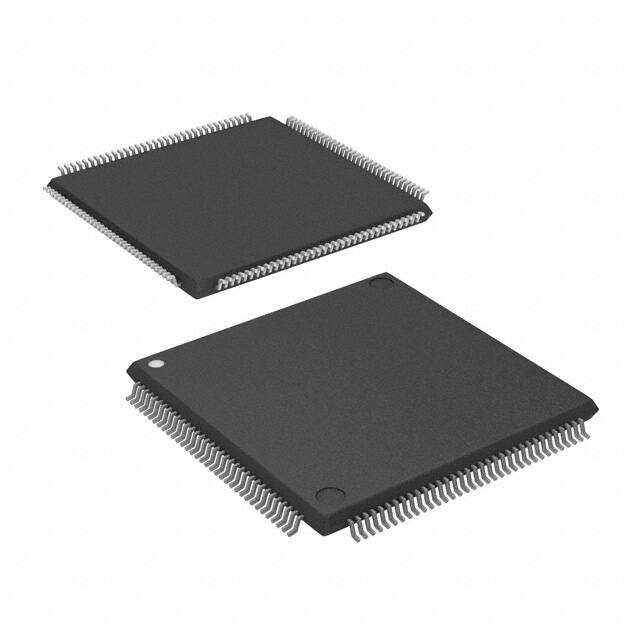


 工商网监
湘ICP备2023018690号
工商网监
湘ICP备2023018690号
