DKWF121 – WF121-A 802.11 B/G/N
MODULE EVALUATION BOARD
DATA SHEET
Thursday, 24 July 2014
Version 1.1
�Copyright © 2000-2014 Bluegiga Technologies
All rights reserved.
Bluegiga Technologies assumes no responsibility for any errors which may appear in this manual.
Furthermore, Bluegiga Technologies reserves the right to alter the hardware, software, and/or specifications
detailed here at any time without notice and does not make any commitment to update the information
contained here. Bluegiga’s products are not authorized for use as critical components in life support devices
or systems.
The WRAP, Bluegiga Access Server, Access Point and iWRAP are registered trademarks of Bluegiga
Technologies.
The Bluetooth trademark is owned by the Bluetooth SIG Inc., USA and is licensed to Bluegiga Technologies.
All other trademarks listed herein are owned by their respective owners.
Bluegiga Technologies Oy
�VERSION HISTORY
Version
Comment
1.0
First version
1.1
Updated Ethernet section, various small edits elsewhere
Bluegiga Technologies Oy
�TABLE OF CONTENTS
1
Product description ........................................................................................................................................5
2
Ordering Information......................................................................................................................................6
3
Board Description ..........................................................................................................................................7
3.1
Wi-Fi Module .........................................................................................................................................7
3.2
Crystals .................................................................................................................................................7
3.3
Configurable I/O Ports ..........................................................................................................................7
3.4
Bluetooth Coexistence ..........................................................................................................................8
3.5
LEDs and Buttons .................................................................................................................................8
3.6
USB Connections .................................................................................................................................9
3.7
Board Power ...................................................................................................................................... 10
3.8
Current Measurement Point J13 ........................................................................................................ 10
3.9
VDD_PA Selection Header J7 ........................................................................................................... 11
3.10
Ethernet ............................................................................................................................................. 11
3.11
Programming Connections ................................................................................................................ 12
3.12
Debug SPI Interface .......................................................................................................................... 12
3.13
Prototyping Area ................................................................................................................................ 12
4
Board layout ............................................................................................................................................... 13
5
Contact Information .................................................................................................................................... 14
Bluegiga Technologies Oy
�1
Product description
DESCRIPTION
DKWF121 is intended for evaluating the WF121
Wi-Fi module and as a basis for product
development. The board contains connectors
for easy development with a PC using the main
host connections, USB and UART through a
USB converter. Also present are headers for all
the GPIO pads connected around a prototyping
area for easy connection of pin headers with
custom pinouts, sensors etc.
Bluegiga WF121 is a stand-alone Wi-Fi module
providing fully integrated 2.4GHz 802.11 b/g/n
radio, TCP/IP stack and a 32-bit micro
controller (MCU)
platform
for
embedded
applications requiring simple, low-cost and lowpower wireless IP connectivity. WF121 also
provides flexible peripheral interfaces such as
SPI,
I2C,
ADC,
GPIO, Bluetooth coexistence and timers to connect various
peripheral interfaces directly to the WF121 WiFi module.
KEY FEATURES:
USB or UART host connection
USB converter for the UART
Can be powered through USB
Ethernet connection
Current measurement voltage output
Prototyping area
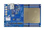
PHYSICAL OUTLOOK:
WF121 Wi-Fi module also allows end user
applications to be embedded onto the on-board
32-bit MCU using a simple Bluegiga
TM
BGScript scripting language and free-ofcharge development tools. This cuts out the
need of and additional MCU and enables end
users to develop smaller and lower cost Wi-Fi
devices. WF121 can also be used in modemlike mode in applications where the external
MCU is needed. The 802.11 access point and
HTTP server functionality is also included for
the easy configurations and direct connections
with phones, tablets and PC's.
With an integrated 802.11 radio, antenna, single
power supply, and CE, FCC and IC regulatory
certifications, WF121 provides a low-risk and
fast time-to-market for applications requiring WiFi connectivity.
Bluegiga Technologies Oy
�2
Ordering Information
Product code
Description
WF121-A-v2
WF121 Wi-Fi Module with internal chip antenna
WF121-E-v2
WF121 Wi-Fi Module with U.FL connector
DKWF121
WF121 development kit
Bluegiga Technologies Oy
Page 6 of 14
�3
3.1
Board Description
Wi-Fi Module
DKWF121 contains a WF121-A module variant, with an internal chip antenna.
3.2
Crystals
There are two crystals assembled on DKWF121, an 8MHz crystal for the WF121 CPU clocking and a
32.768kHz crystal for the CPU real time clock. The 8MHz crystal is needed when the WF121 USB connection
is used, otherwise it is not essential. The 32kHz crystal is also optional, and if extra GPIO are needed, the
0ohm resistors connecting the crystals to the module can be removed and moved to connect the pin headers
and prototyping area pads to the module pads. The pads are not connected to the pin headers by default as
crystal connections are always sensitive to noise.
3.3
Configurable I/O Ports
All the GPIO pads available on the WF121 are routed to pin headers for easy connection to other boards or a
logic analyzer. All the signals are also available on through-hole pads on the edges of the board prototyping
area for easy development prototyping.
Bluegiga Technologies Oy
Page 7 of 14
�The GPIO signals associated with the crystals are routed but not connected due to the presence of the
crystals, but if required the crystals can be removed and the associated 0ohm resistors moved to connect the
signals to the headers.
The signals shared for other functions like the ICSP programming interface, JTAG, UART’s and Ethernet
should not be driven by externally connected outputs when the mentioned functions are used to avoid
damage. The UART and Ethernet signals are disconnected when the associated on-board chips are disabled
with the on-board switches.
The USB pins are by default disconnected from the pin headers, but can be connected by adding two jumpers
to the specific header.
3.4
Bluetooth Coexistence
Industry standard 2-wire and 3-wire, as well as Unity-3, Unity-4, Unity-3e coexistence schemes are supported
and the associated signals are available. The PIO pads can be configured for these functions among others. A
U.FL connector is also present for antenna sharing using the module internal RF switch. As only 4 GPIO
signals can be used for coexistence, antenna sharing in practice requires the use of the CSR proprietary
Unity-3e scheme.
3.5
LEDs and Buttons
There are five LEDs and five pushbuttons on the DKWF121. One button is for module reset and one LED
indicates that the module has a power supply present, while the other four LEDs and buttons are available for
development purposes. The LEDs are buffered with MOSFETs and the buttons are open when unpressed,
allowing the connected GPIO lines to be used for other purposes without disconnecting the LEDs or buttons.
Bluegiga Technologies Oy
Page 8 of 14
�3.6
USB Connections
DKWF121 contains a microUSB connector for use with USB host connection, and a separate microUSB
connector with associated high speed USB-to-UART converter for UART host connection development with a
PC. The converter chip is a common dual-port FTDI type that will automatically register as a virtual serial port
in most operating systems with either inbuilt or automatically installed drivers.
Bluegiga Technologies Oy
Page 9 of 14
�The USB host connection includes a MOSFET power switch to allow host-mode operation with the DKWF121
feeding power to the external device. However, the current firmware does not support USB host mode.
3.7
SPI
No separate connectors for SPI host connections are provided as there is no standard connector or pinout,
but the signals are available on the pin headers and pads on the prototyping area edge for easy soldering of a
connector with a custom pinout.
3.8
Board Power
DKWF121 can be powered by several sources.
Both USB connectors can be used as the power supply input
A two-pin header
The signal pin headers and prototyping area connections have power connections
Note: if the on-board WF121 module does not contain firmware that operates the native USB connection, the
module cannot request an increase to the USB default current limit of 100mA. Although not all USB host
systems implement it, the USB specification states that the host should limit the current output to 100mA
unless an increase is requested, and using the module with high transmit duty cycles may cause the USB host
to go into current limit, possibly causing the module to crash. It is preferred to power the board through the
USB/UART-converter connector, the converter chip will automatically request for an increased current limit.
The board contains a switch mode converter that converts the 5V input to the 3.3V supply required by the
module. The converter is specified for output currents up to 600mA, allowing up to 200mA to be drawn for
powering customer applications.
The module operates down to 2.7V, but the current measure output and USB host functionality require a
regulated 5V input. The header and the USB connectors also have series schottky diodes, increasing the
minimum input voltage slightly. The 5V power connections in the prototyping area and the associated pin
headers do not have series diodes. The diodes allow connection of a USB host together with a separate
power supply without risk of damage.
3.9
Current Measurement Point J13
Header J13 contains a jumper that connects the switch mode regulator to the module 3.3V supply pads. The
jumper can be removed and the average current consumption of the module can be measured with a
multimeter or a series resistor can be inserted for measuring the momentary current consumption of the
module with an oscilloscope. Note that for average consumption measurement of anything else besides sleep
current a fast RMS multimeter is needed due to the pulsed nature of the consumption.
Removing the jumper also allows separation of the module supply lines from the regulator output, for example
when using an external regulator to supply the 3.3V voltage to the module is desired.
Bluegiga Technologies Oy
Page 10 of 14
�3.10
VDD_PA Selection Header J7
WF121 has two power supply inputs, VDD_3.3V (VDD_3.3V_MOD line on the schematic) and VDD_PA. The
VDD_3.3V pad supplies the internal processor and has a voltage range of 2.3V to 3.6V. The VDD_PA pad
supplies the internal WiFi-circuitry through a switch mode converter and the WiFi power amplifier directly. The
VDD_PA line can operate with input voltages between 2.7V and 5.5V, though the power consumption of the
power amplifier will grow in direct proportion to the input voltage. The separate supply however allows direct
connection to a lithium-ion battery, with just a small linear regulator limiting the supply voltage for the
processor side.
A jumper at header J7 usually connects VDD_PA to the board 3.3V switch mode converter output. The jumper
can be moved to the alternate position to supply the VDD_PA line directly from the 5V supply rail, for example
for connecting directly to a lithium battery either through the power input header or through the prototyping
area connections.
3.11
Ethernet
The board contains a 10/100Mbps Ethernet PHY with all the associated components, connected to the
module internal Ethernet MAC with an RMII interface. The PHY type is KSZ8081RNA or KSZ8031RNA,
depending on the production date. The KSZ8031 can be found on older boards and is now obsolete, but is
fully pin and function compatible with KSZ8081.
The PHY can be fully powered off and disconnected from the GPIO lines using switch SW1, allowing the
GPIO lines to be used for other functions. The PHY interrupt signal is available on a two-pin header marked
PHY IRQ, in case the interrupt functionality is required. By default it is not used.
The Ethernet connection is fully supported by the module firmware and can be used as a data endpoint,
allowing for example streaming data from Wi-Fi to the Ethernet.
Bluegiga Technologies Oy
Page 11 of 14
�3.12
Programming Connections
DKWF121 contains two connectors that allow direct programming of the WF121 internal processor. The
Microchip proprietary ICSP bus allows programming the full firmware image using a Microchip or third party
programming adapter. The pin header installed on the DKWF121 has a pinout suitable for use with the lowcost PicKit3 programming tool from Microchip. A JTAG connection is also available for basic boundary scans
and device programming. The JTAG does not support full device testing and debugging.
The primary means of uploading application data is through a host connection through the Bluegiga boot
loader. The programming connections should not be needed unless the internal boot loader is overwritten by
the application.
3.13
Debug SPI Interface
A header is provided for the module debug bus for certification RF testing. Access to internal settings and test
modes is available using a CSR compatible SPI adapter and UniTest-software.
For more information contact Bluegiga technical support.
3.14
Prototyping Area
DKWF121 contains an array of through plated holes with wide pads with a 2.54mm pitch for easy addition of
carrier boards, through-hole components and pin headers with a custom pinout. Also present is a smaller
array of pads with no holes using 1.27mm pitch for connecting SMD components like sensors, regulators etc
during system development.
All GPIO signals are routed to the prototyping area edges, though some of them are not by default connected
due to function multiplexing. See other chapters for detailed descriptions of these signals.
Also present on the pin headers and pads around the prototyping area are several supply voltage rails present
on the board. These can be used for powering external circuitry, or for powering the module with external
power sources. The uppermost and lowest rows of pads are connected to ground.
Bluegiga Technologies Oy
Page 12 of 14
�4
Board layout
Bluegiga Technologies Oy
Page 13 of 14
�5
Contact Information
Inquiries/ Support: www.bluegiga.com
Head office, Finland
Phone: +358-9-4355 060
Fax: +358-9-4355 0660
Bluegiga Technologies Oy
Sinikalliontie 5A, 5th floor
02630 Espoo, FINLAND
USA office
Phone: +1 770 291 2181
Fax: +1 770 291 2183
Bluegiga Technologies, Inc.
3235 Satellite Boulevard, Building 400, Suite 300,
Duluth, GA, 30096, USA
Hong Kong office
Phone: +852 3972 2186
Bluegiga Technologies Ltd.
Unit 10-18,
32/F, Tower 1, Millennium City 1,
388 Kwun Tong Road,
Kwun Tong,
Kowloon,
Hong Kong
Bluegiga Technologies Oy
Page 14 of 14
�


 工商网监
湘ICP备2023018690号
工商网监
湘ICP备2023018690号
