TS8
EMBER® EM3 X M ODULE TECHNICAL SPECIFICATION
Silicon Labs’ EM3x development kits contain various modules designed around the EM3x family of ICs. All of these
modules are designed and sold by Silicon Labs’ module partners Telegesis (UK) Limited and California Eastern
Laboratories (CEL). The module designs allow them to be integrated into any product without the need for RF
experience and expertise. Utilizing stacks such as Silicon Labs’ certified ZigBee network stack EmberZNet, these
modules enable a developer to add powerful wireless networking capability to products and quickly bring them to
market.
This document provides the technical specification of the EM3x modules on its Silicon Labs-specific carrier board.
For more information on the other Telegesis modules, contact Telegesis, Ltd directly at www.telegesis.com. For
more information on other CEL modules, contact CEL directly at meshconnect.cel.com.
New in This Revision
Added CEL CE compliance information.
Contents
1
EM3x Module Definitions................................................................................................................................. 2
2
EM3x Module Features ................................................................................................................................... 3
3
Performance Characteristics ........................................................................................................................... 3
4
EM3x Configurations ....................................................................................................................................... 5
5
Mechanical Details .......................................................................................................................................... 7
5.1
Rev 1.4
EM3x Module Interface Connector ........................................................................................................... 8
Copyright © 2015 by Silicon Laboratories
TS8
�TS8
1 EM3x Module Definitions
To accommodate the requirements of the different markets, Telegesis and CEL have developed a series of pincompatible modules based on the Ember EM341, EM346, EM357, and EM3588 chipsets. Table 1 defines the
Telegesis, CEL, and Silicon Labs part numbers for each module as well as describes the differences (Power
Amplifier (PA), Low Noise Amplifier (LNA), and RF connection) between each module.
Table 1. Silicon Labs and Module Partner Part Numbers
RF Connection
PA /
LNA?
(Long
Range)
ZICM341SP0-1
Antenna
No
ZICM341SP0-1C
Connector
No
ZICM346SP0-1
Antenna
No
ZICM346SP0-1C
Connector
No
ETRX357
SMT Antenna
No
ETRX357HR
Mini-RF Connector
No
ETRX357HR-LRS
Mini-RF Connector
Yes
Telegesis
ETRX357-LRS
SMT Antenna
Yes
CEL
ZICM357SP0-1
SMT Antenna
No
EM357
CEL
ZICM357SP0-1C
Mini-RF Connector
No
EM357
CEL
ZICM357SP2-1C
Mini-RF Connector
Yes
EM357-MOD-LR-ANT-C
EM357
CEL
ZICM357SP2-1
SMT Antenna
Yes
EM3588-M-AN-C
EM3588
CEL
ZICM3588SP0-1
SMT Antenna
No
110-0735-000
EM3588-MOD-RF-C
EM3588
CEL
ZICM3588SP0-1C
Mini-RF Connector
No
110-0736-000
EM3588-MLR-RF-C
EM3588
CEL
ZICM3588SP2-1C
Mini-RF Connector
Yes
110-0737-000
EM3588-MLR-AN-C
EM3588
CEL
ZICM3588SP2-1
SMT Antenna
Yes
Silicon Labs
P/N
Silicon Labs Orderable
Part Number (OPN)
EM3x
IC
Module
Partner
110-0740-000
EM341-MOD-ANT-C
EM341
CEL
110-0741-000
EM341-MOD-RF-C
EM341
CEL
110-0742-000
EM346-MOD-ANT-C
EM346
CEL
110-0743-000
EM346-MOD-RF-C
EM346
CEL
110-0720-000
EM357-MOD-ANT-T
EM357
Telegesis
110-0721-000
EM357-MOD-RF-T
EM357
Telegesis
110-0722-000
EM357-MOD-LR-RF-T
EM357
Telegesis
110-0723-000
EM357-MOD-LR-ANT-T
EM357
110-0730-000
EM357-MOD-ANT-C
EM357
110-0731-000
EM357-MOD-RF-C
110-0732-000
EM357-MOD-LR-RF-C
110-0733-000
110-0734-000
Module Partner P/N
(Module only)
All of these modules are available from Telegesis and CEL. Silicon Labs provides the CEL EM357 and EM3588
module types with the EM35x Development Kit (part number EM35X-DEV) and the EM341 and EM346 modules
with the EM34x Development Kit (part number EM34X-DEV).
For modules whose RF connection is a mini-RF connector, an RF adapter cable (Tyco/Amp part number 20324401) can be used to interface the module to external test equipment. One of these RF adapter cables is included with
the development kits.
To connect to the EM35x breakout board (Silicon Labs P/N: 130-0680-000), each module shown in Table 1 is
soldered to a small carrier board. The carrier board connector is discussed in section 5.1, EM3x Module Interface
Connector.
2
Rev. 1.4
�TS8
2 EM3x Module Features
Module features:
•
•
•
•
•
•
•
•
Small form factor, SMT module (25 mm x 19 mm)
Side castellation for easy soldering and inspection
Industry standard JTAG Programming and real-time network level debugging via the Packet Trace Port.
Wide supply voltage range (2.1 to 3.6 V)
Low sleep current (< 1 µA for EM35x and EM34x, < 2 µA for EM3588)
Access to all EM3x GPIO from the System-on-Chip (SoC)
Access to either a U.FL RF Connector or a SMT antenna allows flexibility in antenna selection process
FCC compliance
Telegesis:
FCC ID: S4GEM35XA
CEL:
•
FCC ID: W7Z-ZICM357SPO
FCC ID: W7Z-ZICM357SP2
CE compliance
Telegesis:
Radio: EN300 328 v1.7.1
EMC: EN301 489-17 v2.1.1
Safety: EN60950-1
CEL
•
Radio: EN 300 328 V1.8.1 (2006 ‐ 2012)
EMC: EN 301 489‐1 V1.8.1, V1.9.1
EN 301 489‐17 V2.2.1
Long Range versions with a link budget of up to 124 dB
Module with carrier board features:
•
•
•
Access to the Packet Trace Port connector (allows for direct connection to the Ember Debug Adapter
(ISA3) for programming and debugging)
Two debug LEDs
Access to all EM3x GPIO through a robust 0.05” pitch connector
3 Performance Characteristics
This section describes the characteristics of the module with carrier board. For more information on the EM35x and
EM34x SoC performance, refer to the EM35x, EM358x, EM341 and EM346 data sheets.
Unless specified, the data within each of the tables was gathered at room temperature (25 °C) and 3.0 V source
potential. Table 2 summarizes the recommended operating conditions for the modules.
Table 2. Recommended Operating Conditions for the EM3x Module
Parameter
Min
Typ
Max
Unit
VDD supply
2.1
—
3.6
V
RF Input Frequency
2405
—
2480
MHz
RF Input Power (at RF Port)
—
—
0
dBm
Operating Temperature Range
-40
—
85
°C
Rev. 1.4
3
�TS8
Table 3 summarizes the DC characteristics at 25 °C and VDD of 3 V of the EM3x Module.
Table 3. DC Characteristics of the EM3x Module
Parameter
Min
Typ
Max
Unit
VDD supply
2.1
—
3.6
V
Sleep Current (RC oscillator)
—
0.4
—
µA
TX, Normal Mode, +3 dBm
—
31
—
mA
TX, Boost Mode, +8 dBm
—
39
—
mA
TX, Normal Mode, 0 dBm
—
28.5
—
RX, Normal Mode
—
26
—
mA
RX, Boost Mode
Active Current (TX)
Active Current (RX)
—
27
—
mA
Wake Time from Deep Sleep
—
100
—
us
Shutdown Time
—
5
—
us
Table 4 summarizes the digital I/Os at VCC = 3 V and 25 °C of the EM3x Module.
Table 4. Digital I/O Characteristics of the EM3x Module
Parameter
Min
Typ
Max
Unit
Schmitt threshold (high to low)
0.42 x VDD
—
0.5 x VDD
V
Schmitt threshold (low to high)
0.62 x VDD
—
0.8 x VDD
V
Logic Low
—
—
-0.5
µA
Logic High
—
—
0.5
µA
Output Voltage
—
—
—
Logic Low
0
—
0.18 x VDD
V
Logic High
0.82 x VDD
—
VDD
V
Source, Standard Pad
—
—
4
mA
Sink, Standard Pad
—
—
4
mA
Source, High Current Pad
—
—
8
mA
Sink, High Current Pad
—
—
8
mA
Total Output Current
—
—
40
mA
Input Logic Threshold
Input Current
Output Current
4
Rev. 1.4
�TS8
Table 5 summarizes the RF parameters of the EM3x Module.
Table 5. RF Characteristics of the EM3x Module
Parameter
Min
Typ
Max
Unit
Frequency Range
2405
—
2480
MHz
Channel Spacing
—
5
—
MHz
Normal Mode
—
-100
-94
dBm
Boost Mode
—
-101
-95
dBm
—
35
—
dB
RX Sensitivity (1% PER, 20-byte packet)
Adjacent Channel Rejection
High Side
Low Side
—
35
—
dB
2nd High Side
—
43
—
dB
2nd Low Side
—
43
—
dB
All other channels
—
40
—
dB
Boost Mode
—
8
—
dBm
Normal Mode
—
3
—
dBm
—
5
15
%
Relative
-20
—
—
dB
Absolute
-30
—
—
dBm
TX Power (Maximum)
Error Vector Magnitude (Offset EVM) (per IEEE 802.15.4-2003)
PSD (3.5 MHz from carrier)
4 EM3x Configurations
The IC on the EM3x Module can be set to different RF frequency channels as well as different power levels. When
using the nodetest application on the module, the frequency channels and output power levels can be configured
through a command line interface (CLI).
In order to configure the output power, the setTXPower command can be used. Table 6 demonstrates the
setTXPower command and the expected power output. Note that these are the typical expected power output
levels based on the performance of the EM3x IC and actual results are dependent on the module provider design
implementation.
Note: Table 6 refers to the non-PA versions of the modules. For the version with a PA, the output power should be
set to -5 dBm in order to achieve +20 dBm output power.
Table 6: List of TX output powers when using SetTxPower
SetTxPower
[signed hexadecimal]
Output Power
(dBm)
SetTxPower 9
+3
SetTxPower 8
+8
SetTxPower 7
+7
SetTxPower 6
+6
SetTxPower 5
+5
Rev. 1.4
5
�TS8
SetTxPower
[signed hexadecimal]
6
Output Power
(dBm)
SetTxPower 4
+4
SetTxPower 3
+3
SetTxPower 2
+2
SetTxPower 1
+1
SetTxPower 0
0
SetTxPower -1
-1
SetTxPower -2
-2
SetTxPower -3
-3
SetTxPower -4
-4
SetTxPower -5
-5
SetTxPower -6
-6
SetTxPower -7
-7
SetTxPower -8
-8
SetTxPower -9
-9
SetTxPower –a
-9
SetTxPower –b
-11
SetTxPower –c
-12
SetTxPower –d
-12
SetTxPower –e
-14
SetTxPower –f
-14
SetTxPower -10
-14
SetTxPower -11
-17
SetTxPower -12
-17
SetTxPower -13
-17
SetTxPower -14
-20
SetTxPower -15
-20
SetTxPower -16
-20
SetTxPower -17
-20
Rev. 1.4
�TS8
To change the channel, the setChannel command can be used (assuming nodetest application is on the device).
Table 7 lists the valid parameters to be used with setChannel command.
Table 7: List of setChannel values for EM3x
setChannel
(decimal)
Center
Frequency (GHz)
radioChannel
(decimal)
Center
Frequency (GHz)
11
2.405
19
2.445
12
2.410
20
2.450
13
2.415
21
2.455
14
2.420
22
2.460
15
2.425
23
2.465
16
2.430
24
2.470
17
2.435
25
2.475
18
2.440
26
2.480
5 Mechanical Details
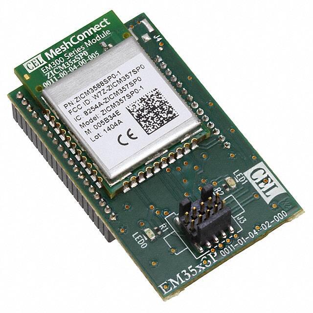
Figure 1 illustrates the ZICM35x Module carrier board from CEL, while Figure 2 illustrates the ETRX35x Module
from Telegesis on a carrier board.
Figure 1. CEL ZICM35x Module Carrier Board
Rev. 1.4
7
�TS8
LED2
20
32.768kHz
33
ETRX35x Module
22 mm
Packet
Trace Port
19
1
LED1
37.5 mm
Figure 2. Telegesis ETRX35x Module with Carrier Board
5.1
EM3x Module Interface Connector
EM35x_PB5
EM35x_PB6
EM35x_PB7
EM35x_PC0
EM35x_PC1
EM35x_PB0
EM35x_PC4
EM35x_PC3
EM35x_PC2
JCLK
GND
29
28
27
26
25
24
23
22
21
20
10
11
12
13
14
15
16
17
18
19
EM35x_PA2
EM35x_PA3
GND
EM35x_PA4
EM35x_PA5
EM35x_PA6
EM35x_PB1
EM35x_PB2
GND
EM35x_PB4
EM35x_PA1
8
EM35x_PA0
GND
7
nRESET
30
VDD_3V_MOD
31
6
EM35x_PB3
9
GND
33
32
4
5
EM35x_PA7
3
EM35x_PC6
EM35x_PC7
1
2
GND
EM35x_PC5
Two single-row, 0.05” pitch, connectors make up the EM3x module interface to the EM35x breakout board. In
addition, two single-row, guide connectors on the EM35x breakout board assist with connecting the EM3x module
to the breakout board. The board-to-board connector scheme allows access to all EM3x GPIO as well as nRESET
and the JCLK signals. The connector is illustrated in Figure 3, while the connector dimensions are listed in Figure 4.
Figure 3. Board-to-board connector for the EM3x module (top view)
8
Rev. 1.4
�TS8
Figure 4. Board-to-Board Connector Dimensions for the EM3x Module (top view)
Table 8 describes the pinout and signal names on the connector.
For more information on the alternate functions of the GPIO connector, refer to the EM35x Data Sheet.
Table 8. Pinout and Signal Names of the Interface Connector
Signal name
Direction1
Description
1
GND
Power
Ground Connection
2
PC5
I/O
EM3x GPIO
3
PC6
I/O
EM3x GPIO
4
PC7
I/O
EM3x GPIO
5
PA7
I/O
EM3x GPIO
6
PB3
I/O
EM3x GPIO
7
nRESET
I/O
Active low chip reset (internal pull-up on EM3x)
8
PB4
I/O
EM3x GPIO
9
PA0
I/O
EM3x GPIO
Pin #
10
PA1
I/O
EM3x GPIO
11
PA2
I/O
EM3x GPIO
12
PA3
I/O
EM3x GPIO
13
GND
Power
Ground Connection
14
PA4
I/O
EM3x GPIO
15
PA5
I/O
EM3x GPIO
16
PA6
I/O
EM3x GPIO (NC on EM346 module)
17
PB1
I/O
EM3x GPIO
18
PB2
I/O
EM3x GPIO
19
GND
Power
Ground connection
20
GND
Power
Ground connection
21
JCLK
Input
JTAG interface, serial clock
22
PC2
I/O
EM3x GPIO
23
PC3
I/O
EM3x GPIO
Rev. 1.4
9
�TS8
Signal name
Direction1
Description
24
PC4
I/O
EM3x GPIO
25
PB0
I/O
EM3x GPIO
26
PC1
I/O
EM3x GPIO
27
PC0
I/O
EM3x GPIO
28
PB7
I/O
EM3x GPIO (NC on EM346 module)
29
PB6
I/O
EM3x GPIO (NC on EM346 module)
30
PB5
I/O
EM3x GPIO (NC on EM346 module)
31
GND
Power
Ground connection
32
VDD
Power
2.1 to 3.6 V Module Power Domain
33
GND
Power
Ground connection
Pin #
1
with respect to the EM3x Module
10
Rev. 1.4
�TS8
CONTACT INFORMATION
Silicon Laboratories Inc.
400 West Cesar Chavez
Austin, TX 78701
Tel: 1+(512) 416-8500
Fax: 1+(512) 416-9669
Toll Free: 1+(877) 444-3032
For additional information please visit the Silicon Labs Technical Support page:
http://www.silabs.com/support/Pages/default.aspx
Patent Notice
Silicon Labs invests in research and development to help our customers differentiate in the market with innovative low-power, small size,
analog-intensive mixed-signal solutions. Silicon Labs' extensive patent portfolio is a testament to our unique approach and world-class
engineering team.
The information in this document is believed to be accurate in all respects at the time of publication but is subject to change without notice.
Silicon Laboratories assumes no responsibility for errors and omissions, and disclaims responsibility for any consequences resulting from the
use of information included herein. Additionally, Silicon Laboratories assumes no responsibility for the functioning of undescribed features or
parameters. Silicon Laboratories reserves the right to make changes without further notice. Silicon Laboratories makes no warranty,
representation or guarantee regarding the suitability of its products for any particular purpose, nor does Silicon Laboratories assume any liability
arising out of the application or use of any product or circuit, and specifically disclaims any and all liability, including without limitation
consequential or incidental damages. Silicon Laboratories products are not designed, intended, or authorized for use in applications intended to
support or sustain life, or for any other application in which the failure of the Silicon Laboratories product could create a situation where personal
injury or death may occur. Should Buyer purchase or use Silicon Laboratories products for any such unintended or unauthorized application,
Buyer shall indemnify and hold Silicon Laboratories harmless against all claims and damages.
Silicon Laboratories, Silicon Labs, and Ember are registered trademarks of Silicon Laboratories Inc.
Other products or brandnames mentioned herein are trademarks or registered trademarks of their respective holders.
Rev. 1.4
11
�


 工商网监
湘ICP备2023018690号
工商网监
湘ICP备2023018690号
