Si102x/3x
Ultra Low Power, 64/32 kB, 10-Bit ADC
MCU with Integrated 240–960 MHz EZRadioPRO® Transceiver
-
-
RF power consumption
18.5 mA receive
18 mA @ +1 dBm transmit
30 mA @ +13 dBm transmit
85 mA @ +20 dBm transmit
Data rate = 0.123 to 256 kbps
Auto-frequency calibration (AFC)
Antenna diversity and transmit/receive switch control
Programmable packet handler
TX and RX 64-byte FIFOs
Frequency hopping capability
On-chip crystal tuning
130 µA/MHz IBAT; dc-dc enabled
110 nA sleep current with data retention; POR monitor enabled
400 nA sleep current with smaRTClock (internal LFO)
700 nA sleep current with smaRTClock (external XTAL)
2 µs wake-up from any sleep mode
12-Bit; 16 Ch. Analog-to-Digital Converter
-
High-Speed 8051 µC Core
-
Memory
-
Two Low Current Comparators
-
Digital Peripherals
-
-
-
Up to ±500 µA; source and sink capability
Enhanced resolution via PWM interpolation
Integrated LCD Controller (Si102x Only)
-
EZRadioPRO Transceiver
-
-
Precision internal oscillators: 24.5 MHz with ±2% accuracy supports UART operation; spread-spectrum mode for reduced EMI
Low power internal oscillator: 20 MHz
External oscillator: Crystal, RC, C, CMOS clock
smaRTClock oscillator: 32.768 kHz crystal or 16.4 kHz internal
LFO with three independent alarms
fo
r
-
Clock Sources
DC-DC buck converter allows dynamic voltage scaling for
maximum efficiency (250 mW output)
Sleep-mode pulse accumulator with programmable switch
de-bounce and pull-up control interfaces directly to metering sensor
Dedicated Packet Processing Engine (DPPE) includes hardware
AES, DMA, CRC, and encoding blocks for acceleration of wireless
protocols
Manchester and 3 out of 6 encoder hardware for power efficient
implementation of the wireless M-bus specification
®
-
On-Chip Debug
m
en
de
d
-
53 port I/O; All 5 V tolerant with high sink
current and programmable drive strength
Hardware SMBus™ (I2C™ compatible), 2 x SPI™, and UART
serial ports available concurrently
Four general-purpose 16-bit counter/timers
Programmable 16-bit counter/timer array with six capture/compare
modules and watchdog timer
-
Supports up to 128 segments (32x4)
Integrated charge pump for contrast control
Metering-Specific Peripherals
-
Up to 128 kB Flash; In-system programmable; Full read/write/erase
functionality over the entire supply range
Up to 8 kB internal data RAM
-
Programmable hysteresis and response time
Configurable as interrupt or reset source
Internal 6-Bit Current Reference
-
Pipelined instruction architecture; executes 70% of instructions in 1
or 2 system clocks
D
-
Up to 75 ksps 12-bit mode or 300 ksps 10-bit mode
External pin or internal VREF (no external capacitor required)
On-chip PGA allows measuring voltages up to twice the reference
voltage
Autonomous burst mode with 16-bit automatic averaging
accumulator
Integrated temperature sensor
N
ew
-
es
ig
ns
Ultra Low Power at 3.6V
-
om
Reset
Debug /
Programming
Hardware
ec
R
N
ot
VBATDC
IND
CAP
SMBus
Analog
Power
CRC
Engine
SPI 0
Digital
Power
AES
Engine
DC/DC Buck
Converter
SYSCLK
Precision
24.5 MHz
Oscillator
LCD Charge
Pump
XTAL1
XTAL2
GND
VREG
XTAL3
XTAL4
Low Power
20 MHz
Oscillator
External
Oscillator
Circuit
Enhanced
smaRTClock
Oscillator
System Clock
Configuration
Rev. 1.0 2/13
Priority
Crossbar
Decoder
PCA/
WDT
DMA
Encoder
GNDDC
Timers
0/1/2/3
256 Byte SRAM
VBAT
VDC
UART
8192/4096 Byte XRAM
C2D
VDD
Digital Peripherals
128/64/32/16 kByte
ISP Flash Program
Memory
Wake
–85 pin LGA (6 x 8 mm)
Port I/O Configuration
CIP-51 8051
Controller Core
Power On
Reset/PMU
VBAT
-
On-chip debug circuitry facilitates full-speed, non-intrusive, in-system debug (no emulator required)
Provides 4 breakpoints, single stepping
Packages
Frequency range = 240–960 MHz
Sensitivity = –121 dBm
FSK, GFSK, and OOK modulation
Max output power = +20 dBm or +13 dBm
C2CK/RST
-
Port 0-1
Drivers
16
Port 2
Drivers
4
Port 3-6
Drivers
32
Port 7
Driver
P2.4...P2.7
P3.0...P6.7
P7.0/C2D
RF XCVR
(240-960 MHz,
+20/+13 dBm)
Crossbar Control
PA
VCO
LCD (4x32)
SFR
Bus
P0.0...P1.7
TX
EMIF
AGC
RXp
RXn
Pulse Counter
LNA
EZRadioPro SPI 1
Mixer
PGA
Analog Peripherals
Internal
External
VREF
VREF
A
M
U
X
12-bit
75ksps
ADC
ADC
Digital
Modem
VDD
VREF
Temp
Sensor
Delta
Sigma
Modulator
Digital
Logic
GND
CP0, CP0A
CP1, CP1A
+
-
+
-
30 MHz
3
SDN
nIRQ
GPIOx
XOUT
XIN
Comparators
Copyright © 2013 by Silicon Laboratories
Si102x/3x
�2
Rev. 1.0
N
ot
m
en
de
d
om
ec
R
fo
r
N
ew
es
ig
ns
D
�Si102x/3x
Table of Contents
N
ot
R
ec
om
m
en
de
d
fo
r
N
ew
D
es
ig
ns
1. System Overview ..................................................................................................... 25
1.1. Typical Connection Diagram ............................................................................. 28
1.2. CIP-51™ Microcontroller Core .......................................................................... 29
1.2.1. Fully 8051 Compatible .............................................................................. 29
1.2.2. Improved Throughput................................................................................ 29
1.2.3. Additional Features ................................................................................... 29
1.3. Port Input/Output ............................................................................................... 30
1.4. Serial Ports ........................................................................................................ 31
1.5. Programmable Counter Array............................................................................ 31
1.6. SAR ADC with 16-bit Auto-Averaging Accumulator and Autonomous Low Power
Burst Mode.......................................................................................................... 32
1.7. Programmable Current Reference (IREF0)....................................................... 33
1.8. Comparators...................................................................................................... 33
2. Ordering Information ............................................................................................... 35
3. Pinout and Package Definitions ............................................................................. 36
3.1. LGA-85 Package Specifications ........................................................................ 45
3.1.1. Package Drawing ...................................................................................... 45
3.1.2. Land Pattern.............................................................................................. 47
4. Electrical Characteristics ........................................................................................ 48
4.1. Absolute Maximum Specifications..................................................................... 48
4.2. MCU Electrical Characteristics .......................................................................... 49
4.3. EZRadioPRO® Peripheral Electrical Characteristics......................................... 70
5. SAR ADC with 16-bit Auto-Averaging Accumulator and Autonomous Low Power
Burst Mode ................................................................................................................... 77
5.1. Output Code Formatting .................................................................................... 77
5.2. Modes of Operation ........................................................................................... 79
5.2.1. Starting a Conversion................................................................................ 79
5.2.2. Tracking Modes......................................................................................... 79
5.2.3. Burst Mode................................................................................................ 81
5.2.4. Settling Time Requirements...................................................................... 82
5.2.5. Gain Setting .............................................................................................. 82
5.3. 8-Bit Mode ......................................................................................................... 83
5.4. 12-Bit Mode ....................................................................................................... 83
5.5. Low Power Mode............................................................................................... 84
5.6. Programmable Window Detector....................................................................... 90
5.6.1. Window Detector In Single-Ended Mode .................................................. 92
5.6.2. ADC0 Specifications ................................................................................. 93
5.7. ADC0 Analog Multiplexer .................................................................................. 94
5.8. Temperature Sensor.......................................................................................... 96
5.8.1. Calibration ................................................................................................. 96
5.9. Voltage and Ground Reference Options ........................................................... 99
5.10. External Voltage Reference........................................................................... 100
5.11. Internal Voltage Reference............................................................................ 100
Rev. 1.0
3
�Si102x/3x
N
ot
R
ec
om
m
en
de
d
fo
r
N
ew
D
es
ig
ns
5.12. Analog Ground Reference............................................................................. 100
5.13. Temperature Sensor Enable ......................................................................... 100
5.14. Voltage Reference Electrical Specifications .................................................. 101
6. Programmable Current Reference (IREF0).......................................................... 102
6.1. PWM Enhanced Mode..................................................................................... 102
6.2. IREF0 Specifications ....................................................................................... 103
7. Comparators........................................................................................................... 104
7.1. Comparator Inputs........................................................................................... 104
7.2. Comparator Outputs ........................................................................................ 105
7.3. Comparator Response Time ........................................................................... 106
7.4. Comparator Hysterisis ..................................................................................... 106
7.5. Comparator Register Descriptions .................................................................. 107
7.6. Comparator0 and Comparator1 Analog Multiplexers ...................................... 111
8. CIP-51 Microcontroller........................................................................................... 114
8.1. Instruction Set.................................................................................................. 115
8.1.1. Instruction and CPU Timing .................................................................... 115
8.2. CIP-51 Register Descriptions .......................................................................... 120
9. Memory Organization ............................................................................................ 123
9.1. Program Memory............................................................................................. 123
9.1.1. MOVX Instruction and Program Memory ................................................ 126
9.2. Data Memory ................................................................................................... 126
9.2.1. Internal RAM ........................................................................................... 127
9.2.2. External RAM .......................................................................................... 127
10. External Data Memory Interface and On-Chip XRAM ....................................... 128
10.1. Accessing XRAM........................................................................................... 128
10.1.1. 16-Bit MOVX Example .......................................................................... 128
10.1.2. 8-Bit MOVX Example ............................................................................ 128
10.2. Configuring the External Memory Interface (EMIF) ....................................... 129
10.3. Port Configuration.......................................................................................... 129
10.4. Multiplexed and Non-Multiplexed Selection................................................... 133
10.4.1. Multiplexed Configuration...................................................................... 133
10.4.2. Non-Multiplexed Configuration.............................................................. 133
10.5. Memory Mode Selection................................................................................ 134
10.5.1. Internal XRAM Only .............................................................................. 135
10.5.2. Split Mode without Bank Select............................................................. 135
10.5.3. Split Mode with Bank Select.................................................................. 135
10.5.4. External Only......................................................................................... 135
10.6. Timing .......................................................................................................... 136
10.6.1. Non-Multiplexed Mode .......................................................................... 138
10.6.2. Multiplexed Mode .................................................................................. 141
11. Direct Memory Access (DMA0)........................................................................... 145
11.1. DMA0 Architecture ........................................................................................ 146
11.2. DMA0 Arbitration ........................................................................................... 147
11.2.1. DMA0 Memory Access Arbitration ........................................................ 147
11.2.2. DMA0 Channel Arbitration .................................................................... 147
4
Rev. 1.0
�Si102x/3x
N
ot
R
ec
om
m
en
de
d
fo
r
N
ew
D
es
ig
ns
11.3. DMA0 Operation in Low Power Modes ......................................................... 147
11.4. Transfer Configuration................................................................................... 148
12. Cyclic Redundancy Check Unit (CRC0)............................................................. 159
12.1. 16-bit CRC Algorithm..................................................................................... 159
12.3. Preparing for a CRC Calculation ................................................................... 162
12.4. Performing a CRC Calculation ...................................................................... 162
12.5. Accessing the CRC0 Result .......................................................................... 162
12.6. CRC0 Bit Reverse Feature............................................................................ 166
13. DMA-Enabled Cyclic Redundancy Check Module (CRC1)............................... 167
13.1. Polynomial Specification................................................................................ 167
13.2. Endianness.................................................................................................... 168
13.3. CRC Seed Value ........................................................................................... 169
13.4. Inverting the Final Value................................................................................ 169
13.5. Flipping the Final Value ................................................................................. 169
13.6. Using CRC1 with SFR Access ...................................................................... 170
13.7. Using the CRC1 module with the DMA ......................................................... 170
14. Advanced Encryption Standard (AES) Peripheral ............................................ 174
14.1. Hardware Description .................................................................................... 175
14.1.1. AES Encryption/Decryption Core .......................................................... 176
14.1.2. Data SFRs............................................................................................. 176
14.1.3. Configuration SFRs............................................................................... 177
14.1.4. Input Multiplexer.................................................................................... 177
14.1.5. Output Multiplexer ................................................................................. 177
14.1.6. Internal State Machine .......................................................................... 177
14.2. Key Inversion................................................................................................. 178
14.2.1. Key Inversion using DMA...................................................................... 179
14.2.2. Key Inversion using SFRs..................................................................... 180
14.2.3. Extended Key Output Byte Order.......................................................... 181
14.2.4. Using the DMA to unwrap the extended Key ........................................ 182
14.3. AES Block Cipher .......................................................................................... 183
14.4. AES Block Cipher Data Flow......................................................................... 184
14.4.1. AES Block Cipher Encryption using DMA ............................................. 185
14.4.2. AES Block Cipher Encryption using SFRs ............................................ 186
14.5. AES Block Cipher Decryption........................................................................ 187
14.5.1. AES Block Cipher Decryption using DMA............................................. 187
14.5.2. AES Block Cipher Decryption using SFRs............................................ 188
14.6. Block Cipher Modes ...................................................................................... 189
14.6.1. Cipher Block Chaining Mode................................................................. 189
14.6.2. CBC Encryption Initialization Vector Location....................................... 191
14.6.3. CBC Encryption using DMA .................................................................. 191
14.6.4. CBC Decryption .................................................................................... 194
14.6.5. Counter Mode ....................................................................................... 197
14.6.6. CTR Encryption using DMA .................................................................. 199
15. Encoder/Decoder ................................................................................................. 206
15.1. Manchester Encoding.................................................................................... 207
Rev. 1.0
5
�Si102x/3x
N
ot
R
ec
om
m
en
de
d
fo
r
N
ew
D
es
ig
ns
15.2. Manchester Decoding.................................................................................... 208
15.3. Three-out-of-Six Encoding............................................................................ 209
15.4. Three-out-of-Six Decoding ............................................................................ 210
15.5. Encoding/Decoding with SFR Access ........................................................... 211
15.6. Decoder Error Interrupt.................................................................................. 211
15.7. Using the ENC0 module with the DMA.......................................................... 212
16. Special Function Registers................................................................................. 215
16.1. SFR Paging ................................................................................................... 215
16.2. Interrupts and SFR Paging ............................................................................ 215
17. Interrupt Handler.................................................................................................. 231
17.1. Enabling Interrupt Sources ............................................................................ 231
17.2. MCU Interrupt Sources and Vectors.............................................................. 231
17.3. Interrupt Priorities .......................................................................................... 232
17.4. Interrupt Latency............................................................................................ 232
17.5. Interrupt Register Descriptions ...................................................................... 234
17.6. External Interrupts INT0 and INT1................................................................. 241
18. Flash Memory....................................................................................................... 243
18.1. Programming the Flash Memory ................................................................... 243
18.1.1. Flash Lock and Key Functions .............................................................. 243
18.1.2. Flash Erase Procedure ......................................................................... 243
18.1.3. Flash Write Procedure .......................................................................... 244
18.1.4. Flash Write Optimization ....................................................................... 245
18.2. Non-volatile Data Storage ............................................................................. 246
18.3. Security Options ............................................................................................ 246
18.4. Determining the Device Part Number at Run Time ....................................... 248
18.5. Flash Write and Erase Guidelines ................................................................. 249
18.5.1. VDD Maintenance and the VDD Monitor .............................................. 249
18.5.2. PSWE Maintenance .............................................................................. 251
18.5.3. System Clock ........................................................................................ 251
18.6. Minimizing Flash Read Current ..................................................................... 252
19. Power Management ............................................................................................. 257
19.1. Normal Mode ................................................................................................. 258
19.2. Idle Mode....................................................................................................... 258
19.3. Stop Mode ..................................................................................................... 259
19.4. Low Power Idle Mode .................................................................................... 259
19.5. Suspend Mode .............................................................................................. 263
19.6. Sleep Mode ................................................................................................... 263
19.7. Configuring Wakeup Sources........................................................................ 264
19.8. Determining the Event that Caused the Last Wakeup................................... 264
19.9. Power Management Specifications ............................................................... 268
20. On-Chip DC-DC Buck Converter (DC0).............................................................. 269
20.1. Startup Behavior............................................................................................ 270
20.4. Optimizing Board Layout ............................................................................... 271
20.5. Selecting the Optimum Switch Size............................................................... 271
20.6. DC-DC Converter Clocking Options .......................................................... 271
6
Rev. 1.0
�Si102x/3x
N
ot
R
ec
om
m
en
de
d
fo
r
N
ew
D
es
ig
ns
20.7. Bypass Mode................................................................................................. 272
20.8. DC-DC Converter Register Descriptions ....................................................... 272
20.9. DC-DC Converter Specifications ................................................................... 276
21. Voltage Regulator (VREG0)................................................................................. 277
21.1. Voltage Regulator Electrical Specifications ................................................... 277
22. Reset Sources ...................................................................................................... 278
22.1. Power-On Reset ............................................................................................ 279
22.2. Power-Fail Reset ........................................................................................... 280
22.3. External Reset ............................................................................................... 283
22.4. Missing Clock Detector Reset ....................................................................... 283
22.5. Comparator0 Reset ....................................................................................... 283
22.6. PCA Watchdog Timer Reset ......................................................................... 283
22.7. Flash Error Reset .......................................................................................... 284
22.8. SmaRTClock (Real Time Clock) Reset ......................................................... 284
22.9. Software Reset .............................................................................................. 284
23. Clocking Sources................................................................................................. 286
23.1. Programmable Precision Internal Oscillator .................................................. 287
23.2. Low Power Internal Oscillator........................................................................ 287
23.3. External Oscillator Drive Circuit..................................................................... 287
23.3.1. External Crystal Mode........................................................................... 287
23.3.2. External RC Mode................................................................................. 289
23.3.3. External Capacitor Mode....................................................................... 290
23.3.4. External CMOS Clock Mode ................................................................. 290
23.4. Special Function Registers for Selecting and Configuring the System Clock 291
24. SmaRTClock (Real Time Clock).......................................................................... 295
24.1. SmaRTClock Interface .................................................................................. 296
24.1.1. SmaRTClock Lock and Key Functions.................................................. 297
24.1.2. Using RTC0ADR and RTC0DAT to Access SmaRTClock Internal Registers
..................................................................................................... 297
24.1.3. SmaRTClock Interface Autoread Feature ............................................. 297
24.1.4. RTC0ADR Autoincrement Feature........................................................ 297
24.2. SmaRTClock Clocking Sources .................................................................... 300
24.2.1. Using the SmaRTClock Oscillator with a Crystal or External CMOS Clock
..................................................................................................... 300
24.2.2. Using the SmaRTClock Oscillator in Self-Oscillate Mode..................... 301
24.2.3. Using the Low Frequency Oscillator (LFO) ........................................... 301
24.2.4. Programmable Load Capacitance......................................................... 301
24.2.5. Automatic Gain Control (Crystal Mode Only) and SmaRTClock Bias
Doubling
..................................................................................................... 302
24.2.6. Missing SmaRTClock Detector ............................................................. 304
24.2.7. SmaRTClock Oscillator Crystal Valid Detector ..................................... 304
24.3. SmaRTClock Timer and Alarm Function ....................................................... 304
24.3.1. Setting and Reading the SmaRTClock Timer Value ............................. 304
24.3.2. Setting a SmaRTClock Alarm ............................................................... 305
24.3.3. Software Considerations for using the SmaRTClock Timer and Alarm 305
Rev. 1.0
7
�Si102x/3x
N
ot
R
ec
om
m
en
de
d
fo
r
N
ew
D
es
ig
ns
25. Low-Power Pulse Counter .................................................................................. 312
25.1. Counting Modes ............................................................................................ 313
25.2. Reed Switch Types........................................................................................ 314
25.3. Programmable Pull-Up Resistors .................................................................. 315
25.4. Automatic Pull-Up Resistor Calibration ......................................................... 317
25.5. Sample Rate.................................................................................................. 317
25.6. Debounce ...................................................................................................... 317
25.7. Reset Behavior .............................................................................................. 318
25.8. Wake up and Interrupt Sources..................................................................... 318
25.9. Real-Time Register Access ........................................................................... 319
25.10. Advanced Features ..................................................................................... 319
25.10.1. Quadrature Error ................................................................................. 319
25.10.2. Flutter Detection.................................................................................. 320
26. LCD Segment Driver (Si102x Only) .................................................................... 334
26.1. Configuring the LCD Segment Driver ............................................................ 334
26.2. Mapping Data Registers to LCD Pins............................................................ 335
26.3. LCD Contrast Adjustment.............................................................................. 338
26.3.1. Contrast Control Mode 1 (Bypass Mode).............................................. 338
26.3.2. Contrast Control Mode 2 (Minimum Contrast Mode) ............................ 339
26.3.3. Contrast Control Mode 3 (Constant Contrast Mode)............................. 339
26.3.4. Contrast Control Mode 4 (Auto-Bypass Mode) ..................................... 340
26.4. Adjusting the VBAT Monitor Threshold ......................................................... 344
26.5. Setting the LCD Refresh Rate ....................................................................... 345
26.6. Blinking LCD Segments................................................................................. 346
26.7. Advanced LCD Optimizations........................................................................ 348
27. Port Input/Output ................................................................................................. 351
27.1. Port I/O Modes of Operation.......................................................................... 352
27.1.1. Port Pins Configured for Analog I/O...................................................... 352
27.1.2. Port Pins Configured For Digital I/O...................................................... 352
27.1.3. Interfacing Port I/O to High Voltage Logic............................................. 353
27.1.4. Increasing Port I/O Drive Strength ........................................................ 353
27.2. Assigning Port I/O Pins to Analog and Digital Functions............................... 353
27.2.1. Assigning Port I/O Pins to Analog Functions ........................................ 353
27.2.2. Assigning Port I/O Pins to Digital Functions.......................................... 354
27.2.3. Assigning Port I/O Pins to External Digital Event Capture Functions ... 354
27.3. Priority Crossbar Decoder ............................................................................. 355
27.4. Port Match ..................................................................................................... 361
27.5. Special Function Registers for Accessing and Configuring Port I/O ............. 363
28. SMBus................................................................................................................... 381
28.1. Supporting Documents .................................................................................. 382
28.2. SMBus Configuration..................................................................................... 382
28.3. SMBus Operation .......................................................................................... 382
28.3.1. Transmitter Vs. Receiver....................................................................... 383
28.3.2. Arbitration.............................................................................................. 383
28.3.3. Clock Low Extension............................................................................. 383
8
Rev. 1.0
�Si102x/3x
N
ot
R
ec
om
m
en
de
d
fo
r
N
ew
D
es
ig
ns
28.3.4. SCL Low Timeout.................................................................................. 383
28.3.5. SCL High (SMBus Free) Timeout ......................................................... 384
28.4. Using the SMBus........................................................................................... 384
28.4.1. SMBus Configuration Register.............................................................. 384
28.4.2. SMB0CN Control Register .................................................................... 388
28.4.3. Hardware Slave Address Recognition .................................................. 390
28.4.4. Data Register ........................................................................................ 393
28.5. SMBus Transfer Modes................................................................................. 393
28.5.1. Write Sequence (Master) ...................................................................... 393
28.5.2. Read Sequence (Master) ...................................................................... 394
28.5.3. Write Sequence (Slave) ........................................................................ 395
28.5.4. Read Sequence (Slave) ........................................................................ 396
28.6. SMBus Status Decoding................................................................................ 397
29. UART0 ................................................................................................................... 402
29.1. Enhanced Baud Rate Generation.................................................................. 403
29.2. Operational Modes ........................................................................................ 404
29.2.1. 8-Bit UART ............................................................................................ 404
29.2.2. 9-Bit UART ............................................................................................ 404
29.3. Multiprocessor Communications ................................................................... 405
30. Enhanced Serial Peripheral Interface (SPI0) ..................................................... 411
30.1. Signal Descriptions........................................................................................ 412
30.1.1. Master Out, Slave In (MOSI)................................................................. 412
30.1.2. Master In, Slave Out (MISO)................................................................. 412
30.1.3. Serial Clock (SCK) ................................................................................ 412
30.1.4. Slave Select (NSS) ............................................................................... 412
30.2. SPI0 Master Mode Operation ........................................................................ 412
30.3. SPI0 Slave Mode Operation .......................................................................... 414
30.4. SPI0 Interrupt Sources .................................................................................. 415
30.5. Serial Clock Phase and Polarity .................................................................... 415
30.6. SPI Special Function Registers ..................................................................... 417
31. EZRadioPRO® Serial Interface ........................................................................... 424
31.1. Signal Descriptions........................................................................................ 425
31.1.1. Master Out, Slave In (MOSI)................................................................. 425
31.1.2. Master In, Slave Out (MISO)................................................................. 425
31.1.3. Serial Clock (SCK) ................................................................................ 425
31.1.4. Slave Select (NSS) ............................................................................... 425
31.2. SPI1 Master Mode Operation ........................................................................ 426
31.3. SPI Slave Operation on the EZRadioPRO Peripheral Side........................... 426
31.4. SPI1 Interrupt Sources .................................................................................. 426
31.5. Serial Clock Phase and Polarity .................................................................... 427
31.6. Using SPI1 with the DMA .............................................................................. 428
31.7. Master Mode SPI1 DMA Transfers................................................................ 428
31.8. Master Mode Bidirectional Data Transfer ...................................................... 428
31.9. Master Mode Unidirectional Data Transfer.................................................... 430
31.10. SPI Special Function Registers ................................................................... 430
Rev. 1.0
9
�Si102x/3x
N
ot
R
ec
om
m
en
de
d
fo
r
N
ew
D
es
ig
ns
32. EZRadioPRO® 240–960 MHz Transceiver.......................................................... 435
32.1. EZRadioPRO Operating Modes .................................................................... 436
32.1.1. Operating Mode Control ....................................................................... 437
32.2. Interrupts ...................................................................................................... 440
32.3. System Timing............................................................................................... 440
32.3.1. Frequency Control................................................................................. 441
32.3.2. Frequency Programming....................................................................... 441
32.3.3. Easy Frequency Programming for FHSS.............................................. 443
32.3.4. Automatic State Transition for Frequency Change ............................... 444
32.3.5. Frequency Deviation ............................................................................. 444
32.3.6. Frequency Offset Adjustment................................................................ 445
32.3.7. Automatic Frequency Control (AFC) ..................................................... 446
32.3.8. TX Data Rate Generator ....................................................................... 447
32.4. Modulation Options........................................................................................ 447
32.4.1. Modulation Type.................................................................................... 447
32.4.2. Modulation Data Source........................................................................ 448
32.4.3. PN9 Mode ............................................................................................. 452
32.5. Internal Functional Blocks ............................................................................. 452
32.5.1. RX LNA ................................................................................................. 452
32.5.2. Programmable Gain Amplifier ............................................................... 453
32.5.3. Digital Modem ....................................................................................... 453
32.5.4. Synthesizer ........................................................................................... 454
32.5.5. Crystal Oscillator ................................................................................... 457
32.5.6. Regulators............................................................................................. 457
32.6. Data Handling and Packet Handler ............................................................... 458
32.6.1. RX and TX FIFOs.................................................................................. 458
32.6.2. Packet Configuration............................................................................. 459
32.6.3. Packet Handler TX Mode ...................................................................... 460
32.6.4. Packet Handler RX Mode...................................................................... 460
32.6.5. Data Whitening, Manchester Encoding, and CRC ................................ 462
32.6.6. Preamble Detector ................................................................................ 463
32.6.7. Preamble Length................................................................................... 463
32.6.8. Invalid Preamble Detector..................................................................... 464
32.6.9. Synchronization Word Configuration..................................................... 464
32.6.10. Receive Header Check ....................................................................... 465
32.6.11. TX Retransmission and Auto TX......................................................... 465
32.7. RX Modem Configuration .............................................................................. 466
32.7.1. Modem Settings for FSK and GFSK ..................................................... 466
32.8. Auxiliary Functions ........................................................................................ 466
32.8.1. Smart Reset .......................................................................................... 466
32.8.2. Output Clock ......................................................................................... 467
32.8.3. General Purpose ADC .......................................................................... 468
32.8.4. Temperature Sensor ............................................................................. 469
32.8.5. Low Battery Detector............................................................................. 471
32.8.6. Wake-Up Timer and 32 kHz Clock Source ........................................... 471
10
Rev. 1.0
�Si102x/3x
N
ot
R
ec
om
m
en
de
d
fo
r
N
ew
D
es
ig
ns
32.8.7. Low Duty Cycle Mode ........................................................................... 473
32.8.8. GPIO Configuration............................................................................... 474
32.8.9. Antenna Diversity .................................................................................. 475
32.8.10. RSSI and Clear Channel Assessment ................................................ 475
32.9. Reference Design.......................................................................................... 476
32.10. Application Notes and Reference Designs .................................................. 479
32.11. Customer Support ....................................................................................... 479
32.12. Register Table and Descriptions ................................................................. 480
32.13. Required Changes to Default Register Values............................................ 482
33. Timers ................................................................................................................... 483
33.1. Timer 0 and Timer 1 ...................................................................................... 485
33.1.1. Mode 0: 13-bit Counter/Timer ............................................................... 485
33.1.2. Mode 1: 16-bit Counter/Timer ............................................................... 486
33.1.3. Mode 2: 8-bit Counter/Timer with Auto-Reload..................................... 486
33.1.4. Mode 3: Two 8-bit Counter/Timers (Timer 0 Only)................................ 487
33.2. Timer 2 .......................................................................................................... 493
33.2.1. 16-bit Timer with Auto-Reload............................................................... 493
33.2.2. 8-bit Timers with Auto-Reload............................................................... 494
33.2.3. Comparator 0/SmaRTClock Capture Mode .......................................... 494
33.3. Timer 3 .......................................................................................................... 499
33.3.1. 16-bit Timer with Auto-Reload............................................................... 499
33.3.2. 8-Bit Timers with Auto-Reload .............................................................. 500
33.3.3. SmaRTClock/External Oscillator Capture Mode ................................... 500
34. Programmable Counter Array............................................................................. 505
34.1. PCA Counter/Timer ....................................................................................... 506
34.2. PCA0 Interrupt Sources................................................................................. 507
34.3. Capture/Compare Modules ........................................................................... 508
34.3.1. Edge-triggered Capture Mode............................................................... 509
34.3.2. Software Timer (Compare) Mode.......................................................... 510
34.3.3. High-Speed Output Mode ..................................................................... 511
34.3.4. Frequency Output Mode ....................................................................... 512
34.3.5. 8-Bit, 9-Bit, 10-Bit and 11-Bit Pulse Width Modulator Modes.............. 513
34.3.6. 16-Bit Pulse Width Modulator Mode..................................................... 515
34.4. Watchdog Timer Mode .................................................................................. 516
34.4.1. Watchdog Timer Operation ................................................................... 516
34.4.2. Watchdog Timer Usage ........................................................................ 517
34.5. Register Descriptions for PCA0..................................................................... 519
35. C2 Interface .......................................................................................................... 525
35.1. C2 Interface Registers................................................................................... 525
35.2. C2 Pin Sharing .............................................................................................. 528
Document Change List 529
Contact Information 530
Rev. 1.0
11
�Si102x/3x
List of Figures
N
ot
R
ec
om
m
en
de
d
fo
r
N
ew
D
es
ig
ns
Figure 1.1. Si102x Block Diagram ........................................................................... 27
Figure 1.2. Si103x Block Diagram ........................................................................... 27
Figure 1.3. Si102x/3x RX/TX Direct-tie Application Example .................................. 28
Figure 1.4. Si102x/3x Antenna Diversity Application Example ................................ 28
Figure 1.5. Port I/O Functional Block Diagram ........................................................ 30
Figure 1.6. PCA Block Diagram ............................................................................... 31
Figure 1.7. ADC0 Functional Block Diagram ........................................................... 32
Figure 1.8. ADC0 Multiplexer Block Diagram .......................................................... 33
Figure 1.9. Comparator 0 Functional Block Diagram .............................................. 34
Figure 1.10. Comparator 1 Functional Block Diagram ............................................ 34
Figure 3.1. LGA-85 Pinout Diagram (Top View) ...................................................... 44
Figure 3.2. LGA-85 Package Drawing ..................................................................... 45
Figure 3.3. LGA-85 Land Pattern ............................................................................ 47
Figure 4.1. Frequency Sensitivity (External CMOS Clock, 25°C) ............................ 56
Figure 4.2. Typical VOH Curves, 1.8–3.6 V ............................................................ 58
Figure 4.3. Typical VOL Curves, 1.8–3.6 V ............................................................. 59
Figure 5.1. ADC0 Functional Block Diagram ........................................................... 77
Figure 5.2. 10-Bit ADC Track and Conversion Example Timing (BURSTEN = 0) ... 80
Figure 5.3. Burst Mode Tracking Example with Repeat Count Set to 4 .................. 81
Figure 5.4. ADC0 Equivalent Input Circuits ............................................................. 82
Figure 5.5. ADC Window Compare Example: Right-Justified Single-Ended Data .. 93
Figure 5.6. ADC Window Compare Example: Left-Justified Single-Ended Data ..... 93
Figure 5.7. ADC0 Multiplexer Block Diagram .......................................................... 94
Figure 5.8. Temperature Sensor Transfer Function ................................................ 96
Figure 5.9. Temperature Sensor Error with 1-Point Calibration (VREF = 1.68 V) .... 97
Figure 5.10. Voltage Reference Functional Block Diagram ..................................... 99
Figure 7.1. Comparator 0 Functional Block Diagram ............................................ 104
Figure 7.2. Comparator 1 Functional Block Diagram ............................................ 105
Figure 7.3. Comparator Hysteresis Plot ................................................................ 106
Figure 7.4. CPn Multiplexer Block Diagram ........................................................... 111
Figure 8.1. CIP-51 Block Diagram ......................................................................... 114
Figure 9.1. Si102x/3x Memory Map ....................................................................... 123
Figure 9.2. Flash Program Memory Map ............................................................... 124
Figure 9.3. Address Memory Map for Instruction Fetches ..................................... 125
Figure 10.1. Multiplexed Configuration Example ................................................... 133
Figure 10.2. Non-Multiplexed Configuration Example ........................................... 134
Figure 10.3. EMIF Operating Modes ..................................................................... 134
Figure 10.4. Non-Multiplexed 16-bit MOVX Timing ............................................... 138
Figure 10.5. Non-Multiplexed 8-bit MOVX without Bank Select Timing ................ 139
Figure 10.6. Non-Multiplexed 8-bit MOVX with Bank Select Timing ..................... 140
Figure 10.7. Multiplexed 16-bit MOVX Timing ....................................................... 141
Figure 10.8. Multiplexed 8-bit MOVX without Bank Select Timing ........................ 142
Figure 10.9. Multiplexed 8-bit MOVX with Bank Select Timing ............................. 143
Rev. 1.0
12
�Si102x/3x
N
ot
R
ec
om
m
en
de
d
fo
r
N
ew
D
es
ig
ns
Figure 11.1. DMA0 Block Diagram ........................................................................ 146
Figure 12.1. CRC0 Block Diagram ........................................................................ 159
Figure 12.2. Bit Reverse Register ......................................................................... 166
Figure 13.1. Polynomial Representation ............................................................... 167
Figure 14.1. AES Peripheral Block Diagram ......................................................... 175
Figure 14.2. Key Inversion Data Flow ................................................................... 178
Figure 14.3. AES Block Cipher Data Flow ............................................................. 184
Figure 14.4. Cipher Block Chaining Mode ............................................................. 189
Figure 14.5. CBC Encryption Data Flow ................................................................ 190
Figure 14.6. CBC Decryption Data Flow ............................................................... 194
Figure 14.7. Counter Mode .................................................................................... 197
Figure 14.8. Counter Mode Data Flow .................................................................. 198
Figure 16.1. SFR Page Stack ................................................................................ 216
Figure 18.1. Flash Security Example ..................................................................... 246
Figure 19.1. Si102x/3x Power Distribution ............................................................ 258
Figure 19.2. Clock Tree Distribution ...................................................................... 259
Figure 20.1. Step Down DC-DC Buck Converter Block Diagram .......................... 269
Figure 22.1. Reset Sources ................................................................................... 278
Figure 22.2. Power-On Reset Timing Diagram ..................................................... 279
Figure 23.1. Clocking Sources Block Diagram ...................................................... 286
Figure 23.2. 25 MHz External Crystal Example ..................................................... 288
Figure 24.1. SmaRTClock Block Diagram ............................................................. 295
Figure 24.2. Interpreting Oscillation Robustness (Duty Cycle) Test Results ......... 303
Figure 25.1. Pulse Counter Block Diagram ........................................................... 312
Figure 25.2. Mode Examples ................................................................................. 313
Figure 25.3. Reed Switch Configurations .............................................................. 314
Figure 25.4. Debounce Timing .............................................................................. 318
Figure 25.5. Flutter Example ................................................................................. 320
Figure 26.1. LCD Segment Driver Block Diagram ................................................. 334
Figure 26.2. LCD Data Register to LCD Pin Mapping ........................................... 336
Figure 26.3. Contrast Control Mode 1 ................................................................... 338
Figure 26.4. Contrast Control Mode 2 ................................................................... 339
Figure 26.5. Contrast Control Mode 3 ................................................................... 339
Figure 26.6. Contrast Control Mode 4 ................................................................... 340
Figure 27.1. Port I/O Functional Block Diagram .................................................... 351
Figure 27.2. Port I/O Cell Block Diagram .............................................................. 352
Figure 27.3. Crossbar Priority Decoder with No Pins Skipped .............................. 356
Figure 27.4. Crossbar Priority Decoder with Crystal Pins Skipped ....................... 357
Figure 28.1. SMBus Block Diagram ...................................................................... 381
Figure 28.2. Typical SMBus Configuration ............................................................ 382
Figure 28.3. SMBus Transaction ........................................................................... 383
Figure 28.4. Typical SMBus SCL Generation ........................................................ 385
Figure 28.5. Typical Master Write Sequence ........................................................ 394
Figure 28.6. Typical Master Read Sequence ........................................................ 395
Figure 28.7. Typical Slave Write Sequence .......................................................... 396
13
Rev. 1.0
�Si102x/3x
N
ot
R
ec
om
m
en
de
d
fo
r
N
ew
D
es
ig
ns
Figure 28.8. Typical Slave Read Sequence .......................................................... 397
Figure 29.1. UART0 Block Diagram ...................................................................... 402
Figure 29.2. UART0 Baud Rate Logic ................................................................... 403
Figure 29.3. UART Interconnect Diagram ............................................................. 404
Figure 29.4. 8-Bit UART Timing Diagram .............................................................. 404
Figure 29.5. 9-Bit UART Timing Diagram .............................................................. 405
Figure 29.6. UART Multi-Processor Mode Interconnect Diagram ......................... 406
Figure 30.1. SPI Block Diagram ............................................................................ 411
Figure 30.2. Multiple-Master Mode Connection Diagram ...................................... 414
Figure 30.3. 3-Wire Single Master and 3-Wire Single Slave Mode Connection Diagram
............................................................................................................. 414
Figure 30.4. 4-Wire Single Master Mode and 4-Wire Slave Mode Connection Diagram
............................................................................................................. 414
Figure 30.5. Master Mode Data/Clock Timing ....................................................... 416
Figure 30.6. Slave Mode Data/Clock Timing (CKPHA = 0) ................................... 416
Figure 30.7. Slave Mode Data/Clock Timing (CKPHA = 1) ................................... 417
Figure 30.8. SPI Master Timing (CKPHA = 0) ....................................................... 421
Figure 30.9. SPI Master Timing (CKPHA = 1) ....................................................... 421
Figure 30.10. SPI Slave Timing (CKPHA = 0) ....................................................... 422
Figure 30.11. SPI Slave Timing (CKPHA = 1) ....................................................... 422
Figure 31.1. SPI Block Diagram ............................................................................ 424
Figure 31.2. Master Mode Data/Clock Timing ....................................................... 427
Figure 31.3. SPI Master Timing (CKPHA = 0) ....................................................... 434
Figure 32.1. State Machine Diagram ..................................................................... 437
Figure 32.2. TX Timing .......................................................................................... 441
Figure 32.3. RX Timing .......................................................................................... 441
Figure 32.4. Frequency Deviation ......................................................................... 445
Figure 32.5. Sensitivity at 1% PER vs. Carrier Frequency Offset ......................... 446
Figure 32.6. FSK vs. GFSK Spectrums ................................................................. 448
Figure 32.7. Direct Synchronous Mode Example .................................................. 451
Figure 32.8. Direct Asynchronous Mode Example ................................................ 451
Figure 32.9. Microcontroller Connections .............................................................. 452
Figure 32.10. PLL Synthesizer Block Diagram ...................................................... 454
Figure 32.11. FIFO Thresholds ............................................................................. 458
Figure 32.12. Packet Structure .............................................................................. 459
Figure 32.13. Multiple Packets in TX Packet Handler ........................................... 460
Figure 32.14. Required RX Packet Structure with Packet Handler Disabled ........ 460
Figure 32.15. Multiple Packets in RX Packet Handler ........................................... 461
Figure 32.16. Multiple Packets in RX with CRC or Header Error .......................... 461
Figure 32.17. Operation of Data Whitening, Manchester Encoding, and CRC ..... 463
Figure 32.18. Manchester Coding Example .......................................................... 463
Figure 32.19. Header ............................................................................................. 465
Figure 32.20. POR Glitch Parameters ................................................................... 466
Figure 32.21. General Purpose ADC Architecture ................................................ 469
Figure 32.22. Temperature Ranges using ADC8 .................................................. 471
Rev. 1.0
14
�Si102x/3x
N
ot
R
ec
om
m
en
de
d
fo
r
N
ew
D
es
ig
ns
Figure 32.23. WUT Interrupt and WUT Operation ................................................. 473
Figure 32.24. Low Duty Cycle Mode ..................................................................... 474
Figure 32.25. RSSI Value vs. Input Power ............................................................ 476
Figure 32.26. Si1024 Split RF TX/RX Direct-Tie Reference Design—Schematic . 477
Figure 32.27. Si1020 Switch Matching Reference Design—Schematic ................ 478
Figure 33.1. T0 Mode 0 Block Diagram ................................................................. 486
Figure 33.2. T0 Mode 2 Block Diagram ................................................................. 487
Figure 33.3. T0 Mode 3 Block Diagram ................................................................. 488
Figure 33.4. Timer 2 16-Bit Mode Block Diagram ................................................. 493
Figure 33.5. Timer 2 8-Bit Mode Block Diagram ................................................... 494
Figure 33.6. Timer 2 Capture Mode Block Diagram .............................................. 495
Figure 33.7. Timer 3 16-Bit Mode Block Diagram ................................................. 499
Figure 33.8. Timer 3 8-Bit Mode Block Diagram ................................................... 500
Figure 33.9. Timer 3 Capture Mode Block Diagram .............................................. 501
Figure 34.1. PCA Block Diagram ........................................................................... 505
Figure 34.2. PCA Counter/Timer Block Diagram ................................................... 507
Figure 34.3. PCA Interrupt Block Diagram ............................................................ 508
Figure 34.4. PCA Capture Mode Diagram ............................................................. 510
Figure 34.5. PCA Software Timer Mode Diagram ................................................. 511
Figure 34.6. PCA High-Speed Output Mode Diagram ........................................... 512
Figure 34.7. PCA Frequency Output Mode ........................................................... 513
Figure 34.8. PCA 8-Bit PWM Mode Diagram ........................................................ 514
Figure 34.9. PCA 9, 10 and 11-Bit PWM Mode Diagram ...................................... 515
Figure 34.10. PCA 16-Bit PWM Mode ................................................................... 516
Figure 34.11. PCA Module 5 with Watchdog Timer Enabled ................................ 517
Figure 35.1. Typical C2 Pin Sharing ...................................................................... 528
15
Rev. 1.0
�Si102x/3x
List of Tables
N
ot
R
ec
om
m
en
de
d
fo
r
N
ew
D
es
ig
ns
Table 2.1. Product Selection Guide ......................................................................... 35
Table 3.1. Pin Definitions for the Si102x/3x ............................................................. 36
Table 3.2. LGA-85 Package Dimensions ................................................................ 46
Table 3.3. LGA-85 Land Pattern Dimensions .......................................................... 47
Table 4.1. Absolute Maximum Ratings .................................................................... 48
Table 4.2. Global Electrical Characteristics1,2 ........................................................ 49
Table 4.3. Digital Supply Current at VBAT pin with DC-DC Converter Enabled ..... 49
Table 4.4. Digital Supply Current with DC-DC Converter Disabled ......................... 50
Table 4.5. Port I/O DC Electrical Characteristics ..................................................... 57
Table 4.6. Reset Electrical Characteristics .............................................................. 60
Table 4.7. Power Management Electrical Specifications ......................................... 61
Table 4.8. Flash Electrical Characteristics .............................................................. 61
Table 4.9. Internal Precision Oscillator Electrical Characteristics ........................... 61
Table 4.10. Internal Low-Power Oscillator Electrical Characteristics ...................... 61
Table 4.11. SmaRTClock Characteristics ................................................................ 62
Table 4.12. ADC0 Electrical Characteristics ............................................................ 62
Table 4.13. Temperature Sensor Electrical Characteristics .................................... 63
Table 4.14. Voltage Reference Electrical Characteristics ....................................... 64
Table 4.15. IREF0 Electrical Characteristics ........................................................... 65
Table 4.16. Comparator Electrical Characteristics .................................................. 66
Table 4.17. VREG0 Electrical Characteristics ......................................................... 67
Table 4.18. LCD0 Electrical Characteristics ............................................................ 68
Table 4.19. PC0 Electrical Characteristics .............................................................. 68
Table 4.20. DC0 (Buck Converter) Electrical Characteristics .................................. 69
Table 4.21. DC Characteristics ................................................................................ 70
Table 4.22. Synthesizer AC Electrical Characteristics ............................................ 71
Table 4.23. Receiver AC Electrical Characteristics ................................................. 72
Table 4.24. Transmitter AC Electrical Characteristics ............................................. 73
Table 4.25. Auxiliary Block Specifications ............................................................... 74
Table 4.26. Digital IO Specifications (nIRQ) ............................................................................. 75
Table 4.27. GPIO Specifications (GPIO_0, GPIO_1, and GPIO_2) ...............................75
Table 4.28. Absolute Maximum Ratings .................................................................. 76
Table 4.29. Thermal Properties ............................................................................... 76
Table 5.1. Representative Conversion Times and Energy Consumption for the SAR
ADC with 1.65 V High-Speed VREF ..................................................... 84
Table 8.1. CIP-51 Instruction Set Summary .......................................................... 116
Table 10.1. EMIF Pinout ........................................................................................ 130
Table 10.2. AC Parameters for External Memory Interface ................................... 144
Table 12.1. Example 16-bit CRC Outputs ............................................................. 160
Table 12.2. Example 32-bit CRC Outputs ............................................................. 162
Table 14.1. Extended Key Output Byte Order ....................................................... 181
Table 14.2. 192-Bit Key DMA Usage ..................................................................... 182
Table 14.3. 256-bit Key DMA Usage ..................................................................... 182
Rev. 1.0
16
�Si102x/3x
N
ot
R
ec
om
m
en
de
d
fo
r
N
ew
D
es
ig
ns
Table 15.1. Encoder Input and Output Data Sizes ................................................ 206
Table 15.2. Manchester Encoding ......................................................................... 207
Table 15.3. Manchester Decoding ......................................................................... 208
Table 15.4. Three-out-of-Six Encoding Nibble ...................................................... 209
Table 15.5. Three-out-of-Six Decoding ................................................................. 210
Table 16.1. SFR Map (0xC0–0xFF) ...................................................................... 221
Table 16.2. SFR Map (0x80–0xBF) ....................................................................... 222
Table 16.3. Special Function Registers ................................................................. 223
Table 17.1. Interrupt Summary .............................................................................. 233
Table 18.1. Flash Security Summary .................................................................... 247
Table 19.1. Power Modes ...................................................................................... 257
Table 20.1. IPeak Inductor Current Limit Settings ................................................. 270
Table 23.1. Recommended XFCN Settings for Crystal Mode ............................... 288
Table 23.2. Recommended XFCN Settings for RC and C modes ......................... 289
Table 24.1. SmaRTClock Internal Registers ......................................................... 296
Table 24.2. SmaRTClock Load Capacitance Settings .......................................... 302
Table 24.3. SmaRTClock Bias Settings ................................................................ 303
Table 25.1. Pull-Up Resistor Current ..................................................................... 315
Table 25.2. Sample Rate Duty-Cycle Multiplier ..................................................... 315
Table 25.3. Pull-Up Duty-Cycle Multiplier .............................................................. 315
Table 25.4. Average Pull-Up Current (Sample Rate = 250 µs) ............................. 316
Table 25.5. Average Pull-Up Current (Sample Rate = 500 µs) ............................. 316
Table 25.6. Average Pull-Up Current (Sample Rate = 1 ms) ............................... 316
Table 25.7. Average Pull-Up Current (Sample Rate = 2 ms) ................................ 316
Table 26.1. Bit Configurations to select Contrast Control Modes .......................... 338
Table 27.1. Port I/O Assignment for Analog Functions ......................................... 353
Table 27.2. Port I/O Assignment for Digital Functions ........................................... 354
Table 27.3. Port I/O Assignment for External Digital Event Capture Functions .... 354
Table 28.1. SMBus Clock Source Selection .......................................................... 385
Table 28.2. Minimum SDA Setup and Hold Times ................................................ 386
Table 28.3. Sources for Hardware Changes to SMB0CN ..................................... 390
Table 28.4. Hardware Address Recognition Examples (EHACK = 1) ................... 391
Table 28.5. SMBus Status Decoding With Hardware ACK Generation Disabled
(EHACK = 0) ....................................................................................... 398
Table 28.6. SMBus Status Decoding With Hardware ACK Generation Enabled
(EHACK = 1) ....................................................................................... 400
Table 29.1. Timer Settings for Standard Baud Rates
Using The Internal 24.5 MHz Oscillator .............................................. 409
Table 29.2. Timer Settings for Standard Baud Rates
Using an External 22.1184 MHz Oscillator ......................................... 409
Table 30.1. SPI Slave Timing Parameters ............................................................ 423
Table 31.1. SPI Timing Parameters ...................................................................... 434
Table 32.1. EZRadioPRO Operating Modes ......................................................... 436
Table 32.2. EZRadioPRO Operating Modes Response Time ............................... 437
Table 32.3. Frequency Band Selection ................................................................. 443
17
Rev. 1.0
�Si102x/3x
N
ot
R
ec
om
m
en
de
d
fo
r
N
ew
D
es
ig
ns
Table 32.4. Packet Handler Registers ................................................................... 462
Table 32.5. Minimum Receiver Settling Time ........................................................ 464
Table 32.6. POR Parameters ................................................................................ 467
Table 32.7. Temperature Sensor Range ............................................................... 470
Table 32.8. Antenna Diversity Control ................................................................... 475
Table 32.9. EZRadioPRO Internal Register Descriptions ...................................... 480
Table 33.1. Timer 0 Running Modes ..................................................................... 485
Table 34.1. PCA Timebase Input Options ............................................................. 506
Table 34.2. PCA0CPM and PCA0PWM Bit Settings for PCA Capture/Compare
Modules .............................................................................................. 508
Table 34.3. Watchdog Timer Timeout Intervals1 ................................................... 518
Rev. 1.0
18
�Si102x/3x
List of Registers
N
ot
R
ec
om
m
en
de
d
fo
r
N
ew
D
es
ig
ns
SFR Definition 5.1. ADC0CN: ADC0 Control ................................................................ 85
SFR Definition 5.2. ADC0CF: ADC0 Configuration ...................................................... 86
SFR Definition 5.3. ADC0AC: ADC0 Accumulator Configuration ................................. 87
SFR Definition 5.4. ADC0PWR: ADC0 Burst Mode Power-Up Time ............................ 88
SFR Definition 5.5. ADC0TK: ADC0 Burst Mode Track Time ....................................... 89
SFR Definition 5.6. ADC0H: ADC0 Data Word High Byte ............................................ 90
SFR Definition 5.7. ADC0L: ADC0 Data Word Low Byte .............................................. 90
SFR Definition 5.8. ADC0GTH: ADC0 Greater-Than High Byte ................................... 91
SFR Definition 5.9. ADC0GTL: ADC0 Greater-Than Low Byte .................................... 91
SFR Definition 5.10. ADC0LTH: ADC0 Less-Than High Byte ...................................... 92
SFR Definition 5.11. ADC0LTL: ADC0 Less-Than Low Byte ........................................ 92
SFR Definition 5.12. ADC0MX: ADC0 Input Channel Select ........................................ 95
SFR Definition 5.13. TOFFH: Temperature Sensor Offset High Byte ........................... 98
SFR Definition 5.14. TOFFL: Temperature Sensor Offset Low Byte ............................ 98
SFR Definition 5.15. REF0CN: Voltage Reference Control ........................................ 101
SFR Definition 6.1. IREF0CN: Current Reference Control ......................................... 102
SFR Definition 6.2. IREF0CF: Current Reference Configuration ................................ 103
SFR Definition 7.1. CPT0CN: Comparator 0 Control .................................................. 107
SFR Definition 7.2. CPT0MD: Comparator 0 Mode Selection .................................... 108
SFR Definition 7.3. CPT1CN: Comparator 1 Control .................................................. 109
SFR Definition 7.4. CPT1MD: Comparator 1 Mode Selection .................................... 110
SFR Definition 7.5. CPT0MX: Comparator0 Input Channel Select ............................. 112
SFR Definition 7.6. CPT1MX: Comparator1 Input Channel Select ............................. 113
SFR Definition 8.1. DPL: Data Pointer Low Byte ........................................................ 120
SFR Definition 8.2. DPH: Data Pointer High Byte ....................................................... 120
SFR Definition 8.3. SP: Stack Pointer ......................................................................... 121
SFR Definition 8.4. ACC: Accumulator ....................................................................... 121
SFR Definition 8.5. B: B Register ................................................................................ 121
SFR Definition 8.6. PSW: Program Status Word ........................................................ 122
SFR Definition 9.1. PSBANK: Program Space Bank Select ....................................... 126
SFR Definition 10.1. EMI0CN: External Memory Interface Control ............................ 131
SFR Definition 10.2. EMI0CF: External Memory Configuration .................................. 132
SFR Definition 10.3. EMI0TC: External Memory Timing Control ................................ 137
SFR Definition 11.1. DMA0EN: DMA0 Channel Enable ............................................. 149
SFR Definition 11.2. DMA0INT: DMA0 Full-Length Interrupt ...................................... 150
SFR Definition 11.3. DMA0MINT: DMA0 Mid-Point Interrupt ..................................... 151
SFR Definition 11.4. DMA0BUSY: DMA0 Busy .......................................................... 152
SFR Definition 11.5. DMA0SEL: DMA0 Channel Select for Configuration ................. 153
SFR Definition 11.6. DMA0NMD: DMA Channel Mode .............................................. 153
SFR Definition 11.7. DMA0NCF: DMA Channel Configuration ................................... 155
SFR Definition 11.8. DMA0NBAH: Memory Base Address High Byte ........................ 156
SFR Definition 11.9. DMA0NBAL: Memory Base Address Low Byte ......................... 156
SFR Definition 11.10. DMA0NAOH: Memory Address Offset High Byte .................... 157
Rev. 1.0
19
�Si102x/3x
N
ot
R
ec
om
m
en
de
d
fo
r
N
ew
D
es
ig
ns
SFR Definition 11.11. DMA0NAOL: Memory Address Offset Low Byte ..................... 157
SFR Definition 11.12. DMA0NSZH: Transfer Size High Byte ..................................... 158
SFR Definition 11.13. DMA0NSZL: Memory Transfer Size Low Byte ........................ 158
SFR Definition 12.1. CRC0CN: CRC0 Control ........................................................... 163
SFR Definition 12.2. CRC0IN: CRC0 Data Input ........................................................ 164
SFR Definition 12.3. CRC0DAT: CRC0 Data Output .................................................. 164
SFR Definition 12.4. CRC0AUTO: CRC0 Automatic Control ...................................... 165
SFR Definition 12.5. CRC0CNT: CRC0 Automatic Flash Sector Count ..................... 165
SFR Definition 12.6. CRC0FLIP: CRC0 Bit Flip .......................................................... 166
SFR Definition 13.1. CRC1CN: CRC1 Control ........................................................... 171
SFR Definition 13.2. CRC1IN: CRC1 Data IN ............................................................ 172
SFR Definition 13.3. CRC1POLL: CRC1 Polynomial LSB .......................................... 172
SFR Definition 13.4. CRC1POLH: CRC1 Polynomial MSB ........................................ 172
SFR Definition 13.5. CRC1OUTL: CRC1 Output LSB ................................................ 173
SFR Definition 13.6. CRC1OUTH: CRC1 Output MSB .............................................. 173
SFR Definition 14.1. AES0BCFG: AES Block Configuration ...................................... 201
SFR Definition 14.2. AES0DCFG: AES Data Configuration ....................................... 202
SFR Definition 14.3. AES0BIN: AES Block Input ........................................................ 203
SFR Definition 14.4. AES0XIN: AES XOR Input ......................................................... 204
SFR Definition 14.5. AES0KIN: AES Key Input .......................................................... 204
SFR Definition 14.6. AES0YOUT: AES Y Output ....................................................... 205
SFR Definition 15.1. ENC0CN: Encoder Decoder 0 Control ...................................... 213
SFR Definition 15.2. ENC0L: ENC0 Data Low Byte ................................................... 214
SFR Definition 15.3. ENC0M: ENC0 Data Middle Byte .............................................. 214
SFR Definition 15.4. ENC0H: ENC0 Data High Byte .................................................. 214
SFR Definition 16.1. SFRPGCN: SFR Page Control .................................................. 217
SFR Definition 16.2. SFRPAGE: SFR Page ............................................................... 218
SFR Definition 16.3. SFRNEXT: SFR Next ................................................................ 219
SFR Definition 16.4. SFRLAST: SFR Last .................................................................. 220
SFR Definition 17.1. IE: Interrupt Enable .................................................................... 235
SFR Definition 17.2. IP: Interrupt Priority .................................................................... 236
SFR Definition 17.3. EIE1: Extended Interrupt Enable 1 ............................................ 237
SFR Definition 17.4. EIP1: Extended Interrupt Priority 1 ............................................ 238
SFR Definition 17.5. EIE2: Extended Interrupt Enable 2 ............................................ 239
SFR Definition 17.6. EIP2: Extended Interrupt Priority 2 ............................................ 240
SFR Definition 17.7. IT01CF: INT0/INT1 Configuration .............................................. 242
SFR Definition 18.1. DEVICEID: Device Identification ................................................ 248
SFR Definition 18.2. REVID: Revision Identification ................................................... 249
SFR Definition 18.3. PSCTL: Program Store R/W Control ......................................... 253
SFR Definition 18.4. FLKEY: Flash Lock and Key ...................................................... 254
SFR Definition 18.5. FLSCL: Flash Scale ................................................................... 255
SFR Definition 18.6. FLWR: Flash Write Only ............................................................ 255
SFR Definition 18.7. FRBCN: Flash Read Buffer Control ........................................... 256
SFR Definition 19.1. PCLKACT: Peripheral Active Clock Enable ............................... 260
SFR Definition 19.2. PCLKEN: Peripheral Clock Enable ............................................ 261
20
Rev. 1.0
�Si102x/3x
N
ot
R
ec
om
m
en
de
d
fo
r
N
ew
D
es
ig
ns
SFR Definition 19.3. CLKMODE: Clock Mode ............................................................ 262
SFR Definition 19.4. PMU0CF: Power Management Unit Configuration1,2,3 .................... 265
SFR Definition 19.5. PMU0FL: Power Management Unit Flag1,2 ......................................... 266
SFR Definition 19.6. PMU0MD: Power Management Unit Mode ................................ 267
SFR Definition 19.7. PCON: Power Management Control Register ........................... 268
SFR Definition 20.1. DC0CN: DC-DC Converter Control ........................................... 273
SFR Definition 20.2. DC0CF: DC-DC Converter Configuration .................................. 274
SFR Definition 20.3. DC0MD: DC-DC Converter Mode .............................................. 275
SFR Definition 20.4. DC0RDY: DC-DC Converter Ready Indicator ........................... 276
SFR Definition 21.1. REG0CN: Voltage Regulator Control ........................................ 277
SFR Definition 22.1. VDM0CN: VDD Supply Monitor Control .................................... 282
SFR Definition 22.2. RSTSRC: Reset Source ............................................................ 285
SFR Definition 23.1. CLKSEL: Clock Select ............................................................... 291
SFR Definition 23.2. OSCICN: Internal Oscillator Control .......................................... 292
SFR Definition 23.3. OSCICL: Internal Oscillator Calibration ..................................... 293
SFR Definition 23.4. OSCXCN: External Oscillator Control ........................................ 294
SFR Definition 24.1. RTC0KEY: SmaRTClock Lock and Key .................................... 298
SFR Definition 24.2. RTC0ADR: SmaRTClock Address ............................................ 298
SFR Definition 24.3. RTC0DAT: SmaRTClock Data .................................................. 299
Internal Register Definition 24.4. RTC0CN: SmaRTClock Control . . . . . . . . . . . . . . . 306
Internal Register Definition 24.5. RTC0XCN: SmaRTClock Oscillator Control . . . . . . 307
Internal Register Definition 24.6. RTC0XCF: SmaRTClock Oscillator Configuration . 308
Internal Register Definition 24.7. RTC0CF: SmaRTClock Configuration . . . . . . . . . . 309
Internal Register Definition 24.8. CAPTUREn: SmaRTClock Timer Capture . . . . . . . 310
Internal Register Definition 24.9. ALARM0Bn: SmaRTClock Alarm 0 Match Value . . 310
Internal Register Definition 24.10. ALARM1Bn: SmaRTClock Alarm 1 Match Value . 311
Internal Register Definition 24.11. ALARM2Bn: SmaRTClock Alarm 2 Match Value . 311
SFR Definition 25.1. PC0MD: PC0 Mode Configuration ............................................. 321
SFR Definition 25.2. PC0PCF: PC0 Mode Pull-Up Configuration .............................. 322
SFR Definition 25.3. PC0TH: PC0 Threshold Configuration ....................................... 323
SFR Definition 25.4. PC0STAT: PC0 Status .............................................................. 324
SFR Definition 25.5. PC0DCH: PC0 Debounce Configuration High ........................... 325
SFR Definition 25.6. PC0DCL: PC0 Debounce Configuration Low ............................ 326
SFR Definition 25.7. PC0CTR0H: PC0 Counter 0 High (MSB) .................................. 327
SFR Definition 25.8. PC0CTR0M: PC0 Counter 0 Middle .......................................... 327
SFR Definition 25.9. PC0CTR0L: PC0 Counter 0 Low (LSB) ..................................... 327
SFR Definition 25.10. PC0CTR1H: PC0 Counter 1 High (MSB) ................................ 328
SFR Definition 25.11. PC0CTR1M: PC0 Counter 1 Middle ........................................ 328
SFR Definition 25.12. PC0CTR1L: PC0 Counter 1 Low (LSB) ................................... 328
SFR Definition 25.13. PC0CMP0H: PC0 Comparator 0 High (MSB) .......................... 329
SFR Definition 25.14. PC0CMP0M: PC0 Comparator 0 Middle ................................. 329
SFR Definition 25.15. PC0CMP0L: PC0 Comparator 0 Low (LSB) ............................ 329
SFR Definition 25.16. PC0CMP1H: PC0 Comparator 1 High (MSB) .......................... 330
SFR Definition 25.17. PC0CMP1M: PC0 Comparator 1 Middle ................................. 330
SFR Definition 25.18. PC0CMP1L: PC0 Comparator 1 Low (LSB) ............................ 330
Rev. 1.0
21
�Si102x/3x
N
ot
R
ec
om
m
en
de
d
fo
r
N
ew
D
es
ig
ns
SFR Definition 25.19. PC0HIST: PC0 History ............................................................ 331
SFR Definition 25.20. PC0INT0: PC0 Interrupt 0 ........................................................ 332
SFR Definition 25.21. PC0INT1: PC0 Interrupt 1 ........................................................ 333
SFR Definition 26.1. LCD0Dn: LCD0 Data ................................................................. 335
SFR Definition 26.2. LCD0CN: LCD0 Control Register .............................................. 337
SFR Definition 26.3. LCD0CNTRST: LCD0 Contrast Adjustment .............................. 341
SFR Definition 26.4. LCD0MSCN: LCD0 Master Control ........................................... 342
SFR Definition 26.5. LCD0MSCF: LCD0 Master Configuration .................................. 343
SFR Definition 26.6. LCD0PWR: LCD0 Power ........................................................... 343
SFR Definition 26.7. LCD0VBMCN: LCD0 VBAT Monitor Control ............................. 344
SFR Definition 26.8. LCD0CLKDIVH: LCD0 Refresh Rate Prescaler High Byte ........ 345
SFR Definition 26.9. LCD0CLKDIVL: LCD Refresh Rate Prescaler Low Byte ........... 345
SFR Definition 26.10. LCD0BLINK: LCD0 Blink Mask ................................................ 346
SFR Definition 26.11. LCD0TOGR: LCD0 Toggle Rate ............................................. 347
SFR Definition 26.12. LCD0CF: LCD0 Configuration ................................................. 348
SFR Definition 26.13. LCD0CHPCN: LCD0 Charge Pump Control ............................ 348
SFR Definition 26.14. LCD0CHPCF: LCD0 Charge Pump Configuration .................. 349
SFR Definition 26.15. LCD0CHPMD: LCD0 Charge Pump Mode .............................. 349
SFR Definition 26.16. LCD0BUFCN: LCD0 Buffer Control ......................................... 349
SFR Definition 26.17. LCD0BUFCF: LCD0 Buffer Configuration ............................... 350
SFR Definition 26.18. LCD0BUFMD: LCD0 Buffer Mode ........................................... 350
SFR Definition 26.19. LCD0VBMCF: LCD0 VBAT Monitor Configuration .................. 350
SFR Definition 27.1. XBR0: Port I/O Crossbar Register 0 .......................................... 358
SFR Definition 27.2. XBR1: Port I/O Crossbar Register 1 .......................................... 359
SFR Definition 27.3. XBR2: Port I/O Crossbar Register 2 .......................................... 360
SFR Definition 27.4. P0MASK: Port0 Mask Register .................................................. 361
SFR Definition 27.5. P0MAT: Port0 Match Register ................................................... 361
SFR Definition 27.6. P1MASK: Port1 Mask Register .................................................. 362
SFR Definition 27.7. P1MAT: Port1 Match Register ................................................... 362
SFR Definition 27.8. P0: Port0 .................................................................................... 364
SFR Definition 27.9. P0SKIP: Port0 Skip .................................................................... 364
SFR Definition 27.10. P0MDIN: Port0 Input Mode ...................................................... 365
SFR Definition 27.11. P0MDOUT: Port0 Output Mode ............................................... 365
SFR Definition 27.12. P0DRV: Port0 Drive Strength .................................................. 366
SFR Definition 27.13. P1: Port1 .................................................................................. 366
SFR Definition 27.14. P1SKIP: Port1 Skip .................................................................. 367
SFR Definition 27.15. P1MDIN: Port1 Input Mode ...................................................... 367
SFR Definition 27.16. P1MDOUT: Port1 Output Mode ............................................... 368
SFR Definition 27.17. P1DRV: Port1 Drive Strength .................................................. 368
SFR Definition 27.18. P2: Port2 .................................................................................. 369
SFR Definition 27.19. P2SKIP: Port2 Skip .................................................................. 369
SFR Definition 27.20. P2MDIN: Port2 Input Mode ...................................................... 370
SFR Definition 27.21. P2MDOUT: Port2 Output Mode ............................................... 370
SFR Definition 27.22. P2DRV: Port2 Drive Strength .................................................. 371
SFR Definition 27.23. P3: Port3 .................................................................................. 371
22
Rev. 1.0
�Si102x/3x
N
ot
R
ec
om
m
en
de
d
fo
r
N
ew
D
es
ig
ns
SFR Definition 27.24. P3MDIN: Port3 Input Mode ...................................................... 372
SFR Definition 27.25. P3MDOUT: Port3 Output Mode ............................................... 372
SFR Definition 27.26. P3DRV: Port3 Drive Strength .................................................. 373
SFR Definition 27.27. P4: Port4 .................................................................................. 373
SFR Definition 27.28. P4MDIN: Port4 Input Mode ...................................................... 374
SFR Definition 27.29. P4MDOUT: Port4 Output Mode ............................................... 374
SFR Definition 27.30. P4DRV: Port4 Drive Strength .................................................. 375
SFR Definition 27.31. P5: Port5 .................................................................................. 375
SFR Definition 27.32. P5MDIN: Port5 Input Mode ...................................................... 376
SFR Definition 27.33. P5MDOUT: Port5 Output Mode ............................................... 376
SFR Definition 27.34. P5DRV: Port5 Drive Strength .................................................. 377
SFR Definition 27.35. P6: Port6 .................................................................................. 377
SFR Definition 27.36. P6MDIN: Port6 Input Mode ...................................................... 378
SFR Definition 27.37. P6MDOUT: Port6 Output Mode ............................................... 378
SFR Definition 27.38. P6DRV: Port6 Drive Strength .................................................. 379
SFR Definition 27.39. P7: Port7 .................................................................................. 379
SFR Definition 27.40. P7MDOUT: Port7 Output Mode ............................................... 380
SFR Definition 27.41. P7DRV: Port7 Drive Strength .................................................. 380
SFR Definition 28.1. SMB0CF: SMBus Clock/Configuration ...................................... 387
SFR Definition 28.2. SMB0CN: SMBus Control .......................................................... 389
SFR Definition 28.3. SMB0ADR: SMBus Slave Address ............................................ 391
SFR Definition 28.4. SMB0ADM: SMBus Slave Address Mask .................................. 392
SFR Definition 28.5. SMB0DAT: SMBus Data ............................................................ 393
SFR Definition 29.1. SCON0: Serial Port 0 Control .................................................... 407
SFR Definition 29.2. SBUF0: Serial (UART0) Port Data Buffer .................................. 408
SFR Definition 30.1. SPI0CFG: SPI0 Configuration ................................................... 418
SFR Definition 30.2. SPI0CN: SPI0 Control ............................................................... 419
SFR Definition 30.3. SPI0CKR: SPI0 Clock Rate ....................................................... 420
SFR Definition 30.4. SPI0DAT: SPI0 Data ................................................................. 420
SFR Definition 31.1. SPI1CFG: SPI1 Configuration ................................................... 431
SFR Definition 31.2. SPI1CN: SPI1 Control ............................................................... 432
SFR Definition 31.3. SPI1CKR: SPI1 Clock Rate ....................................................... 433
SFR Definition 31.4. SPI1DAT: SPI1 Data ................................................................. 433
SFR Definition 33.1. CKCON: Clock Control .............................................................. 484
SFR Definition 33.2. TCON: Timer Control ................................................................. 489
SFR Definition 33.3. TMOD: Timer Mode ................................................................... 490
SFR Definition 33.4. TL0: Timer 0 Low Byte ............................................................... 491
SFR Definition 33.5. TL1: Timer 1 Low Byte ............................................................... 491
SFR Definition 33.6. TH0: Timer 0 High Byte ............................................................. 492
SFR Definition 33.7. TH1: Timer 1 High Byte ............................................................. 492
SFR Definition 33.8. TMR2CN: Timer 2 Control ......................................................... 496
SFR Definition 33.9. TMR2RLL: Timer 2 Reload Register Low Byte .......................... 497
SFR Definition 33.10. TMR2RLH: Timer 2 Reload Register High Byte ...................... 497
SFR Definition 33.11. TMR2L: Timer 2 Low Byte ....................................................... 498
SFR Definition 33.12. TMR2H Timer 2 High Byte ....................................................... 498
Rev. 1.0
23
�Si102x/3x
N
ot
R
ec
om
m
en
de
d
fo
r
N
ew
D
es
ig
ns
SFR Definition 33.13. TMR3CN: Timer 3 Control ....................................................... 502
SFR Definition 33.14. TMR3RLL: Timer 3 Reload Register Low Byte ........................ 503
SFR Definition 33.15. TMR3RLH: Timer 3 Reload Register High Byte ...................... 503
SFR Definition 33.16. TMR3L: Timer 3 Low Byte ....................................................... 504
SFR Definition 33.17. TMR3H Timer 3 High Byte ....................................................... 504
SFR Definition 34.1. PCA0CN: PCA Control .............................................................. 519
SFR Definition 34.2. PCA0MD: PCA Mode ................................................................ 520
SFR Definition 34.3. PCA0PWM: PCA PWM Configuration ....................................... 521
SFR Definition 34.4. PCA0CPMn: PCA Capture/Compare Mode .............................. 522
SFR Definition 34.5. PCA0L: PCA Counter/Timer Low Byte ...................................... 523
SFR Definition 34.6. PCA0H: PCA Counter/Timer High Byte ..................................... 523
SFR Definition 34.7. PCA0CPLn: PCA Capture Module Low Byte ............................. 524
SFR Definition 34.8. PCA0CPHn: PCA Capture Module High Byte ........................... 524
C2 Register Definition 35.1. C2ADD: C2 Address ...................................................... 525
C2 Register Definition 35.2. DEVICEID: C2 Device ID ............................................... 526
C2 Register Definition 35.3. REVID: C2 Revision ID .................................................. 526
C2 Register Definition 35.4. FPCTL: C2 Flash Programming Control ........................ 527
C2 Register Definition 35.5. FPDAT: C2 Flash Programming Data ............................ 527
24
Rev. 1.0
�Si102x/3x
1. System Overview
D
N
ew
240-960 MHz EZRadioPRO® transceiver
Power efficient on-chip dc-dc buck converter
High-speed pipelined 8051-compatible microcontroller core (up to 25 MIPS)
In-system, full-speed, non-intrusive debug interface (on-chip)
True 10-bit 300 ksps, or 12-bit 75 ksps single-ended ADC with 16 external analog inputs and 4 internal
inputs such as various power supply voltages and the temperature sensor
6-bit programmable current reference
Precision programmable 24.5 MHz internal oscillator with spread spectrum technology
128 kB, 64 kB, 32 kB, or 16 kB of on-chip flash memory
8448 or 4352 bytes of on-chip RAM
128 segment LCD driver
SMBus/I2C, enhanced UART, and two enhanced SPI serial interfaces implemented in hardware
Four general-purpose 16-bit timers
Programmable counter/timer array (PCA) with six capture/compare modules and watchdog timer
function
Hardware AES, DMA, and pulse counter
On-chip power-on reset, VDD monitor, and temperature sensor
fo
r
es
ig
ns
Si102x/3x devices are fully integrated mixed-signal system-on-a-chip MCUs. Highlighted features are
listed below. Refer to Table 2.1 for specific product feature selection and part ordering numbers.
Two on-chip voltage comparators
53-port I/O
With on-chip power-on reset, VDD monitor, watchdog timer, and clock oscillator, the Si102x/3x devices are
truly stand-alone system-on-a-chip solutions. The flash memory can be reprogrammed even in-circuit, providing non-volatile data storage, and also allowing field upgrades of the 8051 firmware. User software has
complete control of all peripherals, and may individually shut down any or all peripherals for power savings.
m
en
de
d
om
The on-chip Silicon Labs 2-wire (C2) development interface allows non-intrusive (uses no on-chip
resources), full speed, in-circuit debugging using the production MCU installed in the final application. This
debug logic supports inspection and modification of memory and registers, setting breakpoints, single
stepping, run and halt commands. All analog and digital peripherals are fully functional while debugging
using C2. The two C2 interface pins can be shared with user functions, allowing in-system debugging without occupying package pins.
R
ec
Each device is specified for 1.8 to 3.8 V operation over the industrial temperature range (–40 to +85 °C).
The port I/O and RST pins are tolerant of input signals up to VIO + 2.0 V. The Si102x/3x devices are available in an 85-pin LGA package that is lead-free and RoHS-compliant. See Table 2.1 for ordering information. Block diagrams are included in Figure 1.1 and Figure 1.2.
N
ot
The transceiver's extremely low receive sensitivity (–121 dBm) coupled with industry leading +13 or
+20 dBm output power ensures extended range and improved link performance. Built-in antenna diversity
and support for frequency hopping can be used to further extend range and enhance performance. The
advanced radio features including continuous frequency coverage from 240–960 MHz in 156 Hz or 312 Hz
steps allow precise tuning control. Additional system features such as an automatic wake-up timer, low
battery detector, 64 byte TX/RX FIFOs, automatic packet handling, and preamble detection reduce overall
current consumption.
Rev. 1.0
25
�Si102x/3x
N
ot
R
ec
om
m
en
de
d
fo
r
N
ew
D
es
ig
ns
The transceiver’s digital receive architecture features a high-performance ADC and DSP-based modem
which performs demodulation, filtering, and packet handling for increased flexibility and performance. The
direct digital transmit modulation and automatic PA power ramping ensure precise transmit modulation and
reduced spectral spreading, ensuring compliance with global regulations including FCC, ETSI, ARIB, and
802.15.4d.
26
Rev. 1.0
�Si102x/3x
VDD
DCOUT+
DMA
SMBus
SPI 0
Analog
Power
CRC
Engine
VREG
Digital
Power
AES
Engine
Encoder
DC/DC
Buck
Converter
SYSCLK
DCIN-
CAP
XTAL2
XTAL4
P3.0...P6.7
TX
Pulse Counter
RXp
RXn
LNA
Mixer
PGA
Analog Peripherals
Internal
External
VREF
VREF
12-bit
75ksps
ADC
Enhanced
smaRTClock
Oscillator
XTAL3
GND
PA
AGC
EZRadioPro SPI 1
External
Oscillator
Circuit
XTAL1
P2.4...P2.7
P7.0/C2D
VCO
EMIF
Low Power
20 MHz
Oscillator
LCD Charge
Pump
Port 7
Driver
RF XCVR
LCD (4x32)
Precision
24.5 MHz
Oscillator
32
Port 3-6
Drivers
P0.0...P1.7
(240-960 MHz,
+20/+13 dBm)
Crossbar Control
SFR
Bus
4
ADC
Digital
Modem
A
M
U
X
VDD
VREF
Temp
Sensor
Delta
Sigma
Modulator
Digital
Logic
fo
r
DCEN
PCA/
WDT
8192/4096 Byte XRAM
VREG
Priority
Crossbar
Decoder
Port 2
Drivers
es
ig
ns
256 Byte SRAM
C2D
VBAT
Timers
0/1/2/3
16
D
Debug /
Programming
Hardware
UART
Port 0-1
Drivers
N
ew
Reset
VBAT
Digital Peripherals
128/64/32/16 kByte
ISP Flash Program
Memory
Wake
C2CK/RST
Port I/O Configuration
CIP-51 8051
Controller Core
Power On
Reset/PMU
GND
System Clock
Configuration
CP0, CP0A
CP1, CP1A
+
-
XOUT
XIN
30 MHz
+
-
Comparators
m
en
de
d
Figure 1.1. Si102x Block Diagram
Reset
Debug /
Programming
Hardware
om
VBAT
VDD
DCOUT+
ec
DCEN
DC/DC
“Buck”
Converter
N
ot
R
DCIN-
CAP
LCD Charge
Pump
XTAL1
XTAL2
GND
XTAL3
XTAL4
UART
Timers
0/1/2/3
256 Byte SRAM
DMA
SMBus
SPI 0
VREG
Analog
Power
CRC
Engine
VREG
Digital
Power
AES
Engine
Encoder
SYSCLK
16
Port 2
Drivers
4
Port 3-6
Drivers
32
Port 7
Driver
P0.0...P1.7
P2.4...P2.7
P3.0...P6.7
P7.0/C2D
RF XCVR
PA
VCO
TX
SFR
Bus
EMIF
AGC
Pulse Counter
LNA
EZRadioPro SPI 1
RXp
RXn
Mixer
PGA
Analog Peripherals
Low Power
20 MHz
Oscillator
Internal
External
VREF
VREF
ADC
Digital
Modem
A
M
U
X
12-bit
75ksps
ADC
Enhanced
smaRTClock
Oscillator
System Clock
Configuration
Port 0-1
Drivers
(240-960 MHz,
+20/+13 dBm)
Crossbar Control
Precision
24.5 MHz
Oscillator
External
Oscillator
Circuit
Priority
Crossbar
Decoder
PCA/
WDT
8192/4096 Byte XRAM
C2D
VBAT
Digital Peripherals
128/64/32/16 kByte
ISP Flash Program
Memory
Wake
C2CK/RST
Port I/O Configuration
CIP-51 8051
Controller Core
Power On
Reset/PMU
VDD
VREF
Temp
Sensor
Delta
Sigma
Modulator
Digital
Logic
GND
CP0, CP0A
CP1, CP1A
+
-
+
-
30 MHz
XOUT
XIN
Comparators
Figure 1.2. Si103x Block Diagram
Rev. 1.0
27
�Si102x/3x
1.1. Typical Connection Diagram
es
ig
ns
The application shown in Figure 1.7 is designed for a system with a TX/RX direct-tie configuration without
the use of a TX/RX switch. Most lower power applications will use this configuration. A complete direct-tie
reference design is available from Silicon Laboratories applications support.
supply voltage
1u
L1
L2
VDD_RF
TX
L3
C1
RFp
C2
Si1020/1/2/3
Si1030/1/2/3
L5
m
en
de
d
0.1 uF
VR_DIG
GPIO0
C4
GPIO2
fo
r
RXn
L6
VDD_MCU
VDD_DIG
Px.x
GPIO1
L4
C3
N
ew
100n
nIRQ
100p
X1
30MHz
XIN
C8
XOUT
C7
SDN
C6
D
For applications seeking improved performance in the presence of multipath fading, antenna diversity can
be used. Antenna diversity support is integrated into the EZRadioPRO transceiver and can improve the
system link budget by 8–10 dB in the presence of these fading conditions, resulting in substantial range
increases. A complete Antenna Diversity reference design is available from Silicon Laboratories applications support.
0.1 uF
C9
1u
C5
Figure 1.3. Si102x/3x RX/TX Direct-tie Application Example
5
3
4
L2
L1
C3
C2
nIRQ
L3
XIN
1u
XOUT
100 n
VDD_RF
VDD_MCU
VDD_DIG
Px.x
TX
C1
RXp
Si102x
Si103x
RXn
C4
L4
GPIO2
2
100 p
X1
30 MHz
GPIO1
6
C8
0.1 uF
VR_DIG
N
ot
R
1
C7
GPIO0
ec
TR & ANT-DIV
Switch
C6
SDN
om
Supply Voltage
C9
1u
C5
Figure 1.4. Si102x/3x Antenna Diversity Application Example
28
Rev. 1.0
0.1 uF
�Si102x/3x
1.2. CIP-51™ Microcontroller Core
1.2.1. Fully 8051 Compatible
es
ig
ns
The Si102x/3x family utilizes Silicon Labs' proprietary CIP-51 microcontroller core. The CIP-51 is fully compatible with the MCS-51™ instruction set; standard 803x/805x assemblers and compilers can be used to
develop software. The CIP-51 core offers all the peripherals included with a standard 8052.
1.2.2. Improved Throughput
D
The CIP-51 employs a pipelined architecture that greatly increases its instruction throughput over the standard 8051 architecture. In a standard 8051, all instructions except for MUL and DIV take 12 or 24 system
clock cycles to execute with a maximum system clock of 12–24 MHz. By contrast, the CIP-51 core executes 70% of its instructions in one or two system clock cycles, with only four instructions taking more than
four system clock cycles.
1
2
2/3
3
Number of Instructions
26
50
5
14
3/4
4
4/5
5
8
7
3
1
2
1
fo
r
Clocks to Execute
N
ew
The CIP-51 has a total of 109 instructions. The table below shows the total number of instructions that
require each execution time.
With the CIP-51's maximum system clock at 25 MHz, it has a peak throughput of 25 MIPS.
1.2.3. Additional Features
m
en
de
d
The Si102x/3x SoC family includes several key enhancements to the CIP-51 core and peripherals to
improve performance and ease of use in end applications.
The extended interrupt handler provides multiple interrupt sources into the CIP-51 allowing numerous analog and digital peripherals to interrupt the controller. An interrupt driven system requires less intervention
by the MCU, giving it more effective throughput. The extra interrupt sources are very useful when building
multi-tasking, real-time systems.
om
Eight reset sources are available: power-on reset circuitry (POR), an on-chip VDD monitor (forces reset
when power supply voltage drops below safe levels), a watchdog timer, a missing clock detector, SmaRTClock oscillator fail or alarm, a voltage level detection from Comparator0, a forced software reset, an external reset pin, and an illegal flash access protection circuit. Each reset source except for the POR, Reset
Input Pin, or flash error may be disabled by the user in software. The WDT may be permanently disabled in
software after a power-on reset during MCU initialization.
N
ot
R
ec
The internal oscillator factory calibrated to 24.5 MHz and is accurate to ±2% over the full temperature and
supply range. The internal oscillator period can also be adjusted by user firmware. An additional 20 MHz
low power oscillator is also available which facilitates low-power operation. An external oscillator drive circuit is included, allowing an external crystal, ceramic resonator, capacitor, RC, or CMOS clock source to
generate the system clock. If desired, the system clock source may be switched on-the-fly between both
internal and external oscillator circuits. An external oscillator can also be extremely useful in low power
applications, allowing the MCU to run from a slow (power saving) source, while periodically switching to
the fast (up to 25 MHz) internal oscillator as needed.
Rev. 1.0
29
�Si102x/3x
1.3. Port Input/Output
es
ig
ns
Digital and analog resources are available through 53 I/O pins. Port pins are organized as eight byte-wide
ports. Port pins can be defined as digital or analog I/O. Digital I/O pins can be assigned to one of the internal digital resources or used as general purpose I/O (GPIO). Analog I/O pins are used by the internal analog resources. P7.0 can be used as GPIO and is shared with the C2 Interface Data signal (C2D). See
Section “35. C2 Interface” on page 525 for more details.
The designer has complete control over which digital and analog functions are assigned to individual port
pins. This resource assignment flexibility is achieved through the use of a Priority Crossbar Decoder. See
Section “27. Port Input/Output” on page 351 for more information on the Crossbar.
Highest
Priority
2
UART
4
CP0
CP1
Outputs
4
2
om
8
ec
(Port Latches)
R
N
ot
8
8
8
P0
30
8
Digital
Crossbar
7
T0, T1
8
8
(P6.0-P6.7)
1
P7
8
8
SYSCLK
P6
PnMDOUT,
PnMDIN Registers
P0
I/O
Cells
P1
I/O
Cells
2
SMBus
PCA
Lowest
Priority
Priority
Decoder
m
en
de
d
(Internal Digital Signals)
SPI0
SPI1
XBR0, XBR1,
XBR2, PnSKIP
Registers
fo
r
Port Match
P0MASK, P0MAT
P1MASK, P1MAT
N
ew
D
For Port I/Os configured as push-pull outputs, current is sourced from the VIO, VIORF, or VBAT supply pin.
Port I/Os used for analog functions can operate up to the supply voltage. See Section “27. Port Input/Output” on page 351 for more information on Port I/O operating modes and the electrical specifications chapter for detailed electrical specifications.
1
(P7.0)
To Analog Peripherals
(ADC0, CP0, and CP1 inputs,
VREF, IREF0, AGND)
P2
I/O
Cells
P3
I/O
Cells
P4
I/O
Cells
P5
I/O
Cells
P0.0
P0.7
P1.0
P1.7
P2.0
P2.7
P3.0
P3.7
P4.0
P4.7
P5.0
P5.7
P6.0
P6
I/O
Cells
P6.7
P7
P7.0
To EMIF
Figure 1.5. Port I/O Functional Block Diagram
Rev. 1.0
External Interrupts
EX0 and EX1
To LCD
�Si102x/3x
1.4. Serial Ports
es
ig
ns
The Si102x/3x Family includes an SMBus/I2C interface, a full-duplex UART with enhanced baud rate configuration, and two Enhanced SPI interfaces. Each of the serial buses is fully implemented in hardware and
makes extensive use of the CIP-51's interrupts, thus requiring very little CPU intervention.
1.5. Programmable Counter Array
D
An on-chip Programmable Counter/Timer Array (PCA) is included in addition to the four 16-bit general purpose counter/timers. The PCA consists of a dedicated 16-bit counter/timer time base with six programmable capture/compare modules. The PCA clock is derived from one of six sources: the system clock divided
by 12, the system clock divided by 4, Timer 0 overflows, an External Clock Input (ECI), the system clock, or
the external oscillator clock source divided by 8.
N
ew
Each capture/compare module can be configured to operate in a variety of modes: edge-triggered capture,
software timer, high-speed output, pulse width modulator (8, 9, 10, 11, or 16-bit), or frequency output. Additionally, Capture/Compare Module 5 offers watchdog timer (WDT) capabilities. Following a system reset,
Module 5 is configured and enabled in WDT mode. The PCA Capture/Compare Module I/O and External
Clock Input may be routed to Port I/O via the Digital Crossbar.
SYSCLK /4
Timer 0 Overflow
ECI
PCA
CLOCK
MUX
fo
r
SYSCLK /12
16 -Bit Counter/Timer
m
en
de
d
SYSCLK
External Clock /8
Capture/ Compare
Module 0
Capture/ Compare
Module5 / WDT
CEX5
om
Capture/ Compare
Module 4
CEX4
ec
Capture/ Compare
Module 3
CEX3
R
Capture/ Compare
Module 2
CEX2
CEX1
CEX0
ECI
N
ot
Capture/ Compare
Module 1
Crossbar
Port I/O
Figure 1.6. PCA Block Diagram
Rev. 1.0
31
�Si102x/3x
1.6. SAR ADC with 16-bit Auto-Averaging Accumulator and Autonomous Low
Power Burst Mode
es
ig
ns
The ADC0 on Si102x/3x devices is a 300 ksps, 10-bit or 75 ksps, 12-bit successive-approximation-register
(SAR) ADC with integrated track-and-hold and programmable window detector. ADC0 also has an autonomous low power Burst Mode which can automatically enable ADC0, capture and accumulate samples,
then place ADC0 in a low power shutdown mode without CPU intervention. It also has a 16-bit accumulator
that can automatically oversample and average the ADC results. See Section “5.4. 12-Bit Mode” on
page 83 for more details on using the ADC in 12-bit mode.
N
ew
D
The ADC is fully configurable under software control via Special Function Registers. The ADC0 operates in
single-ended mode and may be configured to measure various different signals using the analog multiplexer described in Section “5.7. ADC0 Analog Multiplexer” on page 94. The voltage reference for the ADC
is selected as described in Section “5.9. Voltage and Ground Reference Options” on page 99.
From
AMUX0
Burst Mode Logic
10/12-Bit
SAR
AIN+
32
SYSCLK
REF
ADC0LTH ADC0LTL
ADC0CF
ADC0GTH ADC0GTL
Figure 1.7. ADC0 Functional Block Diagram
Rev. 1.0
AD0BUSY (W)
Timer 0 Overflow
Timer 2 Overflow
Timer 3 Overflow
CNVSTR Input
16-Bit Accumulator
AD0SC4
AD0SC3
AD0SC2
AD0SC1
AD0SC0
AD08BE
AD0TM
AMP0GN
N
ot
R
ec
om
ADC
000
001
010
011
100
ADC0L
ADC0PWR
m
en
de
d
ADC0TK
Start
Conversion
ADC0H
VDD
fo
r
AD0EN
BURSTEN
AD0INT
AD0BUSY
AD0WINT
AD0CM2
AD0CM1
AD0CM0
ADC0CN
AD0WINT
32
Window
Compare
Logic
�Si102x/3x
es
ig
ns
AD0MX4
AD0MX3
AD0MX2
AD0MX1
AM0MX0
ADC0MX
P0.0
N
ew
D
Programmable
Attenuator
AIN+
P2.6*
AMUX
Temp
Sensor
Gain = 0. 5 or 1
m
en
de
d
VDD/DC+
fo
r
VBAT
Digital Supply
ADC0
*P1.7-P2. 6 only available as
inputs on 32- pin packages
Figure 1.8. ADC0 Multiplexer Block Diagram
1.7. Programmable Current Reference (IREF0)
om
Si102x/3x devices include an on-chip programmable current reference (source or sink) with two output current settings: low power mode and high current mode. The maximum current output in low power mode is
63 µA (1 µA steps) and the maximum current output in high current mode is 504 µA (8 µA steps).
1.8. Comparators
R
ec
Si102x/3x devices include two on-chip programmable voltage comparators: Comparator 0 (CPT0) which is
shown in Figure 1.9; Comparator 1 (CPT1) which is shown in Figure 1.10. The two comparators operate
identically but may differ in their ability to be used as reset or wake-up sources. See Section “22. Reset
Sources” on page 278 and the Section “19. Power Management” on page 257 for details on reset sources
and low power mode wake-up sources, respectively.
N
ot
The comparator offers programmable response time and hysteresis, an analog input multiplexer, and two
outputs that are optionally available at the Port pins: a synchronous “latched” output (CP0, CP1), or an
asynchronous “raw” output (CP0A, CP1A). The asynchronous CP0A signal is available even when the
system clock is not active. This allows the Comparator to operate and generate an output when the device
is in some low power modes.
The comparator inputs may be connected to Port I/O pins or to other internal signals.
Rev. 1.0
33
�CP0EN
CP0OUT
CP0RIF
CP0FIF
VDD
es
ig
ns
CPT0CN
Si102x/3x
CP0HYP1
CP0HYP0
CP0HYN1
CP0
Interrupt
CP0HYN0
CPT0MD
Analog Input Multiplexer
CP0
Rising-edge
CP0
Falling-edge
D
CP0FIE
CP0RIE
CP0MD1
CP0MD0
Px.x
CP0 +
Interrupt
Logic
CP0
N
ew
Px.x
+
SET
D
-
CLR
Px.x
D
Q
Q
SET
CLR
Q
Q
Crossbar
(SYNCHRONIZER)
GND
CP0 -
CP0A
(ASYNCHRONOUS)
fo
r
Reset
Decision
Tree
Px.x
m
en
de
d
Figure 1.9. Comparator 0 Functional Block Diagram
CPT0CN
CP1EN
CP1OUT
CP1RIF
VDD
CP1FIF
CP1HYP1
CP1HYN0
CPT0MD
CP1FIE
CP1RIE
Px.x
CP1MD1
CP1MD0
om
Analog Input Multiplexer
ec
CP1
Interrupt
CP1HYP0
CP1HYN1
CP1
Rising-edge
CP1 +
Interrupt
Logic
Px.x
CP1
R
+
D
-
SET
CLR
Q
Q
D
SET
CLR
Q
Q
N
ot
Px.x
Crossbar
(SYNCHRONIZER)
CP1 -
GND
(ASYNCHRONOUS)
Reset
Decision
Tree
Px.x
Figure 1.10. Comparator 1 Functional Block Diagram
34
CP1
Falling-edge
Rev. 1.0
CP1A
�Si102x/3x
es
ig
ns
2. Ordering Information
Package
6
16
2
LGA-85 (6x8)
D
4
Analog Comparators
PCA Channels
2
10/12-bit 300/75 ksps ADC channels
with internal VREF and temp sensor
Timers (16-bit)
1
fo
r
N
ew
Enhanced SPI
SMBus/I2C
UART
SmaRTClock Real Time Clock
Digital Port I/Os
LCD Segments (4-MUX)
MIPS (Peak)
TX Output Power (dBm)
1
RAM (bytes)
Flash Memory (kB)
Si1020-B-GM3 25 128 8448 20 128 53
Ordering Part Number
AES 128, 192, 256 Encryption
Table 2.1. Product Selection Guide
64
8448 20 128 53
1
1
2
4
6
16
2
LGA-85 (6x8)
Si1022-B-GM3 25
32
8448 20 128 53
1
1
2
4
6
16
2
LGA-85 (6x8)
Si1023-B-GM3 25
16
4352 20 128 53
1
1
2
4
6
16
2
LGA-85 (6x8)
Si1024-B-GM3 25 128 8448 13 128 53
1
1
2
4
6
16
2
LGA-85 (6x8)
Si1025-B-GM3 25
Si1026-B-GM3 25
Si1027-B-GM3 25
m
en
de
d
Si1021-B-GM3 25
64
8448 13 128 53
1
1
2
4
6
16
2
LGA-85 (6x8)
32
8448 13 128 53
1
1
2
4
6
16
2
LGA-85 (6x8)
16
4352 13 128 53
1
1
2
4
6
16
2
LGA-85 (6x8)
Si1030-B-GM3 25 128 8448 20
—
53
1
1
2
4
6
16
2
LGA-85 (6x8)
Si1031-B-GM3 25
8448 20
—
53
1
1
2
4
6
16
2
LGA-85 (6x8)
Si1032-B-GM3 25
32
8448 20
—
53
1
1
2
4
6
16
2
LGA-85 (6x8)
Si1033-B-GM3 25
16
4352 20
—
53
1
1
2
4
6
16
2
LGA-85 (6x8)
Si1034-B-GM3 25 128 8448 13
—
53
1
1
2
4
6
16
2
LGA-85 (6x8)
Si1035-B-GM3 25
ec
om
64
8448 13
—
53
1
1
2
4
6
16
2
LGA-85 (6x8)
Si1036-B-GM3 25
32
8448 13
—
53
1
1
2
4
6
16
2
LGA-85 (6x8)
Si1037-B-GM3 25
16
4352 13
—
53
1
1
2
4
6
16
2
LGA-85 (6x8)
N
ot
R
64
All packages are lead-free (RoHS Compliant).
Rev. 1.0
35
�Si102x/3x
3. Pinout and Package Definitions
es
ig
ns
Table 3.1. Pin Definitions for the Si102x/3x
Pin
Number
Type
Description
VBAT
A43
P In
Battery Supply Voltage. Must be 1.8 to 3.8 V.
VBATDC
A44
P In
DC0 Input Voltage. Must be 1.8 to 3.8 V.
VDC
A46
P In
Alternate Power Supply Voltage. Must be 1.8 to 3.6 V. This supply
voltage must always be VBAT. Software may select this supply
voltage to power the digital logic.
P Out
Positive output of the dc-dc converter. A 1 u to 10 uF ceramic
capacitor is required on this pin when using the dc-dc converter.
This pin can supply power to external devices when the dc-dc
converter is enabled.
DC-DC converter return current path. This pin is typically tied to
the ground plane.
N
ew
D
Name
A45
P In
GND
D2
G
Required Ground.
GND
D6
G
Required Ground.
GND
B16
G
Required Ground.
GND
B17
G
Required Ground.
GND
A32
G
Required Ground.
GND
B28
G
Required Ground.
IND
B27
P In
DC-DC Inductor Pin. This pin requires a 560 nH inductor to VDC if
the DC-DC converter is used.
VIO
B26
P In
I/O Power Supply for P0.0–P1.4 and P2.4–P7.0 pins. This supply
voltage must always be VBAT.
VIORF
B29
P In
I/O Power Supply for P1.5–P2.3 pins. This supply voltage must
always be VBAT
D I/O
Device Reset. Open-drain output of internal POR or VDD monitor.
An external source can initiate a system reset by driving this pin
low for at least 15 µs. A 1 k to 5 k pullup to VDD is recommended. See Reset Sources Section for a complete description.
m
en
de
d
om
A47
R
ec
RST/
C2CK
N
ot
P7.0/
C2D
fo
r
GNDDC
Clock signal for the C2 Debug Interface.
D I/O
A48
D I/O
Port 7.0. This pin can only be used as GPIO. The Crossbar cannot
route signals to this pin and it cannot be configured as an analog
input. See Port I/O Section for a complete description.
Bi-directional data signal for the C2 Debug Interface.
D I/O
Rev. 1.0
36
�Si102x/3x
Table 3.1. Pin Definitions for the Si102x/3x (Continued)
Pin
Number
Type
Description
VLCD
A29
P I/O
LCD Power Supply. This pin requires a 10 µF capacitor to stabilize
the charge pump.
P0.0
A42
D I/O or A Port 0.0. See Port I/O Section for a complete description.
In
A In
A Out
G
AGND
P0.2
A40
A In
D I/O or A Port 0.3. See Port I/O Section for a complete description.
In
A Out
D In
A In
A38
TX
A37
R
ec
P0.5
N
ot
P0.6
CNVSTR
37
D Out
A36
UART TX Pin. See Port I/O Section.
D I/O or A Port 0.5. See Port I/O Section for a complete description.
In
D In
RX
External Clock Output. This pin is the excitation driver for an
external crystal or resonator.
External Clock Input. This pin is the external clock input in external CMOS clock mode.
External Clock Input. This pin is the external clock input in capacitor or RC oscillator configurations.
See Oscillator Section for complete details.
D I/O or A Port 0.4. See Port I/O Section for a complete description.
In
om
P0.4
External Clock Input. This pin is the external oscillator return for a
crystal or resonator. See Oscillator Section.
m
en
de
d
XTAL2
A39
Optional Analog Ground. See ADC0 Section for details.
D I/O or A Port 0.2. See Port I/O Section for a complete description.
In
XTAL1
P0.3
N
ew
D I/O or A Port 0.1. See Port I/O Section for a complete description.
In
fo
r
A41
External VREF Input.
Internal VREF Output. External VREF decoupling capacitors are
recommended. See ADC0 Section for details.
D
VREF
P0.1
es
ig
ns
Name
UART RX Pin. See Port I/O Section.
D I/O or A Port 0.6. See Port I/O Section for a complete description.
In
D In
External Convert Start Input for ADC0. See ADC0 section for a
complete description.
Rev. 1.0
�Si102x/3x
Table 3.1. Pin Definitions for the Si102x/3x (Continued)
IREF0
P1.0
D I/O or A Port 0.7. See Port I/O Section for a complete description.
In
A Out IREF0 Output. See IREF Section for complete description.
A34
A33
A31
A30
D I/O or
A In
A Out
Port 1.0. See Port I/O Section for a complete description. May
also be used as SCK for SPI0.
Pulse Counter 0.
Port 1.1. See Port I/O Section for a complete description.
May also be used as MISO for SPI0.
Pulse Counter 1.
Port 1.2. See Port I/O Section for a complete description.
May also be used as MOSI for SPI0.
SmaRTClock Oscillator Crystal Input.
Port 1.3. See Port I/O Section for a complete description.
May also be used as NSS for SPI0.
SmaRTClock Oscillator Crystal Output.
m
en
de
d
XTAL4
D I/O or
A In
A In
XTAL3
P1.3
D I/O or
A In
D I/O
PC1
P1.2
D I/O or
A In
D I/O
PC0
P1.1
es
ig
ns
A35
Description
D
P0.7
Type
N
ew
Pin
Number
fo
r
Name
A28
D I/O or
A In
Port 1.4. See Port I/O Section for a complete description.
P1.5
A27
D I/O or
A In
Port 1.5. See Port I/O Section for a complete description.
VIORF supply.
P1.6
A26
D I/O or
A In
Port 1.6. See Port I/O Section for a complete description.
VIORF supply. INT0/1
P1.7
D7
D I/O or
A In
Port 1.7. See Port I/O Section for a complete description.
VIORF supply. INT0/1
D I/O or
A In
Port 2.4. See Port I/O Section for a complete description.
om
P1.4
A12
ec
P2.4
COM0
B10
R
P2.5
N
ot
COM2
D I/O or
A In
AO
COM1
P2.6
AO
A11
D I/O or
A In
AO
LCD Common Pin 0 (Backplane Driver)
Port 2.5. See Port I/O Section for a complete description.
LCD Common Pin 1 (Backplane Driver)
Port 2.6. See Port I/O Section for a complete description.
LCD Common Pin 2 (Backplane Driver)
Rev. 1.0
38
�Si102x/3x
Table 3.1. Pin Definitions for the Si102x/3x (Continued)
AO
COM2
P3.0
A9
P3.1
A8
P3.2
A7
ec
P3.6
A5
A4
A3
R
N
ot
LCD8
39
D I/O or
A In
AO
D I/O or
A In
AO
A2
D I/O or
A In
AO
LCD7
P4.0
D I/O or
A In
AO
LCD6
P3.7
D I/O or
A In
AO
om
LCD5
A6
Port 2.7. See Port I/O Section for a complete description.
LCD Common Pin 3 (Backplane Driver)
Port 3.0. See Port I/O Section for a complete description.
LCD Segment Pin 0
Port 3.1. See Port I/O Section for a complete description.
LCD Segment Pin 1
Port 3.2. See Port I/O Section for a complete description.
LCD Segment Pin 2
Port 3.3. See Port I/O Section for a complete description.
m
en
de
d
P3.3
P3.5
D I/O or
A In
AO
LCD2
LCD4
D I/O or
A In
AO
LCD1
P3.4
D I/O or
A In
AO
LCD0
LCD3
D I/O or
A In
es
ig
ns
A10
Description
D
P2.7
Type
N
ew
Pin
Number
fo
r
Name
A1
D I/O or
A In
AO
LCD Segment Pin 3
Port 3.4. See Port I/O Section for a complete description.
LCD Segment Pin 4
Port 3.5. See Port I/O Section for a complete description.
LCD Segment Pin 5
Port 3.6. See Port I/O Section for a complete description.
LCD Segment Pin 6
Port 3.7. See Port I/O Section for a complete description.
LCD Segment Pin 7
Port 4.0. See Port I/O Section for a complete description.
LCD Segment Pin 8
Rev. 1.0
�Si102x/3x
Table 3.1. Pin Definitions for the Si102x/3x (Continued)
AO
LCD9
P4.2
B24
B23
D4/D8
P4.6
LCD14
P4.7
B21
B20
B19
LCD16
R
P5.1
B18
N
ot
LCD18
D I/O or
A In
AO
D I/O or
A In
AO
D I/O or
A In
AO
LCD17
P5.2
D I/O or
A In
AO
ec
P5.0
D I/O or
A In
AO
om
LCD15
B22
Port 4.1. See Port I/O Section for a complete description.
LCD Segment Pin 9
Port 4.2. See Port I/O Section for a complete description.
LCD Segment Pin 10
Port 4.3. See Port I/O Section for a complete description.
LCD Segment Pin 11
Port 4.4. See Port I/O Section for a complete description.
LCD Segment Pin 12
Port 4.5. See Port I/O Section for a complete description.
m
en
de
d
LCD13
D I/O or
A In
AO
LCD12
P4.5
D I/O or
A In
AO
LCD11
P4.4
D I/O or
A In
AO
LCD10
P4.3
D I/O or
A In
es
ig
ns
B25
Description
D
P4.1
Type
N
ew
Pin
Number
fo
r
Name
B15
D I/O or
A In
AO
LCD Segment Pin 13
Port 4.6. See Port I/O Section for a complete description.
LCD Segment Pin 14
Port 4.7. See Port I/O Section for a complete description.
LCD Segment Pin 15
Port 5.0. See Port I/O Section for a complete description.
LCD Segment Pin 16
Port 5.1. See Port I/O Section for a complete description.
LCD Segment Pin 17
Port 5.2. See Port I/O Section for a complete description.
LCD Segment Pin 18
Rev. 1.0
40
�Si102x/3x
Table 3.1. Pin Definitions for the Si102x/3x (Continued)
AO
LCD19
P5.4
B13
B12
P5.6
B9
P6.1
ec
P6.2
B7
B6
B5
R
N
ot
LCD28
41
D I/O or
A In
AO
D I/O or
A In
AO
B4
D I/O or
A In
AO
LCD27
P6.4
D I/O or
A In
AO
LCD26
P6.3
D I/O or
A In
AO
om
LCD25
B8
Port 5.3. See Port I/O Section for a complete description.
LCD Segment Pin 19
Port 5.4. See Port I/O Section for a complete description.
LCD Segment Pin 20
Port 5.5. See Port I/O Section for a complete description.
LCD Segment Pin 21
Port 5.6. See Port I/O Section for a complete description.
LCD Segment Pin 22
Port 5.7. See Port I/O Section for a complete description.
m
en
de
d
P5.7
LCD24
D I/O or
A In
AO
LCD22
P6.0
D I/O or
A In
AO
LCD21
LCD23
D I/O or
A In
AO
LCD20
P5.5
D I/O or
A In
es
ig
ns
B14
Description
D
P5.3
Type
N
ew
Pin
Number
fo
r
Name
B3
D I/O or
A In
AO
LCD Segment Pin 23
Port 6.0. See Port I/O Section for a complete description.
LCD Segment Pin 24
Port 6.1. See Port I/O Section for a complete description.
LCD Segment Pin 25
Port 6.2. See Port I/O Section for a complete description.
LCD Segment Pin 26
Port 6.3. See Port I/O Section for a complete description.
LCD Segment Pin 27
Port 6.4. See Port I/O Section for a complete description.
LCD Segment Pin 28
Rev. 1.0
�Si102x/3x
Table 3.1. Pin Definitions for the Si102x/3x (Continued)
B2
AO
LCD29
P6.6
B1
D I/O or
A In
AO
LCD30
P6.7
D I/O or
A In
D1/D5
LCD31
D I/O or
A In
Description
es
ig
ns
P6.5
Type
Port 6.5. See Port I/O Section for a complete description.
LCD Segment Pin 29
Port 6.6. See Port I/O Section for a complete description.
D
Pin
Number
LCD Segment Pin 30
Port 6.7. See Port I/O Section for a complete description.
AO
LCD Segment Pin 31
N
ew
Name
A17
P In
+1.8 to +3.6 V supply voltage input to all analog +1.7 V regulators.
The recommended VDD supply voltage is +3.3 V
TX
A18
AO
Transmit output pin. The PA output is an open-drain connection so
the L-C match must supply VDD (+3.3 VDC nominal) to this pin.
RXp
A19
AI
RXn
A20
AI
Differential RF input pins of the LNA. See application schematic
for example matching network.
NC
A16
—
ANT_A
A21
DO
Extra antenna or TR switch control to be used if more GPIO are
required. Pin is a hardwired version of GPIO setting 11000,
Antenna 2 and can be manually controlled by the antdiv[2:0] bits
in register 08h. See register description of 08h.
GPIO_0
A22
D I/O
GPIO_1
A23
D I/O
GPIO_2
A24
D I/O
General Purpose Digital I/O that may be configured through the
registers to perform various functions including: Microcontroller
Clock Output, FIFO status, POR, Wake-Up timer, Low Battery
Detect, T/R switch, AntDiversity control, etc. See the SPI GPIO
Configuration Registers, Address 0Bh, 0Ch, and 0Dh for more
information.
m
en
de
d
om
R
N
ot
nIRQ
No Connect. Not connected internally to any circuitry.
D3
P Out
A25
P In
+1.8 to +3.6 V supply voltage input to the Digital +1.7 V
regulator. The recommended VDD supply voltage is +3.3 V.
B11
DO
General Microcontroller Interrupt Status output. When the EZRadioPRO transceiver exhibits anyone of the Interrupt Events, the
nIRQ pin will be set low. Please see the Control Logic registers
section for more information on the Interrupt Events. The Microcontroller can then determine the state of the interrupt by reading
a corresponding SPI Interrupt Status Registers, Address 03h and
04h. No external resistor pull-up is required, but it may be desirable if multiple interrupt lines are connected.
ec
VR_DIG
VDD_DIG
fo
r
VDD_RF
Regulated Output Voltage of the Digital 1.7 V regulator. A 1 µF
decoupling capacitor is required.
Rev. 1.0
42
�Si102x/3x
Table 3.1. Pin Definitions for the Si102x/3x (Continued)
Name
Pin
Number
XOUT
Description
A13
DI
or
A I/O
Crystal Oscillator Output/External Reference Input. Connect to an
external 30 MHz crystal or to an external source. If using an external source with no crystal, then DC coupling with a nominal
0.8 VDC level is recommended with a minimum amplitude of
700 mVpp.
XIN
A14
DO
or
A I/O
Crystal Oscillator Input. Connect to an external 30 MHz crystal or
leave floating when driving with an external source on XOUT.
SDN
A15
DI
Shutdown input pin. SDN should be low in all modes except Shutdown mode. When SDN is high, the radio will be completely shut
down, and the contents of the registers will be lost.
N
ot
R
ec
om
m
en
de
d
fo
r
N
ew
D
es
ig
ns
Type
43
Rev. 1.0
�m
en
de
d
fo
r
N
ew
D
es
ig
ns
Si102x/3x
N
ot
R
ec
om
Figure 3.1. LGA-85 Pinout Diagram (Top View)
Rev. 1.0
44
�Si102x/3x
3.1. LGA-85 Package Specifications
N
ot
R
ec
om
m
en
de
d
fo
r
N
ew
D
es
ig
ns
3.1.1. Package Drawing
Figure 3.2. LGA-85 Package Drawing
Rev. 1.0
45
�Si102x/3x
Table 3.2. LGA-85 Package Dimensions
Min
Nom
A
—
—
c
0.32
0.36
D
5.90
6.00
E
7.90
8.00
D1
—
3.04
D2
—
5.50
D3
—
3.00
E1
—
2.46
E2
—
5.00
—
E3
—
7.50
—
E4
—
2.42
—
E5
—
3.30
—
E6
—
—
—
0.50
—
0.94
0.40
6.10
8.10
—
—
—
b
fo
r
N
ew
D
—
5.52
0.25
0.30
0.35
L
0.25
0.30
0.35
L1
—
0.10
—
aaa
—
0.10
—
bbb
—
0.10
—
Y
—
0.20
—
m
en
de
d
e
Notes:
Max
es
ig
ns
Symbol
N
ot
R
ec
om
1. All dimensions shown are in millimeters (mm) unless otherwise noted.
2. Dimensioning and Tolerancing per ANSI Y14.5M-1994.
3. Recommended card reflow profile is per the JEDEC/IPC J-STD-020 specification for Small
Body Components.
46
Rev. 1.0
�Si102x/3x
m
en
de
d
fo
r
N
ew
D
es
ig
ns
3.1.2. Land Pattern
Figure 3.3. LGA-85 Land Pattern
Table 3.3. LGA-85 Land Pattern Dimensions
Max (mm)
C1
5.50
C2
7.50
C3
3.00
C4
5.00
C5
2.47
C6
2.51
e
0.50
f
0.35
P1
3.09
N
ot
R
ec
om
Symbol
Notes:
General
1. All feature sizes shown are at Maximum Material Condition (MMC) and a card fabrication tolerance
of 0.05 mm is assumed.
2. Dimensioning and Tolerancing is per the ANSI Y14.5M-1994 specification.
3. This Land Pattern Design is based on the IPC-7351 guidelines.
Rev. 1.0
47
�Si102x/3x
4. Electrical Characteristics
“VDD” refers to the VBAT or VBATDC Supply Voltage.
“VIO” refers to the VIO or VIORF Supply Voltage.
4.1. Absolute Maximum Specifications
Table 4.1. Absolute Maximum Ratings
Min
Typ
Ambient Temperature under Bias
–55
—
125
°C
Storage Temperature
–65
—
150
°C
Voltage on any Port I/O Pin or
RST with Respect to GND
Maximum Total Current through
VDD or GND
m
en
de
d
Maximum Current through RST
or any Port Pin
Maximum Total Current through
all Port Pins
Units
–0.3
—
VIO + 2
V
–0.3
—
4.0
V
—
—
500
mA
—
—
100
mA
—
—
200
mA
fo
r
Voltage on VDD with respect to
GND
Max
D
Conditions
N
ew
Parameter
es
ig
ns
Throughout the MCU Electrical Characteristics chapter:
N
ot
R
ec
om
Note: Stresses above those listed under “Absolute Maximum Ratings” may cause permanent damage to the device.
This is a stress rating only and functional operation of the devices at those or any other conditions above those
indicated in the operation listings of this specification is not implied. Exposure to maximum rating conditions for
extended periods may affect device reliability.
Rev. 1.0
48
�Si102x/3x
4.2. MCU Electrical Characteristics
Table 4.2. Global Electrical Characteristics1,2
Parameter
Conditions
Min
Supply Voltage (VDD)
Minimum RAM Data
Retention Voltage1
es
ig
ns
–40 to +85 °C, 25 MHz system clock unless otherwise specified.
Typ
1.8
Max
Units
3.8
V
1.4
0.3
—
0.5
V
SYSCLK (System Clock)2
0
—
25
MHz
TSYSH (SYSCLK High Time)
18
—
—
ns
TSYSL (SYSCLK Low Time)
18
—
—
ns
Specified Operating
Temperature Range
–40
—
+85
°C
Max
Units
N
ew
D
—
—
not in sleep mode
in sleep mode
fo
r
Notes:
1. Based on device characterization data; not production tested.
2. SYSCLK must be at least 32 kHz to enable debugging.
Table 4.3. Digital Supply Current at VBAT pin with DC-DC Converter Enabled
–40 to +85 °C, VBAT = 3.6V, VDC = 1.9V, 24.5 MHz system clock unless otherwise specified.
Conditions
m
en
de
d
Parameter
Min
Typ
Digital Supply Current—CPU Active (Normal Mode, fetching instructions from flash, no external
load)
IBAT 1,2,3
VBAT= 3.0 V
—
4.1
—
mA
VBAT= 3.3 V
—
4.0
—
mA
VBAT= 3.6 V
—
3.8
—
mA
Digital Supply Current—CPU Inactive (Sleep Mode, sourcing current to external device)
IBAT1
sourcing 9 mA to external device
—
6.5
—
mA
sourcing 19 mA to external device
—
13
—
mA
N
ot
R
ec
om
Notes:
1. Based on device characterization data; Not production tested.
2. Digital Supply Current depends upon the particular code being executed. The values in this table are obtained
with the CPU executing a mix of instructions in two loops: djnz R1, $, followed by a loop that accesses an
SFR, and moves data around using the CPU (between accumulator and b-register). The supply current will
vary slightly based on the physical location of this code in flash. As described in the Flash Memory chapter, it
is best to align the jump addresses with a flash word address (byte location /4), to minimize flash accesses
and power consumption.
3. Includes oscillator and regulator supply current.
49
Rev. 1.0
�Si102x/3x
Table 4.4. Digital Supply Current with DC-DC Converter Disabled
–40 to +85 °C, 25 MHz system clock unless otherwise specified.
Min
Digital Supply Current - Active Mode, No Clock Gating (PCLKACT=0x0F)
(CPU Active, fetching instructions from flash)
IDD Frequency
Sensitivity
Max
Units
VDD = 1.8–3.8 V, F = 24.5 MHz
(includes precision oscillator current)
—
4.9
5.5
mA
VDD = 1.8–3.8 V, F = 20 MHz
(includes low power oscillator current)
—
3.9
—
mA
VDD = 1.8 V, F = 1 MHz
VDD = 3.8 V, F = 1 MHz
(includes external oscillator/GPIO current)
—
—
175
190
—
—
µA
µA
VDD = 1.8–3.8 V, F = 32.768 kHz
(includes SmaRTClock oscillator current)
—
85
—
µA
—
183
—
µA/MHz
N
ew
IDD1,2
Typ
es
ig
ns
Conditions
D
Parameter
VDD = 1.8–3.8 V, T = 25 °C
1, 4
fo
r
Digital Supply Current - Active Mode, All Peripheral Clocks Disabled (PCLKACT=0x00)
(CPU Active, fetching instructions from flash)
IDD Frequency
Sensitivity
1, 3
VDD = 1.8–3.8 V, F = 24.5 MHz
(includes precision oscillator current)
—
3.9
—
mA
VDD = 1.8–3.8 V, F = 20 MHz
(includes low power oscillator current)
—
3.1
—
mA
VDD = 1.8 V, F = 1 MHz
VDD = 3.8 V, F = 1 MHz
(includes external oscillator/GPIO current)
—
—
165
180
—
—
µA
µA
—
140
—
µA/MHz
m
en
de
d
IDD1,2
VDD = 1.8–3.8 V, T = 25 °C
N
ot
R
ec
om
Notes::
1. Active Current measure using typical code loop—Digital Supply Current depends upon the particular code
being executed. Digital Supply Current depends on the particular code being executed. The values in this
table are obtained with the CPU executing a mix of instructions in two loops: djnz R1, $, followed by a loop
that accesses an SFR, and moves data around using the CPU (between accumulator and b-register). The
supply current will vary slightly based on the physical location of this code in flash. As described in the Flash
Memory chapter, it is best to align the jump addresses with a flash word address (byte location /4), to
minimize flash accesses and power consumption.
2. Includes oscillator and regulator supply current.
3. Based on device characterization data; Not production tested.
4. Measured with one-shot enabled.
5. Low-Power Idle mode current measured with CLKMODE = 0x04, PCON = 0x01, and PCLKEN = 0x0F.
6. Using SmaRTClock oscillator with external 32.768 kHz CMOS clock. Does not include crystal bias current.
7. Low-Power Idle mode current measured with CLKMODE = 0x04, PCON = 0x01, and PCLKEN = 0x00.
Rev. 1.0
50
�Si102x/3x
Table 4.4. Digital Supply Current with DC-DC Converter Disabled (Continued)
–40 to +85 °C, 25 MHz system clock unless otherwise specified.
Min
Typ
VDD = 1.8–3.8 V, F = 24.5 MHz
(includes precision oscillator current)
—
3.5
—
mA
VDD = 1.8–3.8 V, F = 20 MHz
(includes low power oscillator current)
—
2.6
—
mA
VDD = 1.8 V, F = 1 MHz
VDD = 3.8 V, F = 1 MHz
(includes external oscillator/GPIO current)
—
—
340
360
—
—
µA
µA
VDD = 1.8–3.8 V, F = 32.768 kHz
(includes SmaRTClock oscillator current)
—
2305
—
µA
IDD Frequency Sensitivity3
VDD = 1.8–3.8 V, T = 25 °C
—
135
—
µA/MHz
N
ew
IDD2
Max
Units
es
ig
ns
Conditions
D
Parameter
Digital Supply Current—Idle Mode
(CPU Inactive, not fetching instructions from flash)
Digital Supply Current— Low Power Idle Mode, All peripheral clocks enabled (PCLKEN = 0x0F)
(CPU Inactive, not fetching instructions from flash)
VDD = 1.8–3.8 V, F = 24.5 MHz
(includes precision oscillator current)
—
1.5
1.9
mA
VDD = 1.8–3.8 V, F = 20 MHz
(includes low power oscillator current)
—
1.07
—
mA
VDD = 1.8 V, F = 1 MHz
VDD = 3.8 V, F = 1 MHz
(includes external oscillator/GPIO current)
—
—
270
280
—
—
µA
µA
VDD = 1.8–3.8 V, F = 32.768 kHz
(includes SmaRTClock oscillator current)
—
2325
—
µA
VDD = 1.8–3.8 V, T = 25 °C
—
475
—
µA/MHz
m
en
de
d
fo
r
IDD2, 6
IDD Frequency Sensitivity3
N
ot
R
ec
om
Notes::
1. Active Current measure using typical code loop—Digital Supply Current depends upon the particular code
being executed. Digital Supply Current depends on the particular code being executed. The values in this
table are obtained with the CPU executing a mix of instructions in two loops: djnz R1, $, followed by a loop
that accesses an SFR, and moves data around using the CPU (between accumulator and b-register). The
supply current will vary slightly based on the physical location of this code in flash. As described in the Flash
Memory chapter, it is best to align the jump addresses with a flash word address (byte location /4), to
minimize flash accesses and power consumption.
2. Includes oscillator and regulator supply current.
3. Based on device characterization data; Not production tested.
4. Measured with one-shot enabled.
5. Low-Power Idle mode current measured with CLKMODE = 0x04, PCON = 0x01, and PCLKEN = 0x0F.
6. Using SmaRTClock oscillator with external 32.768 kHz CMOS clock. Does not include crystal bias current.
7. Low-Power Idle mode current measured with CLKMODE = 0x04, PCON = 0x01, and PCLKEN = 0x00.
51
Rev. 1.0
�Si102x/3x
Table 4.4. Digital Supply Current with DC-DC Converter Disabled (Continued)
–40 to +85 °C, 25 MHz system clock unless otherwise specified.
Conditions
Min
Typ
Max
Units
es
ig
ns
Parameter
Digital Supply Current— Low Power Idle Mode, All Peripheral Clocks Disabled (PCLKEN = 0x00)
(CPU Inactive, not fetching instructions from flash)
IDD Frequency Sensitivity3
—
487
—
µA
VDD = 1.8–3.8 V, F = 20 MHz
(includes low power oscillator current)
—
340
—
µA
VDD = 1.8 V, F = 1 MHz
VDD = 3.8 V, F = 1 MHz
(includes external oscillator/GPIO current)
—
—
90
94
—
—
µA
µA
VDD = 1.8–3.8 V, T = 25 °C
—
115
—
µA/MHz
—
—
77
84
—
—
µA
Digital Supply Current—Suspend Mode
Digital Supply Current
(Suspend Mode)
VDD = 1.8 V
VDD = 3.8 V
D
VDD = 1.8–3.8 V, F = 24.5 MHz
(includes precision oscillator current)
N
ew
IDD2, 7
N
ot
R
ec
om
m
en
de
d
fo
r
Notes::
1. Active Current measure using typical code loop—Digital Supply Current depends upon the particular code
being executed. Digital Supply Current depends on the particular code being executed. The values in this
table are obtained with the CPU executing a mix of instructions in two loops: djnz R1, $, followed by a loop
that accesses an SFR, and moves data around using the CPU (between accumulator and b-register). The
supply current will vary slightly based on the physical location of this code in flash. As described in the Flash
Memory chapter, it is best to align the jump addresses with a flash word address (byte location /4), to
minimize flash accesses and power consumption.
2. Includes oscillator and regulator supply current.
3. Based on device characterization data; Not production tested.
4. Measured with one-shot enabled.
5. Low-Power Idle mode current measured with CLKMODE = 0x04, PCON = 0x01, and PCLKEN = 0x0F.
6. Using SmaRTClock oscillator with external 32.768 kHz CMOS clock. Does not include crystal bias current.
7. Low-Power Idle mode current measured with CLKMODE = 0x04, PCON = 0x01, and PCLKEN = 0x00.
Rev. 1.0
52
�Si102x/3x
Table 4.4. Digital Supply Current with DC-DC Converter Disabled (Continued)
Min
Typ
1.8 V, T = 25 °C, static LCD
3.0 V, T = 25 °C, static LCD
3.6 V, T = 25 °C, static LCD
—
—
—
0.4
0.6
0.8
—
—
—
µA
1.8 V, T = 25 °C, 2-Mux LCD
3.0 V, T = 25 °C, 2-Mux LCD
3.6 V, T = 25 °C, 2-Mux LCD
—
—
—
0.7
1.0
1.2
—
—
—
µA
1.8 V, T = 25 °C, 4-Mux LCD
3.0 V, T = 25 °C, 4-Mux LCD
3.6 V, T = 25 °C, 4-Mux LCD
—
—
—
0.7
1.1
1.2
—
—
—
µA
Digital Supply Current
(Sleep Mode, SmaRTClock
running, 32.768 kHz Crystal, LCD Contrast Mode 1,
charge pump disabled,
60 Hz refresh rate, driving
32 segment pins w/ no load)
—
—
—
0.8
1.1
1.4
—
—
—
µA
1.8 V, T = 25 °C, 2-Mux LCD
3.0 V, T = 25 °C, 2-Mux LCD
3.6 V, T = 25 °C, 2-Mux LCD
—
—
—
1.1
1.5
1.8
—
—
—
µA
1.8 V, T = 25 °C, 4-Mux LCD
3.0 V, T = 25 °C, 4-Mux LCD
3.6 V, T = 25 °C, 4-Mux LCD
—
—
—
1.2
1.6
1.9
—
—
—
µA
1.8 V, T = 25 °C, static LCD
1.8 V, T = 25 °C, 2-Mux LCD
1.8 V, T = 25 °C, 3-Mux LCD
1.8 V, T = 25 °C, 4-Mux LCD
—
—
—
—
1.2
1.6
1.8
2.0
—
—
—
—
µA
m
en
de
d
Digital Supply Current
(Sleep Mode, SmaRTClock
running, internal LFO, LCD
Contrast Mode 3 (2.7 V),
charge pump enabled,
60 Hz refresh rate, driving
32 segment pins w/ no load)
Units
1.8 V, T = 25 °C, static LCD
3.0 V, T = 25 °C, static LCD
3.6 V, T = 25 °C, static LCD
fo
r
Digital Supply Current
(Sleep Mode, SmaRTClock
running, internal LFO, LCD
Contrast Mode 1, charge
pump disabled, 60 Hz
refresh rate, driving 32
segment pins w/ no load)
Max
es
ig
ns
Conditions
Digital Supply Current—Sleep Mode (LCD enabled, RTC enabled)
D
Parameter
N
ew
–40 to +85 °C, 25 MHz system clock unless otherwise specified.
N
ot
R
ec
om
Notes::
1. Active Current measure using typical code loop—Digital Supply Current depends upon the particular code
being executed. Digital Supply Current depends on the particular code being executed. The values in this
table are obtained with the CPU executing a mix of instructions in two loops: djnz R1, $, followed by a loop
that accesses an SFR, and moves data around using the CPU (between accumulator and b-register). The
supply current will vary slightly based on the physical location of this code in flash. As described in the Flash
Memory chapter, it is best to align the jump addresses with a flash word address (byte location /4), to
minimize flash accesses and power consumption.
2. Includes oscillator and regulator supply current.
3. Based on device characterization data; Not production tested.
4. Measured with one-shot enabled.
5. Low-Power Idle mode current measured with CLKMODE = 0x04, PCON = 0x01, and PCLKEN = 0x0F.
6. Using SmaRTClock oscillator with external 32.768 kHz CMOS clock. Does not include crystal bias current.
7. Low-Power Idle mode current measured with CLKMODE = 0x04, PCON = 0x01, and PCLKEN = 0x00.
53
Rev. 1.0
�Si102x/3x
Table 4.4. Digital Supply Current with DC-DC Converter Disabled (Continued)
–40 to +85 °C, 25 MHz system clock unless otherwise specified.
Conditions
Min
Typ
1.8 V, T = 25 °C, static LCD
1.8 V, T = 25 °C, 2-Mux LCD
1.8 V, T = 25 °C, 3-Mux LCD
1.8 V, T = 25 °C, 4-Mux LCD
—
—
—
—
1.3
1.8
1.8
2.0
1.8 V, T = 25 °C
3.0 V, T = 25 °C
3.6 V, T = 25 °C
1.8 V, T = 85 °C
3.0 V, T = 85 °C
3.6 V, T = 85 °C
(includes SmaRTClock oscillator and
VBAT Supply Monitor)
—
—
—
—
—
—
Digital Supply Current
(Sleep Mode, SmaRTClock
running, internal LFO)
1.8 V, T = 25 °C
3.0 V, T = 25 °C
3.6 V, T = 25 °C
1.8 V, T = 85 °C
3.0 V, T = 85 °C
3.6 V, T = 85 °C
(includes SmaRTClock oscillator and
VBAT Supply Monitor)
—
—
—
—
—
—
fo
r
m
en
de
d
Units
µA
0.35
0.55
0.60
1.56
2.38
2.79
—
—
—
—
—
—
µA
0.20
0.35
0.45
1.30
2.06
2.41
—
—
—
—
—
—
µA
N
ew
Digital Supply Current
(Sleep Mode, SmaRTClock
running, 32.768 kHz crystal)
—
—
—
—
D
Digital Supply Current—Sleep Mode (LCD disabled, RTC enabled)
Max
es
ig
ns
Parameter
Digital Supply Current
(Sleep Mode, SmaRTClock
running, 32.768 kHz Crystal, LCD Contrast Mode 3
(2.7 V), charge pump
enabled, 60 Hz refresh rate,
driving 32 segment pins w/
no load)
N
ot
R
ec
om
Notes::
1. Active Current measure using typical code loop—Digital Supply Current depends upon the particular code
being executed. Digital Supply Current depends on the particular code being executed. The values in this
table are obtained with the CPU executing a mix of instructions in two loops: djnz R1, $, followed by a loop
that accesses an SFR, and moves data around using the CPU (between accumulator and b-register). The
supply current will vary slightly based on the physical location of this code in flash. As described in the Flash
Memory chapter, it is best to align the jump addresses with a flash word address (byte location /4), to
minimize flash accesses and power consumption.
2. Includes oscillator and regulator supply current.
3. Based on device characterization data; Not production tested.
4. Measured with one-shot enabled.
5. Low-Power Idle mode current measured with CLKMODE = 0x04, PCON = 0x01, and PCLKEN = 0x0F.
6. Using SmaRTClock oscillator with external 32.768 kHz CMOS clock. Does not include crystal bias current.
7. Low-Power Idle mode current measured with CLKMODE = 0x04, PCON = 0x01, and PCLKEN = 0x00.
Rev. 1.0
54
�Si102x/3x
Table 4.4. Digital Supply Current with DC-DC Converter Disabled (Continued)
–40 to +85 °C, 25 MHz system clock unless otherwise specified.
Min
Typ
1.8 V, T = 25 °C
3.0 V, T = 25 °C
3.6 V, T = 25 °C
1.8 V, T = 85 °C
3.0 V, T = 85 °C
3.6 V, T = 85 °C
(includes POR supply monitor)
—
—
—
—
—
—
0.05
0.08
0.12
1.2
2.2
2.4
Digital Supply Current
(Sleep Mode, POR Supply
Monitor Disabled)
1.8 V, T = 25 °C
3.0 V, T = 25 °C
3.6 V, T = 25 °C
1.8 V, T = 85 °C
3.0 V, T = 85 °C
3.6 V, T = 85 °C
—
—
—
—
—
—
0.01
0.02
0.03
1.1
2.1
2.3
N
ew
Digital Supply Current
(Sleep Mode)
Max
Units
es
ig
ns
Conditions
—
—
—
—
—
—
D
Parameter
Digital Supply Current—Sleep Mode (LCD disabled, RTC disabled)
—
—
—
—
—
—
µA
µA
N
ot
R
ec
om
m
en
de
d
fo
r
Notes::
1. Active Current measure using typical code loop—Digital Supply Current depends upon the particular code
being executed. Digital Supply Current depends on the particular code being executed. The values in this
table are obtained with the CPU executing a mix of instructions in two loops: djnz R1, $, followed by a loop
that accesses an SFR, and moves data around using the CPU (between accumulator and b-register). The
supply current will vary slightly based on the physical location of this code in flash. As described in the Flash
Memory chapter, it is best to align the jump addresses with a flash word address (byte location /4), to
minimize flash accesses and power consumption.
2. Includes oscillator and regulator supply current.
3. Based on device characterization data; Not production tested.
4. Measured with one-shot enabled.
5. Low-Power Idle mode current measured with CLKMODE = 0x04, PCON = 0x01, and PCLKEN = 0x0F.
6. Using SmaRTClock oscillator with external 32.768 kHz CMOS clock. Does not include crystal bias current.
7. Low-Power Idle mode current measured with CLKMODE = 0x04, PCON = 0x01, and PCLKEN = 0x00.
55
Rev. 1.0
�Si102x/3x
es
ig
ns
7
6
Active
D
5
N
ew
IDD (mA)
4
Idle
3
fo
r
2
1
m
en
de
d
LP Idle (PCLKEN=0x0F)
LP Idle (PCLKEN=0x00)
0
0
5
10
15
20
25
30
Frequency (MHz)
N
ot
R
ec
om
Figure 4.1. Frequency Sensitivity (External CMOS Clock, 25°C)
Rev. 1.0
56
�Si102x/3x
Table 4.5. Port I/O DC Electrical Characteristics
VIO = 1.8 to 3.8 V, –40 to +85 °C unless otherwise specified.
Conditions
Min
Typ
IOH = –3 mA, Port I/O push-pull
VIO– 0.7
—
IOH = –10 µA, Port I/O push-pull
VIO – 0.1
—
IOH = –10 mA, Port I/O push-pull
IOL = 10 µA
IOL = 25 mA
D
—
VIO – 0.1
—
—
—
See Chart
—
—
—
0.6
—
—
0.1
—
See Chart
—
fo
r
IOL = 8.5 mA
—
—
VIO – 0.7
N
ew
Output Low Voltage High Drive Strength, PnDRV.n = 1
—
V
IOH = –1 mA, Port I/O push-pull
IOH = –3 mA, Port I/O push-pull
Units
See Chart
Low Drive Strength, PnDRV.n = 0
IOH = –10 µA, Port I/O push-pull
Max
es
ig
ns
Parameters
Output High Voltage High Drive Strength, PnDRV.n = 1
V
Input High Voltage
IOL = 1.4 mA
—
—
0.6
IOL = 10 µA
—
—
0.1
IOL = 4 mA
—
See Chart
—
VDD = 2.0 to 3.8 V
VIO – 0.6
—
—
V
VDD = 1.8 to 2.0 V
0.7 x VIO
—
—
V
VDD = 2.0 to 3.8 V
—
—
0.6
V
VDD = 1.8 to 2.0 V
—
—
0.3 x VIO
V
Weak Pullup Off
—
—
±1
Weak Pullup On, VIN = 0 V, VDD = 1.8 V
—
4
—
Weak Pullup On, Vin = 0 V, VDD = 3.8 V
—
20
35
om
Input Low Voltage
m
en
de
d
Low Drive Strength, PnDRV.n = 0
N
ot
R
ec
Input Leakage
Current
57
Rev. 1.0
µA
�Si102x/3x
3.6
VDD = 3.6V
3
VDD = 3.0V
2.7
VDD = 2.4V
2.4
VDD = 1.8V
2.1
D
Voltage
3.3
es
ig
ns
Typical VOH (High Drive Mode)
1.5
1.2
0.9
0
5
10
15
20
25
30
35
40
45
50
fo
r
Load Current (mA)
N
ew
1.8
Typical VOH (Low Drive Mode)
3.6
VDD = 3.6V
3
VDD = 3.0V
2.7
VDD = 2.4V
Voltage
m
en
de
d
3.3
2.4
VDD = 1.8V
2.1
1.8
om
1.5
1.2
0
1
2
3
4
5
6
7
8
9
10 11 12 13 14 15
Load Current (mA)
Figure 4.2. Typical VOH Curves, 1.8–3.6 V
N
ot
R
ec
0.9
Rev. 1.0
58
�Si102x/3x
1.8
VDD = 3.6V
1.5
VDD = 3.0V
VDD = 2.4V
VDD = 1.8V
0.9
D
Voltage
1.2
0.3
0
-80
-70
-60
-50
-40
-30
N
ew
0.6
-20
-10
0
fo
r
Load Current (mA)
Typical VOL (Low Drive Mode)
m
en
de
d
1.8
VDD = 3.6V
1.5
VDD = 3.0V
Voltage
1.2
VDD = 2.4V
VDD = 1.8V
0.9
om
0.6
0.3
-10
-9
-8
-7
-6
-5
-4
-3
-2
-1
0
Load Current (mA)
Figure 4.3. Typical VOL Curves, 1.8–3.6 V
N
ot
R
ec
0
59
es
ig
ns
Typical VOL (High Drive Mode)
Rev. 1.0
�Si102x/3x
Table 4.6. Reset Electrical Characteristics
VDD = 1.8 to 3.8 V, –40 to +85 °C unless otherwise specified.
Min
Typ
Max
Units
RST Output Low Voltage
IOL = 1.4 mA,
—
—
0.6
V
RST Input High Voltage
VDD = 2.0 to 3.8 V
VDD – 0.6
—
—
V
VDD = 1.8 to 2.0 V
0.7 x VDD
—
—
V
VDD = 2.0 to 3.8 V
—
—
0.6
V
VDD = 1.8 to 2.0 V
—
—
0.3 x VDD
V
RST = 0.0 V, VDD = 1.8 V
RST = 0.0 V, VDD = 3.8 V
—
RST Input Pullup Current
VDD Monitor Threshold
(VRST)
VBAT Ramp Time for
Power On
D
RST Input Low Voltage
es
ig
ns
Conditions
4
—
20
35
N
ew
Parameter
—
Early Warning
Reset Trigger
(all power modes except Sleep)
1.8
1.85
1.9
1.7
1.75
1.8
VBAT Ramp from 0–1.8 V
—
—
3
µA
V
ms
Brownout Condition (VDD Falling)
0.45
0.7
1.0
Recovery from Brownout (VDD Rising)
—
1.75
—
Missing Clock Detector
Timeout
Time from last system clock rising edge
to reset initiation
100
650
1000
µs
Minimum System Clock w/
Missing Clock Detector
Enabled
System clock frequency which triggers
a missing clock detector timeout
—
7
10
kHz
Delay between release of any reset
source and code
execution at location 0x0000
—
10
—
µs
Minimum RST Low Time to
Generate a System Reset
15
—
—
µs
Digital/Analog Monitor
Turn-on Time
—
300
—
ns
Digital Monitor Supply
Current
—
14
—
µA
—
14
—
µA
m
en
de
d
ec
om
Reset Time Delay
fo
r
POR Monitor Threshold
(VPOR)
Analog Monitor Supply
Current
V
N
ot
R
Note: The VBAT monitor electrical specifications apply to both the analog and digital VBAT monitors (Register 22.1,
“VDM0CN: VDD Supply Monitor Control,” on page 282).
Rev. 1.0
60
�Si102x/3x
Table 4.7. Power Management Electrical Specifications
VDD = 1.8 to 3.8 V, –40 to +85 °C unless otherwise specified.
Conditions
Min
Typ
2
—
—
400
—
2
Idle Mode Wake-up Time
Suspend Mode Wake-up Time
CLKDIV = 0x00
Low Power or Precision Osc.
Conditions
Si1020/24/30/34
Si1021/25/31/35
Si1022/26/32/36
Si1023/27/33/37
m
en
de
d
Endurance
Erase Cycle Time
Write Cycle Time
Min
131072
65536
32768
16384
SYSCLKs
—
ns
—
µs
Typ
—
—
—
—
Max
—
—
—
—
20 k
100k
—
28
57
32
64
36
71
fo
r
Parameter
Flash Size
3
N
ew
Table 4.8. Flash Electrical Characteristics
VDD = 1.8 to 3.8 V, –40 to +85 °C unless otherwise specified.,
Units
D
Sleep Mode Wake-up Time
Max
es
ig
ns
Parameter
Units
bytes
bytes
bytes
bytes
Erase/Write
Cycles
ms
µs
Table 4.9. Internal Precision Oscillator Electrical Characteristics
VDD = 1.8 to 3.8 V; TA = –40 to +85 °C unless otherwise specified; Using factory-calibrated settings.
Parameter
Oscillator Frequency
Oscillator Supply Current
(from VDD)
Conditions
–40 to +85 °C,
VDD = 1.8–3.8 V
25 °C; includes bias current
of 50 µA typical
Min
Typ
Max
Units
24
24.5
25
MHz
—
300*
—
µA
om
*Note: Does not include clock divider or clock tree supply current.
Table 4.10. Internal Low-Power Oscillator Electrical Characteristics
ec
VDD = 1.8 to 3.8 V; TA = –40 to +85 °C unless otherwise specified; Using factory-calibrated settings.
Parameter
R
Oscillator Frequency
N
ot
Oscillator Supply Current
(from VDD)
Conditions
–40 to +85 °C,
VDD = 1.8–3.8 V
25 °C
No separate bias current
required
*Note: Does not include clock divider or clock tree supply current.
61
Rev. 1.0
Min
Typ
Max
Units
18
20
22
MHz
—
100*
—
µA
�Si102x/3x
Table 4.11. SmaRTClock Characteristics
VDD = 1.8 to 3.8 V; TA = –40 to +85 °C unless otherwise specified; Using factory-calibrated settings.
Conditions
Min
13.1
Typ
16.4
Max
19.7
Table 4.12. ADC0 Electrical Characteristics
Units
kHz
es
ig
ns
Parameter
Oscillator Frequency (LFO)
VDD = 1.8 to 3.8 V, VREF = 1.65 V (REFSL[1:0] = 11), –40 to +85 °C unless otherwise specified.
Parameter
Conditions
Min
Typ
—
—
12
10
±1
±0.5
±3
±1
LSB
—
—
±0.8
±0.5
±2
±1
LSB
—
—
—
—
±
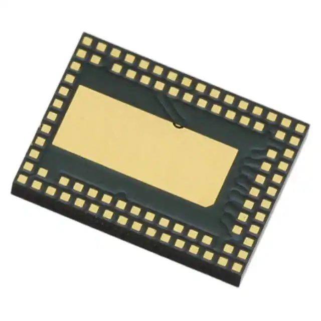


 工商网监
湘ICP备2023018690号
工商网监
湘ICP备2023018690号
