®
BU808DFI
HIGH VOLTAGE FAST-SWITCHING NPN POWER DARLINGTON
s
s
s s s
s s
STMicroelectronics PREFERRED SALESTYPE NPN MONOLITHIC DARLINGTON WITH INTEGRATED FREE-WHEELING DIODE HIGH VOLTAGE CAPABILITY ( > 1400 V ) HIGH DC CURRENT GAIN ( TYP. 150 ) U.L. RECOGNISED ISOWATT218 PACKAGE (U.L. FILE # E81734 (N)) LOW BASE-DRIVE REQUIREMENTS DEDICATED APPLICATION NOTE AN1184
3 2 1
APPLICATIONS s COST EFFECTIVE SOLUTION FOR HORIZONTAL DEFLECTION IN LOW END TV UP TO 21 INCHES. DESCRIPTION The BU808DFI is a NPN transistor in monolithic Darlington configuration. It is manufactured using Multiepitaxial Mesa technology for cost-effective high performance.
ISOWATT218
INTERNAL SCHEMATIC DIAGRAM
ABSOLUTE MAXIMUM RATINGS
Symbol V CBO V CEO V EBO IC I CM IB I BM P t ot T stg Tj June 2000 Parameter Collector-Base Voltage (I E = 0) Collector-Emitter Voltage (IB = 0) Emitter-Base Voltage (IC = 0) Collector Current Collector Peak Current (tp < 5 ms) Base Current Base Peak Current (tp < 5 ms) Total Dissipation at Tc = 25 o C St orage Temperature Max. Operating Junction Temperature Value 1400 700 5 8 10 3 6 52 -65 to 150 150 Uni t V V V A A A A W
o o
C C 1/7
�BU808DFI
THERMAL DATA
R t hj-ca se Thermal Resistance Junction-case Max 2.4
o
C/W
ELECTRICAL CHARACTERISTICS (Tcase = 25 oC unless otherwise specified)
Symb ol I CES I EBO V CE(sat )∗ V BE(s at)∗ h F E∗ Parameter Collector Cut-off Current (V BE = 0) Emitter Cut-off Current (I C = 0) Collector-Emitter Saturation Voltage Base-Emitt er Saturation Voltage DC Current Gain INDUCTIVE LO AD Storage Time Fall Time INDUCTIVE LO AD Storage Time Fall Time Test Cond ition s V CE = 1400 V V EB = 5 V IC = 5 A IC = 5 A IC = 5 A IC = 5 A IB = 0.5 A IB = 0.5 A V CE = 5 V V CE = 5 V 60 20 Min. Typ . Max. 400 100 1.6 2.1 230 Un it µA mA V V
Tj = 100 C
o
ts tf ts tf VF
V CC = 150 V I B1 = 0.5 A V CC = 150 V I B1 = 0.5 A T j = 100 oC
IC = 5 A VBEoff = -5 V IC = 5 A VBEoff = -5 V
3 0.8 2 0.8 3
µs µs µs µs V
Diode F orward Voltage I F = 5 A
∗ Pulsed: Pulse duration = 300 µs, duty cycle 1.5 %
Safe Operating Area
Thermal Impedance
2/7
�BU808DFI
Derating Curve DC Current Gain
Collector Emitter Saturation Voltage
Base Emitter Saturation Voltage
Power Losses at 16 KHz
Switching Time Inductive Load at 16KHz
3/7
�BU808DFI
Switching Time Inductive Load at 16KHZ Reverse Biased SOA
BASE DRIVE INFORMATION In order to saturate the power switch and reduce conduction losses, adequate direct base current IB1 has to be provided for the lowest gain hFE at 100 oC (line scan phase). On the other hand, negative base current IB2 must be provided to turn off the power transistor (retrace phase). Most of the dissipation, in the deflection application, occurs at switch-off. Therefore it is essential to determine the value of IB2 which minimizes power losses, fall time tf and, consequently, Tj. A new set of curves have been defined to give total power losses, ts and tf as a function of IB2 at both 16 KHz scanning frequencies for choosing the optimum negative drive. The test circuit is illustrated in figure 1. Inductance L 1 serves to control the slope of the negative base current IB2 to recombine the excess carrier in the collector when base current is still present, this would avoid any tailing phenomenon in the collector current. The values of L and C are calculated from the following equations: 1 1 1 L (IC)2 = C (VCEfly)2 ω = 2 πf = 2 2 L √C Where IC= operating collector current, VCEfly= flyback voltage, f= frequency of oscillation during retrace.
4/7
�BU808DFI
Figure 1: Inductive Load Switching Test Circuits.
Figure 2: Switching Waveforms in a Deflection Circuit
5/7
�BU808DFI
ISOWATT218 MECHANICAL DATA
DIM. A C D D1 E F F2 F3 G H L L1 L2 L3 L4 L5 L6 N R DIA mm TYP. inch TYP.
MIN. 5.35 3.30 2.90 1.88 0.75 1.05 1.50 1.90 10.80 15.80 20.80 19.10 22.80 40.50 4.85 20.25 2.1
MAX. 5.65 3.80 3.10 2.08 0.95 1.25 1.70 2.10 11.20 16.20 21.20 19.90 23.60 42.50 5.25 20.75 2.3
MIN. 0.211 0.130 0.114 0.074 0.030 0.041 0.059 0.075 0.425 0.622 0.819 0.752 0.898 1.594 0.191 0.797 0.083
MAX. 0.222 0.150 0.122 0.082 0.037 0.049 0.067 0.083 0.441 0.638 0.835 0.783 0.929 1.673 0.207 0.817 0.091
9
0.354
4.6 3.5 3.7 0.138
0.181 0.146
- Weight : 4.9 g (typ.) - Maximum Torque (applied to mounting flange) Recommended 0.8 Nm; Maximum: 1 Nm : - The side of the dissipator must be flat within 80 µm
6/7
P025C/A
�BU808DFI
Information furnished is believed to be accurate and reliable. However, STMicroelectronics assumes no responsibility for the consequences of use of such information nor for any infringement of patents or other rights of third parties which may result from its use. No license is granted by implication or otherwise under any patent or patent rights of STMicroelectronics. Specification mentioned in this publication are subject to change without notice. This publication supersedes and replaces all information previously supplied. STMicroelectronics products are not authorized for use as critical components in life support devices or systems without express written approval of STMicroelectronics. The ST logo is a trademark of STMicroelectronics © 2000 STMicroelectronics – Printed in Italy – All Rights Reserved STMicroelectronics GROUP OF COMPANIES Australia - Brazil - China - Finland - France - Germany - Hong Kong - India - Italy - Japan - Malaysia - Malta - Morocco Singapore - Spain - Sweden - Switzerland - United Kingdom - U.S.A. http://www.st.com
7/7
�
很抱歉,暂时无法提供与“BU808DFI”相匹配的价格&库存,您可以联系我们找货
免费人工找货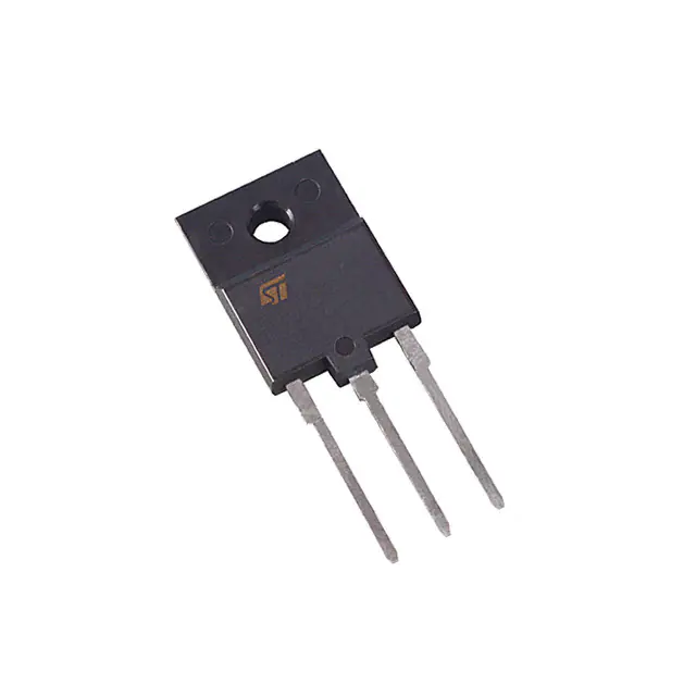


 工商网监
湘ICP备2023018690号
工商网监
湘ICP备2023018690号
