STMPE16M31PX
S-Touch® 16-channel touchkey controller
with proximity sensing
Features
■
Up to 16 capacitive sensor inputs
■
Independent and configurable automatic
calibration on all channels
■
Proximity sensing capability for over 3 cm
distance
■
15 fF resolution, 512 steps with 30 pF autotuning
■
Up to 30 pF external reference capacitor
■
PWM and GPIO:
– Up to 16 general purpose inputs/outputs
– 8 independent PWM controllers, up to 16
PWM outputs
– 12 mA sourcing/sinking on GPIO for LED
driving (at 3.3 V VIO)
– Maximum source/sink current 120 mA
)
s
(
ct
u
d
o
r
P
e
QFN32
(4 x 4 mm)
t
e
l
o
Description
)
(s
■
Operating voltage:
– 1.65 - 1.95 V (VCC, internally supplied)
– 2.7- 5.5 V(VIO)
■
Low operating current: 300 µA in active mode,
40 µA in sleep mode and 5 µA in hibernate
mode
■
I2C
t
c
u
d
o
r
P
e
t
e
l
o
interface (up to 400 kHz). I2C is 3.3 V
tolerant
bs
■
8 kV HBM ESD protection on all sensing pins
OApplications
■
Multimedia bars in notebook computers
■
Portable media players and game consoles
■
Mobile phones and smartphones
Table 1.
s
b
O
The STMPE16M31PX capacitive touchkey
controllers offer highly versatile and flexible
capacitive sensing capabilities in one single chip.
The devices integrate up to 16 capacitive sensing
channels which are highly sensitive and noise
tolerant. Eight independent PWM controllers allow
to control up to 16 LEDs with brightness control,
ramping and blinking capabilities. The I2C
interface supports up to 400 kHz communication
with the system host. A very wide dynamic range
allows most applications to work without
hardware tuning.
A single STMPE16M31PX device can be used to
implement a complete notebook multimedia
control bar with eight capacitive touchkeys,
proximity sensor with sensitivity up to 5 cm and
eight independently controlled LED.
Device summary
Order code
Package
Packaging
STMPE16M31PXQTR
QFN32 (4 x 4 mm)
Tape and reel
January 2011
Doc ID 17058 Rev 2
1/75
www.st.com
75
�Contents
STMPE16M31PX
Contents
1
Pin assignment . . . . . . . . . . . . . . . . . . . . . . . . . . . . . . . . . . . . . . . . . . . . . 4
1.1
Power scheme . . . . . . . . . . . . . . . . . . . . . . . . . . . . . . . . . . . . . . . . . . . . . . 9
1.2
Power states . . . . . . . . . . . . . . . . . . . . . . . . . . . . . . . . . . . . . . . . . . . . . . . . 9
I2C interface module . . . . . . . . . . . . . . . . . . . . . . . . . . . . . . . . . . . . . . . . 10
2
2.1
Device operation . . . . . . . . . . . . . . . . . . . . . . . . . . . . . . . . . . . . . . . . . . . 10
)
s
(
ct
3
Read operations . . . . . . . . . . . . . . . . . . . . . . . . . . . . . . . . . . . . . . . . . . . 14
4
Write operations . . . . . . . . . . . . . . . . . . . . . . . . . . . . . . . . . . . . . . . . . . . 15
4.1
u
d
o
r
P
e
Write operations for one or more bytes . . . . . . . . . . . . . . . . . . . . . . . . . . 15
t
e
l
o
5
General call address . . . . . . . . . . . . . . . . . . . . . . . . . . . . . . . . . . . . . . . . 16
6
Register map and function description . . . . . . . . . . . . . . . . . . . . . . . . . 17
7
System controller . . . . . . . . . . . . . . . . . . . . . . . . . . . . . . . . . . . . . . . . . . 21
7.1
)
(s
s
b
O
Interrupt system . . . . . . . . . . . . . . . . . . . . . . . . . . . . . . . . . . . . . . . . . . . . 25
t
c
u
d
o
r
8
Interrupt service routine . . . . . . . . . . . . . . . . . . . . . . . . . . . . . . . . . . . . . 32
9
GPIO controller . . . . . . . . . . . . . . . . . . . . . . . . . . . . . . . . . . . . . . . . . . . . 33
t
e
l
o
10
s
b
O
11
12
P
e
PWM array controller . . . . . . . . . . . . . . . . . . . . . . . . . . . . . . . . . . . . . . . 37
PWM controller . . . . . . . . . . . . . . . . . . . . . . . . . . . . . . . . . . . . . . . . . . . . 39
11.1
Basic PWM programming . . . . . . . . . . . . . . . . . . . . . . . . . . . . . . . . . . . . 45
12.1
13
2/75
PWM function register map . . . . . . . . . . . . . . . . . . . . . . . . . . . . . . . . . . . 39
Interrupt on basic PWM controller . . . . . . . . . . . . . . . . . . . . . . . . . . . . . . 47
Touch sensor controller . . . . . . . . . . . . . . . . . . . . . . . . . . . . . . . . . . . . . 48
13.1
Sampling rate calculation . . . . . . . . . . . . . . . . . . . . . . . . . . . . . . . . . . . . . 49
13.2
Sensor resolution . . . . . . . . . . . . . . . . . . . . . . . . . . . . . . . . . . . . . . . . . . . 50
Doc ID 17058 Rev 2
�STMPE16M31PX
Contents
13.3
Auto tuning . . . . . . . . . . . . . . . . . . . . . . . . . . . . . . . . . . . . . . . . . . . . . . . . 50
13.4
Locked impedance . . . . . . . . . . . . . . . . . . . . . . . . . . . . . . . . . . . . . . . . . . 52
13.5
Calibration . . . . . . . . . . . . . . . . . . . . . . . . . . . . . . . . . . . . . . . . . . . . . . . . 52
13.6
Definition of data accessible through channel data register . . . . . . . . . . . 59
14
Touchkey and proximity sensing controller . . . . . . . . . . . . . . . . . . . . . 60
15
Maximum rating . . . . . . . . . . . . . . . . . . . . . . . . . . . . . . . . . . . . . . . . . . . . 69
15.1
16
Recommended operating conditions . . . . . . . . . . . . . . . . . . . . . . . . . . . . 69
)
s
(
ct
DC electrical characteristics . . . . . . . . . . . . . . . . . . . . . . . . . . . . . . . . . 70
16.1
u
d
o
Capacitive sensor specification . . . . . . . . . . . . . . . . . . . . . . . . . . . . . . . . 71
r
P
e
17
Package mechanical data . . . . . . . . . . . . . . . . . . . . . . . . . . . . . . . . . . . . 72
18
Revision history . . . . . . . . . . . . . . . . . . . . . . . . . . . . . . . . . . . . . . . . . . . 81
t
e
l
o
)
(s
s
b
O
t
c
u
d
o
r
P
e
t
e
l
o
s
b
O
Doc ID 17058 Rev 2
3/75
�Pin assignment
1
STMPE16M31PX
Pin assignment
Figure 1.
STMPE16M31PX pin out
��
��
��
��
��
��
��
��
�
��
�
��
�
��
�
��
34-0%��-��08
r
P
e
��
�
t
e
l
o
�
�
�
��
��
)
(s
o
s
b
O
4/75
s
b
O
��
��
��
��
��
��
��
t
c
u
d
o
r
Table 2.
!-�����6�
STMPE16M31PX pin description
P
e
let
u
d
o
��
�
)
s
(
ct
Pin number
Pin name
Voltage domain
1
GPIO-0
VIO
GPIO / capacitive sense
2
GPIO-1
VIO
GPIO / capacitive sense
3
GPIO-2
VIO
GPIO / capacitive sense
4
GND
-
Ground
5
VIO
-
I/O supply
6
GPIO-3
VIO
GPIO / capacitive sense
7
GPIO-4
VIO
GPIO / capacitive sense
8
GPIO-5
VIO
GPIO / capacitive sense
9
GPIO-6
VIO
GPIO / capacitive sense
10
GPIO-7
VIO
GPIO / capacitive sense
11
GND
-
Ground
12
VIO
-
I/O supply
13
VCC
-
Doc ID 17058 Rev 2
Description
�STMPE16M31PX
Pin assignment
Table 2.
STMPE16M31PX pin description (continued)
Pin number
Pin name
Description
14
INT
VCC
Open drain interrupt output. This
pin should be pulled to VCC or
GND, depending on polarity of
interrupt used. This pin must not
be left floating.
15
Address 0
VCC
I2C address 0
16
SCL
VCC
I2C clock
17
SDA
VCC
I2C data
18
RESET_N
VCC
Active low reset signal
19
Address 1
VCC
I2C address 1
20
CRef
VCC
Reference capacitor
21
GND
VCC
Ground
22
GPIO-8
VIO
23
GPIO-9
VIO
24
VIO
-
25
GPIO-10
VIO
GPIO / capacitive sense
26
GPIO-11
VIO
GPIO / capacitive sense
27
GPIO-12
VIO
GPIO / capacitive sense
28
GPIO-13
VIO
GPIO / cap sense
)
(s
t
c
u
29
30
31
od
Pr
32
e
t
e
ol
Voltage domain
u
d
o
r
P
e
t
e
l
o
s
b
O
)
s
(
ct
GPIO / capacitive sense
GPIO / capacitive sense
I/O supply
VIO
-
I/O supply
GND
-
I/O voltage supply
GPIO-14
VIO
GPIO / capacitive sense
GPIO-15
VIO
GPIO / capacitive sense
s
b
O
Doc ID 17058 Rev 2
5/75
�Pin assignment
STMPE16M31PX
Figure 2.
Block diagram
6##DOMAIN
6)�/DOMAIN
07-
ARRAY
'0)/
CONTROLLER
!�
!�
2%3%
3$!4
3#,+
).4
t
e
l
o
bs
O
)
6## '.$
du
o
r
P
s
b
O
6/75
Doc ID 17058 Rev 2
u
d
o
r
P
e
#ALIBRATION
s
(
t
c
e
t
e
ol
-58
.OISEFILTER
(OST
INTERFACE
UNIT
)
s
(
ct
#APACITANCESENSOR
'0)/�
��
07-
CONTROLLER
32EF
'.$ 6)/
!-�����6�
�STMPE16M31PX
Pin assignment
Figure 3.
Sample application - notebook multimedia bar
3ENSORPADS
%MBEDDED
CONTROLLER
234
).4 3#,+
3$!4
3ENSOR�
�
)
s
(
ct
07-�
�
2EF
u
d
o
r
P
e
t
e
l
o
Table 3.
)
(s
s
b
O
)NDICATOR,%$S
ct
u
d
o
!-�����6�
Limitations on intrinsic capacitance on PCB / flexi PCB(1)
r
P
e
Cmax-Cmin
(Difference between
highest and lowest channel
capacitance)
Cmax
Matching capacitors
< 30 pF
< 30 pF
Not required
s
b
O
30 pF, < 60 pF
Cref of up to 30 pF required
> 30 pF, < 60 pF
> 30 pF, < 60 pF
Cref of up to 30 pF required
Channel matching capacitance of up
to 25 pF required
> 60 pF
> 60 pF
PCB optimization required
t
e
l
o
1. For small PCBs, it is possible to operate the device with CRef left unconnected. However, without a small
capacitance at this pin, the capacitive sensing operation tends to be noisier. It is recommended that a
capacitor of 10 pF to be connected to this pin.
Doc ID 17058 Rev 2
7/75
�Pin assignment
1.1
STMPE16M31PX
Power scheme
The STMPE16M31PX is powered by a 2.7- 5.5 V supply. An internal voltage regulator
regulates this supply into 1.8 V for core operation. It is recommended to connect a 1 µF
capacitor at VCC pin for filtering purpose. The VIO powers all GPIOs directly, if any LED
driving is required on the GPIO, the VIO should be at least 3.3 V.
Figure 4.
Power supply scheme
STMPE16M31PX
VIO
2.7 - 5.5 V
u
d
o
VCC
1 μF
GND
)
(s
1.2
Power states
)
s
(
ct
r
P
e
t
e
l
o
s
b
O
AM04129V2
t
c
u
d
o
r
The STMPE16M31PX operate in 3 states. Table 4 illustrates the capability of the device in
each of the power states.
P
e
let
Table 4.
so
b
O
8/75
Functions available in each power state
Hibernate
Sleep
Active
2
I C
Yes
Yes
Yes
GPIO hotkey
Yes
Yes
Yes
PWM
No
Yes
Yes
Capacitive sensing
No
Slow
Yes
Proximity sensor
No
No
Yes
Doc ID 17058 Rev 2
�I2C interface module
STMPE16M31PX
I2C interface module
2
The STMPE16M31PX has 2 physical I2C address pins, allowing 4 different I2C address
settings.
I2C address pins
Table 5.
Address 1
Address 0
I2C address
0
0
0x58
0
1
0x59
1
0
0x5A
1
1
0x5B
)
s
(
ct
u
d
o
The features that are supported by the I2C interface module are the following ones:
–
I2C slave device
–
Operates at VCC
r
P
e
2
t
e
l
o
–
Compliant to Philips I C specification version 2.1
–
Supports standard (up to 100 kbps) and fast (up to 400 kbps) modes
–
7-bit and 10-bit device addressing modes
–
General call
–
Start/restart/stop
)
(s
s
b
O
The features that are not supported are:
2.1
–
Hardware general call
–
CBUS compatibility
–
High-speed (3.4 Mbps) mode
t
c
u
d
o
r
P
e
Device operation
t
e
l
o
Start condition
O
bs
A Start condition is identified by a falling edge of SDA while SCL is stable at high state. A
Start condition must precede any data/command transfer. The device continuously
monitors for a Start condition and does not respond to any transaction unless one is
encountered.
Stop condition
A Stop condition is identified by a rising edge of SDA while SCL is stable at high state. A
Stop condition terminates the communication between the slave device and bus master. A
read command that is followed by NoAck can be followed by a Stop condition to force the
slave device into idle mode. When the slave device is in idle mode, it is ready to receive the
next I2C transaction. A Stop condition at the end of a write command stops the write
operation to registers.
Doc ID 17058 Rev 2
9/75
�I2C interface module
STMPE16M31PX
Acknowledge bit (ACK)
The acknowledge bit is used to indicate a successful byte transfer. The bus transmitter
releases the SDA after sending eight bits of data. During the ninth bit, the receiver pulls the
SDA low to acknowledge the receipt of the eight bits of data. The receiver may leave the
SDA in high state if it would to not acknowledge the receipt of the data.
Data input
The device samples the data input on SDA on the rising edge of the SCL. The SDA signal
must be stable during the rising edge of SCL and the SDA signal must change only when
SCL is driven low.
Memory addressing
)
s
(
ct
For the bus master to communicate to the slave device, the bus master must initiate a Start
condition and be followed by the slave device address. Accompanying the slave device
address, there is a Read/W bit (R/W). The bit is set to 1 for Read and 0 for Write operation.
u
d
o
If a match occurs on the slave device address, the corresponding device gives an
acknowledgement on the SDA during the 9th bit time. If there is no match, it deselects itself
from the bus by not responding to the transaction. The register memory map of the device is
8-bit address width. Therefore, the maximum number of register is 256 registers of 8-bit
width.
r
P
e
t
e
l
o
s
b
O
Table 6 illustrates the device operating modes that are supported.
Table 6.
Device operation modes
Mode
)-
Bytes
Initial sequence
s
(
t
c
START, Device Address, R/W
=0, Base register Address to be read
e
t
e
ol
s
b
O
10/75
du
o
r
P
Read
≥1
ReSTART, Device Address, R/W
=1, Data Read, STOP
If no STOP is issued, the Data Read can be continuously
preformed. The address is automatically incremented on
subsequent data read.
START, Device Address, R/W
=0, Register Address to be written, Data Write, STOP
Write
≥1
If no STOP is issued, the Data Write can be continuously
performed. The address is automatically incremented on
subsequent write.
Doc ID 17058 Rev 2
�I2C interface module
STMPE16M31PX
r
P
e
Da ta to
W r ite + 2
Stop
Stop
Ack
NoAck
Da ta
Re a d + 2
…
Stop
Ack
Ack
Da ta
Re a d
Ack
RnW=1
RnW=1
Da ta
Re a d
Ack
Stop
Da ta to
W r ite + 1
Ack
reStart
Da ta to
W r ite
Ack
reStart
Ack
Da ta to
W r ite
Da ta
Re a d + 1
Ack
Re g
A ddr
Da ta
Re a d
( 2 M SB )
Ack
( 8 LSB )
Ack
Ack
Ack
RnW=0
Ack
De v
A ddr
Re g
A ddr
…
( 2 M SB )
De v
A ddr
11110
Ack
(2 M SB )
( 8 LSB )
r
P
e
De v
A ddr
11110
t
e
l
o
s
b
O
De v
A ddr
u
d
o
Ack
De v
A ddr
Re g
A ddr
Ack
(2 M SB )
Re g
A ddr
Ack
u
d
o
11110
RnW=0
s
(
t
c
11110
De v
A ddr
)Ack
De v
A ddr
( 8 LSB )
RnW=0
De v
A ddr
Ack
Start
Start
(2 M SB )
De v
A ddr
( 8 LSB )
RnW=0
M o r e th an
O n e By t e
W r it e
t
e
l
o
11110
Start
O n e By t e
W r it e
(2 M SB )
Start
M o r e th an
O n e By t e
Re a d
De v
A ddr
11110
Ack
I2 C Tra n s a c t io n U s in g 7 -B it A d d re s s in g
NoAck
)
s
(
ct
M a s te r
S la ve
O n e By t e
Re a d
Stop
NoAck
Ack
Stop
Da ta to
W r ite + 2
Da ta
Re a d + 2
Stop
NoAck
Ack
Da ta
Re a d + 1
Ack
Da ta to
W r ite + 1
Ack
Ack
RnW=1
Ack
RnW=1
Stop
Da ta to
W r ite
Da ta
Re a d
Ack
reStart
reStart
Da ta to
be
W r itte n
Da ta
Re a d
Ack
Ack
Ack
Re g
A ddr
De v
A ddr
Ack
Re g
A ddr
De v
A ddr
Ack
Ack
RnW=0
Ack
RnW=0
RnW=0
De v
A ddr
Re g
A ddr
Ack
De v
A ddr
Re g
A ddr
Ack
M o r e th an
O n e By t e
W r it e
De v
A ddr
RnW=0
O n e By t e
W r it e
Start
M o r e th an
O n e By t e
Re a d
De v
A ddr
Start
O n e By t e
Re a d
Start
Read and write modes (random and sequential)
Start
Figure 5.
M a s te r
S la ve
I2 C Tra n s a c t io n U s in g 1 0 -B it A d d re s s in g
s
b
O
Doc ID 17058 Rev 2
11/75
�I2C interface module
Figure 6.
STMPE16M31PX
Flow diagram for read and write modes
-ASTER
34!24
3LAVE
34!24
$EVICE!DDR�
2N7��
.O!CK
)
s
(
ct
!CK
!DDROF2EG
r
P
e
t
e
l
o
!CK
s
b
O
RE34!24
)-
s
(
t
c
u
d
o
e
t
e
ol
s
b
O
Pr
$EVICE!DDR�
2N7��
u
d
o
$ATA7RITE�I
!CK
!CK
$ATA2EAD�
I
!CK
.O!CK
34/0
%.$
!-�����6�
12/75
Doc ID 17058 Rev 2
�STMPE16M31PX
3
Read operations
Read operations
Read operations for one or more bytes
A write is first performed to load the base register address into the address counter but
without sending a Stop condition. Then, the bus master sends a reStart condition and
repeats the Device Address with the R/W bit set to 1. The slave device acknowledges and
outputs the content of the addressed byte. If no more data is to be read, the bus master
must not acknowledge the byte and terminates the transfer with a Stop condition.
If the bus master acknowledges the data byte, then it can continue to perform the data
reading. To terminate the stream of data byte, the bus master must not acknowledge the
last output byte and follow by a Stop condition. The data fetched are from consecutive
addresses. After the last memory address, the Address Counter 'rolls-over' and the device
continue to output data from the memory address of 0x00.
)
s
(
ct
u
d
o
Acknowledgement in read operation
r
P
e
For the above read command, the slave device waits, after each byte read, for an
acknowledgement during the 9th bit time. If the bus master does not drive the SDA to low
state (no acknowledgement by the master), then the slave device terminates and switches
back to its idle mode, waiting for the next command.
t
e
l
o
)
(s
s
b
O
t
c
u
d
o
r
P
e
t
e
l
o
s
b
O
Doc ID 17058 Rev 2
13/75
�Write operations
STMPE16M31PX
4
Write operations
4.1
Write operations for one or more bytes
A write is first performed to load the base register address into the Address Counter without
sending a Stop condition. After the bus master receives an acknowledgement from the
slave device, it may start to send a data byte to the register (pointed by the Address
Counter). The slave device again acknowledges and the bus master terminates the transfer
with a Stop condition.
If the bus master would like to continue to write more data, it can just continue write
operation without issuing the Stop condition. After the bus master writes the last data byte
and the slave device acknowledges the receipt of the last data, the bus master may
terminate the write operation by sending a Stop condition. When the Address Counter
reaches the last memory address, it 'rolls-over' on the next data byte write.
)
s
(
ct
u
d
o
r
P
e
t
e
l
o
)
(s
s
b
O
t
c
u
d
o
r
P
e
t
e
l
o
s
b
O
14/75
Doc ID 17058 Rev 2
�STMPE16M31PX
5
General call address
General call address
A general call address is a transaction with the slave address of 0x00 and R/W = 0. When a
general call address is made, the GPIO expander responds to this transaction with an
acknowledgement and behaves as a slave-receiver mode. The meaning of a general call
address is defined in the second byte sent by the master-transmitter.
Definition of the second byte of the I2C transaction
Table 7.
R/W
Second byte
value
0
0x06
2-byte transaction in which the second byte tells the slave device to
perform a soft reset and write (or latch in) the 2-bit programmable part of
the slave address.
0
0x04
2-byte transaction in which the second byte tells the slave device not to
perform a soft reset and write (or latch in) the 2-bit programmable part of
the slave address.
0
0x00
Not allowed as second byte.
Definition
)
s
(
ct
u
d
o
r
P
e
t
e
l
o
Note:
All other second byte values will be ignored.
Note:
Please allow a gap of approximately 2 µs gap before the next I2C transaction after the
General Call of 0x04 or 0x06.
)
(s
s
b
O
t
c
u
d
o
r
P
e
t
e
l
o
s
b
O
Doc ID 17058 Rev 2
15/75
�Register map and function description
6
STMPE16M31PX
Register map and function description
This section lists and describes the registers of the STMPE16M31PX device, starting with a
register map and then provides detailed descriptions of register types.
Table 8.
Register map
Address
Register name
Reset value
I2C
0x00
CHIP_ID
0x2431
R
CHIP identification number
MSB: 0x24, LSB: 0x32
Version of device
Engineering samples:
0x01, 0x02
Final silicon: 0x03
ID_VER
0x03
R
0x03
SYSCON-1
0x00
RW
0x04
SYSCON-2
0xFE
RW
Sensor and PWM clock divider
0x06
INT_CTRL
0x00
RW
Interrupt control
0x08
INT_STA
0x00
0x09
INT_EN
0x0A
GPIO_INT_STA
0x0C
GPIO_INT_EN
0x0E
PWM_INT_STA
0x0F
0x10
r
P
e
let
Interrupt status
RW
Interrupt enable
0x0000
RW
Interrupt status GPIO
0x0000
RW
Interrupt enable GPIO
0x00
RW
Interrupt status PWM
PWM_INT_EN
0x00
RW
Interrupt enable PWM
GPIO_DIR
0x0000
RW
GPIO direction setting
GPIO_MP_STA
0x0000
R
GPIO pin state monitor
GPIO_SET_PIN
0x0000
RW
GPIO set pin state
0x16
GPIO_ALT_FUN
0x0000
RW
GPIO alternate function
0x20
GPIO_0_PWM_CFG
0x00
RW
Configures PWM output of
GPIO-0
0x21
GPIO_1_PWM_CFG
0x00
RW
Configures PWM output of
GPIO-1
0x22
GPIO_2_PWM_CFG
0x00
RW
Configures PWM output of
GPIO-2
0x23
GPIO_3_PWM_CFG
0x00
RW
Configures PWM output of
GPIO-3
0x24
GPIO_4_PWM_CFG
0x00
RW
Configures PWM output of
GPIO-4
0x25
GPIO_5_PWM_CFG
0x00
RW
Configures PWM output of
GPIO-5
0x26
GPIO_6_PWM_CFG
0x00
RW
Configures PWM output of
GPIO-6
e
t
e
ol
16/75
u
d
o
General system control
RW
)
s
(
ct
u
d
o
Pr
0x14
O
)
s
(
ct
0x02
0x12
bs
Register function
o
s
b
0x00
-O
Doc ID 17058 Rev 2
�STMPE16M31PX
Register map and function description
Table 8.
Register map (continued)
Address
Register name
Reset value
I2C
0x27
GPIO_7_PWM_CFG
0x00
RW
Configures PWM output of
GPIO-7
0x28
GPIO_8_PWM_CFG
0x00
RW
Configures PWM output of
GPIO-8
0x29
GPIO_9_PWM_CFG
0x00
RW
Configures PWM output of
GPIO-9
0x2A
GPIO_10_PWM_CFG
0x00
RW
Configures PWM output of
GPIO-10
0x2B
GPIO_11_PWM_CFG
0x00
RW
Configures PWM output of
GPIO-11
Configures PWM output of
GPIO-12
GPIO_12_PWM_CFG
0x00
RW
0x2D
GPIO_13_PWM_CFG
0x00
RW
Configures PWM output of
GPIO-13
r
P
e
0x2E
GPIO_14_PWM_CFG
0x00
RW
0x2F
GPIO_15_PWM_CFG
0x00
RW
Configures PWM output of
GPIO-15
0x30
PWM_MASTER_EN
0x00
RW
PWM master enable
0x40
PWM_0_SET
0x00
RW
PWM0 setup
0x41
PWM_0_CTRL
0x00
RW
PWM0 control
0x42
PWM_0_RAMP_RATE
0x00
RW
PWM0 ramp rate
PWM_0_TRIG
0x00
RW
PWM0 trigger
PWM_1_SET
0x00
RW
PWM1 setup
PWM_1_CTRL
0x00
RW
PWM1 control
0x46
PWM_1_RAMP_RATE
0x00
RW
PWM1 ramp rate
0x47
PWM_1_TRIG
0x00
RW
PWM1 trigger
0x48
PWM_2_SET
0x00
RW
PWM2 setup
0x49
PWM_2_CTRL
0x00
RW
PWM2 control
0x4A
PWM_2_RAMP_RATE
0x00
RW
PWM2 ramp rate
0x4B
PWM_2_TRIG
0x00
RW
PWM2 trigger
0x4C
PWM_3_SET
0x00
RW
PWM3 setup
0x4D
PWM_3_CTRL
0x00
RW
PWM3 control
0x4E
PWM_3_RAMP_RATE
0x00
RW
PWM3 ramp rate
0x4F
PWM_3_TRIG
0x00
RW
PWM3 trigger
0x50
PWM_4_SET
0x00
RW
PWM4 setup
0x51
PWM_4_CTRL
0x00
RW
PWM4 control
0x52
PWM_4_RAMP_RATE
0x00
RW
PWM4 ramp rate
)-
s
(
t
c
du
ro
P
e
0x45
O
u
d
o
Configures PWM output of
GPIO-14
0x44
bs
)
s
(
ct
0x2C
0x43
t
e
l
o
Register function
t
e
l
o
s
b
O
Doc ID 17058 Rev 2
17/75
�Register map and function description
Table 8.
Register map (continued)
Address
Register name
Reset value
I2C
0x53
PWM_4_TRIG
0x00
R/W
PWM4 trigger
0x54
PWM_5_SET
0x00
R/W
PWM5 setup
0x55
PWM_5_CTRL
0x00
R/W
PWM5 control
0x56
PWM_5_RAMP_RATE
0x00
R/W
PWM5 ramp rate
0x57
PWM_5_TRIG
0x00
R/W
PWM5 trigger
0x58
PWM_6_SET
0x00
R/W
PWM6 setup
0x59
PWM_6_CTRL
0x00
R/W
PWM6 control
0x5A
PWM_6_RAMP_RATE
0x00
R/W
PWM6 ramp rate
0x5B
PWM_6_TRIG
0x00
R/W
PWM6 trigger
0x5C
PWM_7_SET
0x00
R/W
PWM7 setup
0x5D
PWM_7_CTRL
0x00
R/W
PWM7 control
0x5E
PWM_7_RAMP_RATE
0x00
R/W
PWM7 ramp rate
0x5F
PWM_7_TRIG
0x00
R/W
PWM7 trigger
0x70
CAP_SEN_CTRL
0x00
R/W
Capacitive sensor control
0x71
RATIO_ENG_REPT_C
TRL
0x00
R/W
Ratio engine report control
(only available in final silicon)
0x72
CH_SEL
0x00000000
R/W
Selects active capacitive
channels
CAL_INT
0x00
R/W
10 ms – 64 s calibration interval
CAL_MOD
0x00
R/W
Selects calibration model
MAF_SET
0x00
R/W
Control of median averaging
filter
)
s
(
ct
0x76
0x77
0x78
u
d
o
r
P
e
t
e
l
o
bs
STMPE16M31PX
-O
u
d
o
0x7C
DATA_TYPE
0x00
R/W
Selects type of data available in
channel data ports.
0x01: TVR
0x02: EVR
0x03: Channel delay
0x04: Impedance (13-bit)
0x05:Calibrated Impedance (13bit)
0x06:Locked impedance (13-bit)
0x90
KEY_PROX_CTRL
0x00
R/W
General key filter control
0x92
KEY_FILT_GROUP-1
0x00000000
R/W
Define channels included in key
filter group 1
0x96
PROX_CFG
0x00
R/W
proximity configuration register
0x97
PTVR
0x00
R/W
TVR used for proximity sensing
0x98
PEVR
0x00
R/W
EVR used for proximity sensing
and forced proximity calibration
O
18/75
)
s
(
ct
r
P
e
t
e
l
o
bs
Register function
Doc ID 17058 Rev 2
�STMPE16M31PX
Register map and function description
Table 8.
Register map (continued)
Address
Register name
Reset value
I2C
0xB1
PEPort1
0x00
R
Proximity data 1
0xBO
PEPort0
0x00
R
Proximity data O
0x9A
KEY_FILT_DATA
0x00000000
0xB4
TOUCH_DET
0x00000000
0xC0
CH_DATA-0
0x0000
0xC2
CH_DATA-1
0x0000
0xC4
CH_DATA-2
0x0000
0xC6
CH_DATA-3
0x0000
0xC8
CH_DATA-4
0x0000
0xCA
CH_DATA-5
0x0000
0xCC
CH_DATA-6
0x0000
0xCE
CH_DATA-7
0x0000
0xD0
CHDATA-8
0x0000
0xD2
CH_DATA-9
0xD4
CH_DATA-10
0xD6
CH_DATA-11
0xD8
CH_DATA-12
0xDA
CH_DATA-13
o
r
P
0xDE
0xE0
e
t
e
ol
ct
du
0xDC
(s)
-O
Filtered touchkey data
R
Touch detection register
(real time)
)
s
(
ct
u
d
o
r
P
e
let
o
s
b
0x0000
Register function
R
Channel data according to data
type setting
0x0000
0x0000
0x0000
0x0000
CH_DATA-14
0x0000
CH_DATA-15
0x0000
CH_DATA-16
0x0000
s
b
O
Doc ID 17058 Rev 2
19/75
�System controller
7
STMPE16M31PX
System controller
The system controller contains the registers that control the following functions:
–
Device identification
–
Version identification
–
Power state management
–
Clock speed management
–
Clock gating to various modules
Table 9.
System controller registers
Register name
Reset value
R/W
0x00
CHIP_ID
0x2432
R
CHIP identification number
MSB: 0x24, LSB: 0x32
0x02
ID_VER
0x03
R
Version of device
0x03
SYSCON-1
0x00
RW
General system
control
0x04
SYSCON-2
0xFE
)
(s
d
o
r
P
e
t
e
l
o
s
b
O
Doc ID 17058 Rev 2
Description
u
d
o
r
P
e
t
e
l
o
s
b
O
t
c
u
20/75
)
s
(
ct
Address
RW
Sensor and PWM clock divider
�STMPE16M31PX
System controller
SYSCON-1
General system control
Address:
0x03
Type:
R/W
Reset:
0x00
Description:
The general system control register (SYSCON-1) controls the operation state and
clock speed of the device.
7
6
5
4
3
2
1
0
RESERVED
RESERVED
RESERVED
CLKSPD
SLEEP_EN
Reserved
SOFT_RST
HIBRNT
RW
RW
RW
RW
RW
RW
RW
RW
1
1
1
1
1
1
1
)
s
(
ct
0
[7:5] RESERVED: Do not write to these bits. Reads ‘0’. Writing ‘1’ to these bits may result in
unpredictable behaviour.
u
d
o
[4] CLKSPD: Selects the macro engine’s speed.
0: 2 MHz
1: RESERVED
r
P
e
t
e
l
o
[3] SLEEP_EN: Enable or disable the sleep mode. Under all operating conditions, this bit should
be set to '0'.
1: Enable the touch sensor’s sleep mode
0: Disable the touch sensor’s sleep mode
)
(s
s
b
O
[2] RESERVED: Do not write to these bits. Reads ‘0’.
[1] SOFT_RST: Soft reset.
1: To perform soft reset.
t
c
u
[0] HIBRNT: Hibernate.
1: To force the device to hibernate mode.
d
o
r
P
e
t
e
l
o
s
b
O
Doc ID 17058 Rev 2
21/75
�System controller
STMPE16M31PX
SYSCON-2
Sensor and PWM clock divider
Address:
0x04
Type:
R/W
Reset:
0xFE
Description:
Sensor and PWM clock divider. The SYSCON-2 register controls the sensor and
PWM clock speed, and the clock gating of various functional modules.
This bit will always read '0'. as the I2C transaction to read this bit will wake up the
device from hibernate mode.
7
6
5
4
3
2
1
0
GPIO_CLK
PWM_CLK
CS_CLK
SCLK_DIV
PCLK_DIV
RW
RW
RW
1
1
1
)
s
(
ct
RW
0
u
d
o
r
P
e
[7:5] SCLK_DIV: Sensor clock divider.
000, 001: RESERVED
010 : 32 (to be used only if load capacitance is < 30 pF)
011: 64
100: 128
101: 256
110: 512
111: 1024
Sensor clock is 2 MHz / ( PRBS_Factor * SCLK_DIV[2:0] )
PRBS factor is a pseudo-random sequence of number, ranging from 1-8. This is used to reduce
the effect of surrounding EMI on the sensor. Average of this factor is approximately 2.5
Effective sampling rate is 2 MHz/ (2.5*SCLK_DIV[2:0]).
Maximum total sampling rate : 2MHz/(2.5*64) = 12.5 kHz
Minimum total sampling rate : 2 MHz/(2.5*1024) = 780 Hz
If N channel is active, the per-channel sampling rate is “total sampling rate / N”.
Maximum channel sampling rate = 12.5 kHz/24 = 521 Hz
t
e
l
o
)
(s
s
b
O
t
c
u
d
o
r
P
e
t
e
l
o
s
b
O
22/75
[4:3] PCLK_DIV: PWM clock divider
00 for 16 kHz
01 for 32 kHz
10 for 64 kHz
11 for 128 kHz
Doc ID 17058 Rev 2
�STMPE16M31PX
System controller
[2] PMW_CLK: PWM clock disable
Write “1“ to disable the clock to PWM module.
When clock to PWM module is disabled, access to PWM module register will not work correctly.
[1] GPIO_CLK: GPIO clock disable
Write “1” to diWrite “1“ to disable the clock to GPIO module.
When clock to GPIO module is disabled, access to GPIO module register will not work correctly.
[0] CS_CLK: Capacitive sensor clock disable
Write “1“ to disable the clock to capactive sensor module
When clock to touch module is disabled, access to touch module registers will not work
correclty.
)
s
(
ct
u
d
o
r
P
e
t
e
l
o
)
(s
s
b
O
t
c
u
d
o
r
P
e
t
e
l
o
s
b
O
Doc ID 17058 Rev 2
23/75
�System controller
7.1
STMPE16M31PX
Interrupt system
This module controls the interruption to the host based on the activity of other modules in
the system, such as the capacitive sensing, GPIO and PWM modules.
Figure 7.
Interrupt system
'0)/
EVENTS
07-
EVENTS
'0)/
STATUS
���
BIT
)
s
(
ct
du
07-
STATUS
��
BIT
e
t
e
ol
o
r
P
3YSTEMEVENTS�
bs
).4
STATUS
4OU CHSCREEN
%NVIRONMENTALARM
O
)
s
(
t
c
u
d
o
Pr
Table 10.
e
t
e
ol
s
b
O
24/75
!-�����6�
Interrupt system registers
Address
Register name
Reset value
R/W
0x06
INT_CTRL
0x00
RW
Interrupt control register
0x08
INT_STA
0x00
RW
Interrupt status register
0x09
INT_EN
0x00
RW
Interrupt enable register
0x0A
GPIO_INT_STA
0x0000
RW
Interrupt status GPIO register
0x0C
GPIO_INT_EN
0x0000
RW
Interrupt enable GPIO register
0x0E
PWM_INT_STA
0x00
RW
Interrupt status PWM register
0x0F
PWM_INT_EN
0x00
RW
Interrupt enable PWM register
Doc ID 17058 Rev 2
Description
�STMPE16M31PX
System controller
INT_CTRL
Interrupt control register
Address:
0x06
Type:
R/W
Reset:
0x00
Description:
SYSCON3 controls the interrupt signal generation.
7
6
RW
RW
0
0
5
4
3
RW
RW
RW
0
0
0
RESERVED
2
1
0
INT_POL
INT_TYPE
INT_EN
RW
RW
RW
0
0
0
[7:3] RESERVED
u
d
o
[2] INT_POL: Interrupt polarity
0: Active low
1: Active high
[1] INT_TYPE: Interrupt trigger type
0: Level trigger
1: Edge trigger
[0] INT_EN: Interrupt enable
1: Enable the interrupt
0: Disable the interrupt
)
(s
)
s
(
ct
r
P
e
t
e
l
o
s
b
O
t
c
u
d
o
r
P
e
t
e
l
o
s
b
O
Doc ID 17058 Rev 2
25/75
�System controller
STMPE16M31PX
INT_STA
Interrupt status register
Address:
0x08
Type:
R/W
Reset:
0x00
Description:
This register holds interrupt status from each event.
7
6
5
4
3
2
1
0
GPIO
PWM
WAKEUP
ENV
EOC
TOUCH
PROX
RESERVED
RW
RW
RW
RW
RW
RW
RW
-
0
0
0
0
0
0
0
0
[7] GPIO: Activity in GPIO
Read ‘1’ if GPIO event occurs
Write ‘1’ to clear the interrupt status
)
s
(
ct
u
d
o
r
P
e
[6] PWM: Any channel of PWM has completed the programmed sequence
Read ‘1’ if PWM event occurs
Write ‘1’ to clear the interrupt status
t
e
l
o
[5] Device wake up from SLEEP or HIBERNATE mode
Read ‘1’ if wake-up event occurs
Write ‘1’ to clear the interrupt status
)
(s
s
b
O
[4] ENV: Possible drastic/abnormal environmental changes that requires attention from system
software. This event includes ‘calibration stuck’ and ‘tuning out of range’. If this bit is set, it is
recommended that the host software initiates an unconditional calibration.
Read ‘1’ if the events occur
Write ‘1’ to clear the interrupt status
t
c
u
d
o
r
[3] EOC: End of calibration
Read ‘1’ if the host-triggered calibration has completed
Write ‘1’ to clear the interrupt status
P
e
t
e
l
o
s
b
O
[2] TOUCH: Touch-key event
Read ‘1’ if touch is detected
Write ‘1’ to clear the interrupt status
[1] PROX: Proximity sensor event
Read ‘1’ if proximity sensor detects an object
Write ‘1’ to clear the interrupt status
[0] RESERVED
26/75
Doc ID 17058 Rev 2
�STMPE16M31PX
System controller
INT_EN
Interrupt enable register
Address:
0x09
Type:
R/W
Reset:
0x00
Description:
Controls interrupt source enable.
7
6
5
4
3
2
1
0
GPIO
PWM
WAKEUP
ENV
EOC
TOUCH
PROX
RESERVED
RW
RW
RW
RW
RW
RW
RW
W
0
0
0
0
0
0
0
0
[7] GPIO: Activity in GPIO
Write ‘1’ to enable interrupt signal from GPIO
Write ‘0’ to disable interrupt signal from GPIO
)
s
(
ct
u
d
o
r
P
e
[6] PWM: Any channel of PWM has completed the programmed sequence
Write ‘1’ to enable interrupt signal from PWM
Write ‘0’ to disable interrupt signal from PWM
t
e
l
o
[5] Device wake up from SLEEP or HIBERNATE mode
Read ‘1’ if wake-up event occurs
Write ‘1’ to clear the interrupt status
)
(s
s
b
O
[4] ENV: Possible drastic/abnormal environmental changes that requires attention from system
software. This event includes ‘calibration stuck’ and ‘tuning out of range’
Write ‘1’ to enable interrupt signal from calibration/tuning event
Write ‘0’ to disable interrupt signal from calibration/tuning event
t
c
u
d
o
r
[3] EOC: End of calibration
Write ‘1’ to enable interrupt signal from end of calibration event
Write ‘0’ to disable interrupt signal from end of calibration event
P
e
s
b
O
t
e
l
o
[2] TOUCH: Touchkey event
System should access touch detection register when this interrupt is received.
Touch interrupt source needs to be enabled to activate key filter data.
Write ‘1’ to enable interrupt signal from touch event
Write ‘0’ to disable interrupt signal from touch event
[1] PROX: Proximity sensor event
Write ‘1’ to enable interrupt signal from proximity sensor
[0] RESERVED
Write ‘0’ to disable interrupt signal from proximity sensor
Doc ID 17058 Rev 2
27/75
�System controller
STMPE16M31PX
GPIO_INT_STA
Interrupt status GPIO register
Address:
0x0A – 0x0B
Type:
R/W
Reset:
0x0000
Description:
This register reflects the status of GPIO that has been configured as input. When
there is a change in GPIO state, the corresponding bit will be set to ‘1’ by hardware.
Writing ‘1’ to the corresponding bit clears it. Writing ‘0’ has no effect.
LSB (0x0A)
7
6
5
4
3
2
1
IO-7
IO-6
IO-5
IO-4
IO-3
IO-2
IO-1
RW
RW
RW
RW
RW
RW
RW
0
0
0
0
0
0
0
MSB (0x0B)
7
6
5
4
3
IO-15
IO-14
IO-13
IO-12
IO-11
RW
RW
RW
RW
RW
0
0
0
0
)
(s
so
e
t
e
l
b
O
0
2
o
r
P
d
o
r
P
e
t
e
l
o
s
b
O
28/75
Doc ID 17058 Rev 2
IO-0
RW
0
1
0
IO-10
IO-9
IO-8
RW
RW
RW
0
0
0
[7:0] IO - X: Interrupt status of GPIO - X
Read ‘1’ if state transition is detected in corresponding GPIO channel
Write’1’ to clear the interrupt staus.
t
c
u
du
)
s
(
ct
0
�STMPE16M31PX
System controller
GPIO_INT_EN
Interrupt enable GPIO register
Address:
0x0C – 0x0D
Type:
R/W
Reset:
0x0000
Description:
This register is used to enable the generation of interrupt signal, at the INT pin.
LSB (0x0C)
7
6
5
4
3
2
1
0
IO-7
IO-6
IO-5
IO-4
IO-3
IO-2
IO-1
IO-0
RW
RW
RW
RW
RW
RW
RW
0
0
0
0
0
0
0
7
6
5
4
3
2
IO-15
IO-14
IO-13
IO-12
IO-11
IO-10
RW
RW
RW
RW
RW
0
0
0
0
0
MSB (0x0D)
u
d
o
l
o
s
ete
RW
)
s
(
ct
Pr
0
RW
0
1
0
IO-9
IO-8
RW
RW
0
0
b
O
[7:0] IO - X
Interrupt status of GPIO - X
Read ‘1’ if state transition is detected in corresponding GPIO channel
Write’1’ to clear the interrupt staus.
)
(s
r
P
e
Address:
Type:
0x0E
t
e
l
o
Reset:
Description:
s
b
O
t
c
u
od
PWM_INT_STA
Interrupt status PWM register
R/W
0x00
When a PWM controller completes the PWM sequence, the corresponding bit in this
register goes to ‘1’. Write ‘1’ in this register clears the written bit, writing ‘0’ has no
effect.
7
6
5
4
3
2
1
0
PWM-7
PWM-6
PWM-5
PWM-4
PWM-3
PWM-2
PWM-1
PWM-0
RW
RW
RW
RW
RW
RW
RW
RW
0
0
0
0
0
0
0
0
[7:0] PWM - X
Interrupt status of PWM – X.
Read ‘1’ if the corresponding PWM channel complete programmed sequence
Write ‘1’ to clear the interrupt status
Doc ID 17058 Rev 2
29/75
�System controller
STMPE16M31PX
PWM_INT_EN
Interrupt enable PWM enable register
Address:
0x0F
Type:
R/W
Reset:
0x00
Description:
Writing ‘1’ to this register enables the generation of INT by the corresponding PWM
channel.
7
6
5
4
3
2
1
0
PWM-7
PWM-6
PWM-5
PWM-4
PWM-3
PWM-2
PWM-1
PWM-0
RW
RW
RW
RW
RW
RW
RW
RW
0
0
0
0
0
0
0
)
s
(
ct
[7:0] PWM - X
Enable of PWM – X.
Write ‘1’ to the corresponding bit to enable interrupt generated by a PWM channel
u
d
o
r
P
e
t
e
l
o
)
(s
s
b
O
t
c
u
d
o
r
P
e
t
e
l
o
s
b
O
30/75
Doc ID 17058 Rev 2
0
�STMPE16M31PX
8
Interrupt service routine
Interrupt service routine
On receiving an interrupt, system software should:
Read InterruptStatus
If (GPIO.bit==1)
{
Read InterruptStatusGPIO
Process GPIO INT
)
s
(
ct
Write InterruptStatusGPIO to clear the corresponding bit
Write InterruptStatus to clear the corresponding bit
u
d
o
}
r
P
e
If (PWM.bit==1)
t
e
l
o
{
Read InterruptStatusPWM
Process PWM INT
)
(s
s
b
O
Write InterruptStatusPWM to clear the corresponding bit
Write InterruptStatus to clear the corresponding bit
t
c
u
}
d
o
r
If ( EV_ALARM or TOUCHSCREEN or TOUCHKEY)
P
e
{
t
e
l
o
Process INT
s
b
O
Write InterruptStatus to clear the corresponding bit
}
Doc ID 17058 Rev 2
31/75
�GPIO controller
9
STMPE16M31PX
GPIO controller
A total of 16 GPIOs are available in the STMPE16M31PX. Most of the GPIOs are sharing
physical pins with some alternate functions. The GPIO controller contains the registers that
allow the host system to configure each of the pins into either a GPIO, or one of the
alternate functions. Unused GPIOs should be configured as outputs to minimize the power
consumption.
Table 11.
GPIO controller registers
Address
Register name
Reset value
R/W
0x10
GPDR
0X0000
R/W
GPIO direction register
0x12
GPMR
0X0000
R/W
GPOIO monitor pin state register
0x14
GPSR
0X0000
R/W
GPIO set pin register
0x16
GPFR
0X0000
R/W
GPIO alternate function register
0x10 – 0x11
Type:
RW
Reset:
0x00
Description:
Direction seeting of the GPIO.
LSB (0x10)
IO-7
IO-6
RW
RW
0
0
e
t
e
ol
MSB (0x11)
7
)
(s
t
c
u
5
GPIO direction register
s
b
O
4
3
2
1
0
IO-5
IO-4
IO-3
IO-2
IO-1
IO-0
RW
RW
RW
RW
RW
RW
0
0
0
0
0
0
od
Pr
u
d
o
t
e
l
o
Address:
6
)
s
(
ct
r
P
e
GPIO_DIR
7
Description
6
5
4
3
2
1
0
IO-15
IO-14
IO-13
IO-12
IO-11
IO-10
IO-9
IO-8
RW
RW
RW
RW
RW
RW
RW
RW
0
0
0
0
0
0
0
0
s
b
O
[7:0] IO - X
Write ‘1’ to a bit to set the corresponding I/O to output.
Write ‘0’ to a bit to set the corresponding I/O to input.
32/75
Doc ID 17058 Rev 2
�STMPE16M31PX
GPIO controller
GPIO_MP_STA
GPIO monitor pin state register
Address:
0x12 – 0x13
Type:
R
Reset:
0x00
Description:
Contains the state of all GPIO.
LSB (0x12)
7
6
5
4
3
2
1
0
IO-7
IO-6
IO-5
IO-4
IO-3
IO-2
IO-1
IO-0
RW
RW
RW
RW
RW
RW
RW
0
0
0
0
0
0
0
7
6
5
4
3
2
IO-15
IO-14
IO-13
IO-12
IO-11
IO-10
RW
RW
RW
RW
RW
RW
0
0
0
0
0
MSB (0x13)
u
d
o
o
s
b
let
r
P
e
0
)
s
(
ct
RW
0
1
0
IO-9
IO-8
RW
RW
0
0
[7:0] IO - X
Read ‘1’ if the corresponding IO is in HIGH state
Read ‘0’ if the corresponding IO is in LOW state
O
)
s
(
t
c
u
d
o
r
P
e
t
e
l
o
s
b
O
Doc ID 17058 Rev 2
33/75
�GPIO controller
STMPE16M31PX
GPIO_SET_PIN
GPIO set pin state register
Address:
0x14 – 0x15
Type:
RW
Reset:
0x00
Description:
Setting of the I/O output state.
LSB (0x14)
7
6
5
4
3
2
1
IO-7
IO-6
IO-5
IO-4
IO-3
IO-2
IO-1
RW
RW
RW
RW
RW
RW
RW
0
0
0
0
0
0
0
MSB (0x15)
7
6
5
4
3
2
IO-15
IO-14
IO-13
IO-12
IO-11
IO-10
RW
RW
RW
RW
RW
0
0
0
0
0
l
o
s
ete
b
O
RW
[7:0] IO - X
Write ‘1’ to set the corresponding IO output state to HIGH
Write ‘0’ to set the corresponding IO output state to LOW
)
(s
t
c
u
d
o
r
P
e
t
e
l
o
s
b
O
34/75
Doc ID 17058 Rev 2
0
0
Pr
u
d
o
)
s
(
ct
IO-0
RW
0
1
0
IO-9
IO-8
RW
RW
0
0
�STMPE16M31PX
GPIO controller
GPIO_AF
GPIO function register
Address:
0x16 – 0x17
Type:
RW
Reset:
0x00
Description:
Setting of the GPIO function.
LSB (0x16)
7
6
5
4
3
2
1
IO-7
IO-6
IO-5
IO-4
IO-3
IO-2
IO-1
RW
RW
RW
RW
RW
RW
RW
0
0
0
0
0
0
0
MSB (0x17)
7
6
5
4
3
2
IO-15
IO-14
IO-13
IO-12
IO-11
IO-10
RW
RW
RW
RW
RW
0
0
0
0
0
o
s
b
e
t
e
l
RW
0
0
Pr
u
d
o
)
s
(
ct
IO-0
RW
0
1
0
IO-9
IO-8
RW
RW
0
0
[7:0] IO - X
Write ‘1’ to set the corresponding GPIO to alternate function (IO)
Write ‘0’ to set the corresponding GPIO to primary function (capacitive sensor)
O
)
s
(
t
c
u
d
o
r
P
e
t
e
l
o
s
b
O
Doc ID 17058 Rev 2
35/75
�PWM array controller
10
STMPE16M31PX
PWM array controller
The STMPE16M31PX integrates 8 independent PWM controllers capable of blinking and
brightness control.
Each of the PWM controllers can be programmed to execute a series of blinking/brightness
control actions. One PWM controller could be mapped to more than one GPIO, allowing
multiple GPIO outputs to share a PWM controller.
Each PWM controller can be connected to any of GPIO channel through the routing network
which is controlled by GPIOn_PWM_CFG register (n = GPIO channel number).
Figure 8.
)
s
(
ct
PWM array controller
u
d
o
t
e
l
o
2OUTINGNETWORK
07-#(�
)
(s
s
b
O
t
c
u
d
o
r
P
e
t
e
l
o
s
b
O
36/75
r
P
e
07-#(�
Doc ID 17058 Rev 2
'0)/�
��
�STMPE16M31PX
PWM array controller
GPIO_PWM_CFG
PWM array controller
Address:
0x20-2F
Type:
RW
Reset:
0x00
Description:
This register controls the routing network which connects each PWM channel to any
GPIO channel. GPIOn_PWM_CFG register (n=0-15, represent the GPIO channel
number)
7
6
5
OUT_EN
4
RESERVED
3
2
1
OUT_IDLE
0
PWM_SEL
RW
RW
RW
RW
RW
RW
RW
0
0
0
0
0
0
0
)
s
(
ct
RW
0
u
d
o
[7] OUT_EN:
Write ‘1’ to set the I/O (configured as GPIO) to operate as PWM Output. All GPIO register
setting will be by-passed.
r
P
e
t
e
l
o
[6:4] RESERVED
[3] OUT_IDLE:
Write ‘1’ to set the I/O state to HIGH after PWM sequence has been completed
Write ‘0’ to set the I/O state to LOW after PWM sequence has been completed
)
(s
s
b
O
[2:0] PWM_SEL:
Write ‘1’ to set the I/O state to HIGH after PWM sequence has been completed
Write ‘0’ to set the I/O state to LOW after PWM sequence has been completed
t
c
u
d
o
r
P
e
t
e
l
o
s
b
O
Doc ID 17058 Rev 2
37/75
�PWM controller
11
STMPE16M31PX
PWM controller
The PWM controller allows to control the brightness, ramping/fading and blinking of LEDs.
The STMPE16M31PX features 8 independent PWM controllers.
The PWM controllers outputs are connected to the GPIO through the PWM array controller.
The PAC provides the following list of flexibility to the overall PWM’s system:
Note:
–
Each GPIO may utilize the output of 1 of the 8 PWM controllers.
–
Up to 16 GPIO may be controlled by the same PWM at the same time.
–
Each of the PWM could be programmed to be triggered by a touch sensing input.
The PWM cannot be programmed to be triggered by a proximity sensing input.
)
s
(
ct
The PWM controller uses a base clock of 512 kHz, clock pulses have a variable duty cycle
of 0 to 100% in 16 steps. The PWM’s frequency is 32 kHz (to be out of audio range).
u
d
o
11.1
PWM function register map
r
P
e
t
e
l
o
This section lists and describes the PWM function registers of the STMPE16M31PX device,
starting with a register map and then provides detailed descriptions of register types.
Table 12.
Register name
Reset value
R/W
0x30
PWM_MATER_EN
RW
PWM master enable
0x40
t
c
u
0x00
PWM_0_SET
0x00
RW
PWM0 setup
PWM_0_CTRL
0x00
RW
PWM0 control
PWM_0_RAMP
0x00
RW
PWM0 ramp rate
0x43
PWM_0_TRIG
0x00
RW
PWM0 trigger
0x44
PWM_1_SET
0x00
RW
PWM1 setup
0x45
PWM_1_CTRL
0x00
RW
PWM1 control
0x46
PWM_1_RAMP
0x00
RW
PWM1 ramp rate
0x47
PWM_1_TRIG
0x00
RW
PWM1 trigger
0x48
PWM_2_SET
0x00
RW
PWM2 setup
0x49
PWM_2_CTRL
0x00
RW
PWM2 control
0x4A
PWM_2_RAMP
0x00
RW
PWM2 ramp rate
0x4B
PWM_2_TRIG
0x00
RW
PWM2 trigger
0x4C
PWM_3_SET
0x00
RW
PWM3 setup
0x4D
PWM_3_CTRL
0x00
RW
PWM3 control
0x4E
PWM_3_RAMP
0x00
RW
PWM3 ramp rate
0x4F
PWM_3_TRIG
0x00
RW
PWM3 trigger
e
t
e
ol
od
Pr
0x42
38/75
)
(s
s
b
O
Address
0x41
s
b
O
PWM function registers
Doc ID 17058 Rev 2
Description
�STMPE16M31PX
PWM controller
Table 12.
PWM function registers (continued)
Address
Register name
Reset value
R/W
0x50
PWM_4_SET
0x00
RW
PWM4 setup
0x51
PWM_4_CTRL
0x00
RW
PWM4 control
0x52
PWM_4_RAMP
0x00
RW
PWM4 ramp rate
0x53
PWM_4_TRIG
0x00
RW
PWM4 trigger
0x54
PWM_5_SET
0x00
RW
PWM5 setup
0x55
PWM_5_CTRL
0x00
RW
PWM5 control
0x56
PWM_5_RAMP
0x00
RW
PWM5 ramp rate
0x57
PWM_5_TRIG
0x00
RW
PWM5 trigger
0x58
PWM_6_SET
0x00
RW
PWM6 setup
0x59
PWM_6_CTRL
0x00
RW
PWM6 control
0x5A
PWM_6_RAMP
0x00
RW
PWM6 ramp rate
0x5B
PWM_6_TRIG
0x00
RW
PWM6 trigger
0x5C
PWM_7_SET
0x00
RW
PWM7 setup
0x5D
PWM_7_CTRL
RW
PWM7 control
0x5E
PWM_7_RAMP
0x00
RW
PWM7 ramp rate
0x5F
PWM_7_TRIG
0x00
RW
PWM7 trigger
0x30
t
e
l
o
Reset:
s
b
O
Description:
r
P
e
s
b
O
s
(
t
c
Master enable register
r
P
e
Address:
Type:
u
d
o
u
d
o
PWM_MASTER_EN
)
s
(
ct
t
e
l
o
0x00
)-
Description
RW
0x00
ENABLE/DISABLE setting of all PWM channels.
7
6
5
4
3
2
1
0
EN7
EN6
EN5
EN4
EN3
EN2
EN1
EN0
RW
RW
RW
RW
RW
RW
RW
RW
0
0
0
0
0
0
0
0
[7:0] EN-X (X = 7-0)
Write ‘1’ to enable the corresponding PWM channel
Read ‘0’ if the PWM sequence is completed
If PWM is set to be touch sensor-triggered :
Read ‘1’ if the corresponding PWM channel is running
Doc ID 17058 Rev 2
39/75
�PWM controller
STMPE16M31PX
PWM_n_SET
PWM-n setup register
Address:
0x40, 0x44, 0x48, 0x4C, 0x50, 0x54, 0x58, 0x5C
Type:
RW
Reset:
0x00
Description:
Setting of brightness, time unit and ramp-mode.
7
6
5
4
3
2
BRIGTHNESS
1
0
TIMING
RAMPMODE
RW
RW
RW
RW
RW
RW
RW
RW
0
0
0
0
0
0
0
0
)
s
(
ct
[7:4] BRIGHTNESS:
It defines the duty cycle during the ON period of the PWM channel output in no-ramp mode or
the highest duty cycle to be reached in ramp-mode. The PWM duty cycle determines the
brightness level of the LED that the PWM output drives.
‘0000’ : Duty cycle ratio 1:15 ( 6.25%, minimum brightness)
‘0001’ : Duty cycle ratio 2:14 (12.50%)
‘0010’ : Duty cycle ratio 3:13 (18.75%)
‘0011’ : Duty cycle ratio 4:12 (25.00%)
‘0100’ : Duty cycle ratioo 5:11 (31.25%)
‘0101’ : Duty cycle ratio 6:10 (37.50%)
‘0110’ : Duty cycle ratio 7: 9 (43.75%)
‘0111’ : Duty cycle ratio 8: 8 (50.00%)
‘1000’ : Duty cycle ratio 9: 7 (56.25%)
‘1001’ : Duty cycle ratio 10: 6 (62.50%)
‘1010’ : Duty cycle ratio 11: 5 (68.75%)
‘1011’ : Duty cycle ratio 12: 4 (75.00%)
‘’1100 ’: Duty cycle ratio 13: 3 (81.25%)
‘’1101 ’: Duty cycle ratio 14: 2 (87.50%)
‘1110’ : Duty cycle ratio 15: 1 (93.75%)
‘1111’ : Duty cycle ratio 16: 0 (100.00%, maximum brightness).
u
d
o
r
P
e
t
e
l
o
)
(s
s
b
O
t
c
u
d
o
r
P
e
t
e
l
o
s
b
O
[3:0] TIMING:
It is the time unit from which the duration of the ON period and OFF period is defined in PWMN control register.
‘000’ = 20 mS
‘001’ = 40 mS
‘010’ = 80 mS
‘011’ = 160 mS
‘100’ = 320 mS
‘101’ = 640 mS
‘110’ = 1280 mS
‘111’ = 2560 mS
[0] RAMP MODE:
Write ‘1’ to enable ramp-mode
Write ‘0’ to disable ramp-mode which in this setting the output goes to the set brightness level
40/75
Doc ID 17058 Rev 2
�STMPE16M31PX
PWM controller
PWM_n_CTRL
PWM-n control register
Address:
0x41, 0x45, 0x49, 0x4D, 0x51, 0x55, 0x59, 0x5D
Type:
RW
Reset:
0x00
Description:
Setting of ON/OFF period, repetition, and ON/OFF order.
7
6
5
Period 0
4
3
2
Period 1
1
0
Repetition
Order
RW
RW
RW
RW
RW
RW
RW
RW
0
0
0
0
0
0
0
0
[7:6] Period 0
Define the ON time based on time unit set in PWM-N setup register
‘00’ : 1 time unit
‘01’ : 2 time unit
‘10’ : 3 time unit
‘11’ : 4 time unit
)
s
(
ct
u
d
o
r
P
e
t
e
l
o
s
b
O
[5:4] Period 1
Define the OFF time based on time unit set in PWM-N setup register
‘00’ : 1 time unit
‘01’ : 2 time unit
‘10’ : 3 time unit
‘11’ : 4 time unit
)
(s
t
c
u
[3:1] Repetition
Set the repetition of programmed sequence (pair of period 0 and period 1)
‘000’ : Infinite repetition
‘001’ : Execute only one pair
‘010’ : Execute 2 pairs
‘011’ : Execute 3 pairs
‘100’ : Execute 4 pairs
‘101’ : Execute 5 pairs
‘110’ : Execute 6 pairs
‘111’ : Execute 7 pairs
d
o
r
P
e
s
b
O
t
e
l
o
[0] Order
Set the order of period 0 and period 1
‘1’ : sequence = period 1 and then period 0
‘0’ : sequence = period 0 and then eriod 1
Doc ID 17058 Rev 2
41/75
�PWM controller
STMPE16M31PX
PWM_n_RAMP_RATE
PWM-N ramp rate register
Address:
0x42, 0x46, 0x4A, 0x4E, 0x52, 0x56, 0x5A, 0x5E
Type:
RW
Reset:
0x00
Description:
Setting of ramp rate
7
6
INV
Reserved
5
4
3
2
RW
RW
RW
RW
RW
RW
RW
RW
0
0
0
0
0
0
0
0
[6] Reserved
t
e
l
o
[5:3] RampDown
Set the PWM ramp down rate
‘000’ : 1/4 of time unit per brightness level change
‘001’ : 1/8 of time unit per brightness level change
‘010’ : 1/16 of time unit per brightness level change
‘011’ : 1/32 of time unit per brightness level change
‘100’ : 1/64 of time unit per brightness level change
’101’ : 1/128 of time unit per brightness level change
‘110’ : reserved
‘111’ : reserved
s
b
O
t
c
u
d
o
r
P
e
[2:0] RampUp
Set the PWM ramp up rate
‘000’ : 1/4 of time unit per brightness level change
‘001’ : 1/8 of time unit per brightness level change
‘010’ : 1/16 of time unit per brightness level change
‘011’ : 1/32 of time unit per brightness level change
‘100’ : 1/64 of time unit per brightness level change
’101’ : 1/128 of time unit per brightness level change
‘110’ : reserved
‘111’ : reserved
t
e
l
o
42/75
Doc ID 17058 Rev 2
)
s
(
ct
u
d
o
r
P
e
)
(s
0
RampUp
[7] INV
LED driving/sinking mode
Write ‘1’ for LED sinking mode (HIGH = LED Off, LOW = LED On)
Write ‘0’ for LED driving mode (HIGH = LED On, LOW = LED Off
s
b
O
1
RampDown
�STMPE16M31PX
PWM controller
PWM_n_TRIG
PWM-N trigger register
Address:
0x43, 0x47, 0x4B, 0x4F, 0x53, 0x57, 0x5B, 0x5F
Type:
RW
Reset:
0x00
Description:
Setting of touch sensor-triggered PWM.
7
6
5
RESERVED
4
3
2
EN
1
0
TS_CH
RW
RW
RW
RW
RW
RW
RW
RW
0
0
0
0
0
0
0
0
[7:6] RESERVED
[6:5] EN:
Write ‘1’ to enable touch sensor-triggered PWM function
Write ‘0’ to disable touch sensor-triggered PWM function
)
s
(
ct
u
d
o
r
P
e
t
e
l
o
[4:0] TS_CH
Define the touch sensor channel which is set as trigger of the corresponding PWM channel.
Note:
s
b
O
The PWM cannot be programmed to be triggered by a proximity sensing input.
)
(s
t
c
u
d
o
r
P
e
t
e
l
o
s
b
O
Doc ID 17058 Rev 2
43/75
�Basic PWM programming
12
STMPE16M31PX
Basic PWM programming
The PWM controllers are capable of generating the following brightness patterns:
Figure 9.
Pulses with programmable brightness, ON/OFF period and repetition
�TIMEUNIT
$UTYCYCLE
)
s
(
ct
u
d
o
/.PERIOD
/FFPERIOD
/.PERIOD
r
P
e
/FFPERIOD
let
4IME
o
s
b
O
)
The registers need to be programmed for this sequence:
s
(
t
c
–
On period = Period 0[1:0] * Time Unit [3:0]
–
Off period = Period 1[1:0] * Time Unit [3:0]
–
Duty cycle during on period = Brightness [7:4]
–
Number of cycles = Repetition [3:0]
–
Ramp-mode is disabled
u
d
o
r
P
e
t
e
l
o
Figure 10. Ramps with programmable brightness, ON/OFF period and repetition
s
b
O
�TIMEUNIT
$UTYCYCLE
4IME
/.PERIOD
44/75
/FFPERIOD
/.PERIOD
Doc ID 17058 Rev 2
/FFPERIOD
�STMPE16M31PX
Basic PWM programming
The registers need to be programmed for this sequence :
–
On Period = Period 0[1:0] * Time Unit [3:0]
–
Off Period = Period 1[1:0] * Time Unit [3:0]
–
Duty cycle during On Period = Brightness [7:4]
–
Number of cycles = Repetition [3:0]
–
Ramp-Mode is enabled
–
Ramp Up/Down Rate is programmable
Figure 11. Fixed brightness output
)
s
(
ct
u
d
o
r
P
e
�TIMEUNIT
$UTYCYCLE
t
e
l
o
)-
s
b
O
4IME
s
(
t
c
u
d
o
r
P
e
s
b
O
t
e
l
o
!-�����6�
–
On Period = Period 0[1:0] * Time Unit [3:0]
–
Off Period = Don’t Care
–
Duty Cycle during On Period = Brightness [7:4]
–
Number of cycles = Repetition [3:0] = 0 (infinite repetition)
Doc ID 17058 Rev 2
45/75
�Basic PWM programming
12.1
STMPE16M31PX
Interrupt on basic PWM controller
A basic PWM controller could be programmed to generate interrupt on completion of
blinking sequence. User needs to consider:
a)
Each basic PWM controller has its own bit in interrupt enable/status registers.
If enabled, the completion in any of the PWM controllers triggers an interrupt. No interrupt
will be generated if infinite repetition is set.
)
s
(
ct
u
d
o
r
P
e
t
e
l
o
)
(s
s
b
O
t
c
u
d
o
r
P
e
t
e
l
o
s
b
O
46/75
Doc ID 17058 Rev 2
�STMPE16M31PX
13
Touch sensor controller
Touch sensor controller
The STMPE16M31PX device uses the STMicroelectronics’ patent pending capacitive front
end. The capacitive sensor is configure by the following registers:
Table 13.
Touch sensor controller registers
Address
Register Name
Reset Value
R/W
Description
0x70
CH_SEN_CTRL
0x00
RW
Capacitive sensor control
0x72 - 0x73
CH_SEL
0x0000
RW
Selects active capacitive channels
0x76
CAL_INT
0x00
RW
10mS – 64S calibration interval
0x77
CAL_MOD
0x00
RW
Selects calibration model
0x78
MAF_SET
0x00
RW
Median averaging filter (MAF) setting
0x7C
0xC0-0xDF
0x00
CH_DATA-n
s
b
O
s
(
t
c
0x0000
u
d
o
RW
Selects type of data available in
channel data ports.
0x01: TVR
0x02: EVR
0x03: Channel delay
0x04: Impedance (13-bit)
0x05: Calibrated impedance (13-bit)
0x06: Locked impedance (13-bit)
R/W
Channel data based on channel data
type
r
P
e
t
e
l
o
DATA_TYPE
)-
)
s
(
ct
u
d
o
r
P
e
t
e
l
o
s
b
O
Doc ID 17058 Rev 2
47/75
�Touch sensor controller
STMPE16M31PX
Figure 12. Touch sensing module flowchart
!CTIVEC HANNEL�CHANNELSELECTION
4OUCHKEY
���STEPS���F&�STEP����P&RANGE
)NDIVIDUAL REFERENCEDELAYREGISTER
/PTIONALEXTERNAL#REF
)MPEDANCE
SENSOR
)
s
(
ct
-EDIANFILTERANDAVERAGING ALGORITHMONEACHCHANNEL
-EDIAN FILTER����� ���������� �AVERAGE
3IGNAL
CONDITIONING
u
d
o
!UTOMATIC
CALIBRATIONUNIT
r
P
e
t
e
l
o
4OUCH
DETECTIONUNIT
#OMPARINGCURRENTIMPEDANCEWITHCALIBRATED
IMPEDANCE�462�WITH(93EFFECT �
)
(s
+EYFILTERING
ct
s
b
O
+EYFILTERINGUNITSELECTSTHE�����STRONGEST
TOUCHAMONGACTIVECHANNELS
u
d
Samplingorate calculation
r
P
ete
13.1
l
o
s
b
O
0ROGRAMMABL ECALIBRATIONINTERVAL
-ULTIPLE CALIBRATION MODELS
#ALIBRATIONWILLBEPERFORMEDONLYONNON
TOUCH
CHANNELS
!-�����6�
The capacitive sensor operates with a 2 MHz base clock, a single capacitive sensor scans
up to 16 active channels.
The SCLK_DIV divides the sensor clock by 32-1024, giving 2 kHz-67.5 kHz sensor clock.
For capacitive sensing, a PRBS sequence is utilized to remove the effect of surrounding
noise. This PRBS has an average value of 4.5.
The effective total sampling rate is thus 2 kHz-67.5 kHz divided by 4.5, giving 440 Hz –
14 kHz.
If all 16channels of capacitive sensors are active, the channel conversion rate is thus
440 Hz/16 = 27.5 Hz (Min), 14 kHz/16 = 875 Hz (Max)
Using the maximum MAF setting (18 remove 2), the maximum filtered channel output rate is
875 Hz/18 = 48.6 Hz.
48/75
Doc ID 17058 Rev 2
�STMPE16M31PX
13.2
Touch sensor controller
Sensor resolution
The capacitive sensor hardware in the STMPE16M31PX devices has a sensitivity of 15 fF
and a range of 512 steps giving it a dynamic range of 7.5 pF.
The impedance reading is the output of an internal MAF (median averaging filter). As up to
16 samples are taken for each reading, the impedance reading is the sum of 16 of 9-bit
samples.
To allow maximum consistency, the 3 impedance readings are always 13-bit, whichever
MAF setting is used.
The touch variance (TVR) and enviromental variance (EVR) registers are specified in a 9-bit
format. For comparison with the impedances, the TVR and EVR would be internally shifted
4 bits up.
13.3
)
s
(
ct
u
d
o
Auto-tuning
The capacitive sensor hardware in the STMPE16M31PX devices has a sensitivity of 15 fF
and a range of 512 steps giving it a dynamic range of 7.5 pF. This means that at any time,
the device is able to sense a change in capacitance up to 7.5 pF. When the channel
capacitance moves out of the 7.5 pF window, the auto tuning feature kicks in to ensure
proper sensing operation.
r
P
e
t
e
l
o
)
(s
s
b
O
t
c
u
d
o
r
P
e
t
e
l
o
s
b
O
Doc ID 17058 Rev 2
49/75
�Touch sensor controller
STMPE16M31PX
Figure 13. Auto-tuning operation
��P&
SENSING
RANGE
)
s
(
ct
��P&
AUTO
TUNE
u
d
o
RANGE
#H#AP��P&
SENSING
WINDOWAT
�
���P&
)
(s
#H#AP��P&
SENSING
WINDOWAT
�
���P&
s
b
O
t
c
u
d
o
r
P
e
t
e
l
o
s
b
O
50/75
t
e
l
o
Doc ID 17058 Rev 2
r
P
e
#H#AP���P&
SENSING
WINDOWAT
��
����P&
#H#AP���P&
SENSING
WINDOWAT
����
��P&
ADDITIONAL
CAPACITOR
REQUIRED
!-�����6�
�STMPE16M31PX
13.4
Touch sensor controller
Locked impedance
Locked impedance is data available in channel data the moment 0x06 is written into
“channel data type register”. Writing a different value into the “channel data type register”
allows the locked impedance to be refreshed.
In actual application, software writes 0x06, reads locked impedance, writes 0x00, writes
0x06, and reads the next set of data.
For data type 0x04-0x05, data are constantly being refreshed, even as it is being accessed.
If accessed slowly, the full set of data may have been sampled at significantly different time.
13.5
Calibration
)
s
(
ct
Calibration event is performed in every period which is programmable from the calibration
interval register (0x76). In each calibration event, 8 impedance samples are collected and
averaged. The time period between samples is programmable from CAL_MOD (model
register (0x77).
u
d
o
r
P
e
Figure 14. Calibration
t
e
l
o
#ALIBRATION)NTERVAL
#ALIBRATION
#ALIBRATION
SAMPLING��X
#ALIBRATION
#ALIBRATION
t
c
u
d
o
r
P
e
)
(s
s
b
O
t
e
l
o
s
b
O
!-�����6�
Doc ID 17058 Rev 2
51/75
�Touch sensor controller
STMPE16M31PX
CAP_SEN_CTRL
Capacitive sensor control register
Address:
0x70
Type:
RW
Reset:
0x00
Description:
This register controls the capacitive sensor’s operation.
7
6
5
4
CS_EN
3
2
1
0
HYS
ForcedAT
RW
RW
RW
RW
RW
RW
RW
0
0
0
0
0
0
0
RW
)
s
(
ct
0
u
d
o
[7] CS_EN
Write ‘1’ to enable the capacitive sensor module
Write ‘0’ to disable the capacitive sensor module
This bit should be set after all other touch sensor setting have been written. The changes in
other setting when this bit is ‘1’ is not allowed.
If ratio-engine or key-filter unit is used, this bit should only be set, after ratio-engine and keyfilter unit has been configured.
r
P
e
t
e
l
o
s
b
O
[6:1] HYS
TVR Hysteresis
When there is no touch, the value of TVR is used as threshold to determine touch condition.
If touch is detected, the touch detection threshold is changed to TVR-(HYS*4), hence the
effective value of hysteresis is 0-256.
)
(s
t
c
u
d
o
r
[0] ForcedAT
Write ‘1’ to initiate unconditional forced auto-tuning to center the static impedance value in the
dynamic range. Prior sending this command, the calibration model must be set to mode ‘10’
with auto-tuning enabled.
P
e
t
e
l
o
s
b
O
52/75
Read ‘1’ if the auto-tuning process in progress
Read ‘0’ if the auto-tuning process has been completed.
It is required that upon start up the system, this command is called once.
When the auto-tuning is executed in the presence of finger on the sensor, the ‘touch’ status will
become ‘no-touch’ after completion of the process. Once finger is removed, the auto-calibration
will take care of this situation allowing the detection of next ‘touch’ event.
Doc ID 17058 Rev 2
�STMPE16M31PX
Touch sensor controller
CH_SEL
Channel selection register
Address:
0x72-0x73
Type:
RW
Reset:
0x000000
Description:
This register configures the active capacitive sensing channels.
Bit 7-0 (0x72)
7
6
5
4
3
2
1
S7
S6
S5
S4
S3
S2
S1
RW
RW
RW
RW
RW
RW
RW
0
0
0
0
0
0
0
7
6
5
4
3
S15
S14
S13
S12
S11
RW
RW
RW
RW
RW
0
0
0
0
Bit 15-8 (0x73)
)
(s
RW
0
2
1
0
S10
S9
S8
RW
RW
RW
0
0
0
t
e
l
o
s
b
O
0
)
s
(
ct
u
d
o
r
P
e
0
S0
[7:0] S-X
Write ‘1’ to enable the corresponding capacitive sensor channel
Write ‘0’ to disable the corresponding capacitive sensor channel
t
c
u
d
o
r
P
e
t
e
l
o
s
b
O
Doc ID 17058 Rev 2
53/75
�Touch sensor controller
STMPE16M31PX
CAL_INT
Calibration interval configuration register
Address:
0x76
Type:
RW
Reset:
0x00
Description:
This register configures the interval between successive calibrations.
7
6
5
4
3
MULTIPLIER
2
1
0
INTERVAL
RW
RW
RW
RW
RW
RW
RW
RW
0
0
0
0
0
0
0
0
[7:6] MULTIPLIER
Set the multiplier value for calibration interval set in Interval[5:0]
‘00’ for 8
‘01’ for 32
‘10’ for 128
‘11’ for 512
r
P
e
u
d
o
[5:0] INTERVAL
Set the calibration interval
Calibration interval :
= Interval[5:0]*10 mS * multiplier.
)
(s
s
b
O
t
c
u
d
o
r
P
e
t
e
l
o
s
b
O
54/75
t
e
l
o
Doc ID 17058 Rev 2
)
s
(
ct
�STMPE16M31PX
Touch sensor controller
CAL_MOD
Calibration mode register
Address:
0x77
Type:
RW
Reset:
0x00
Description:
This register configures the way calibration samples are collected, and the model of
calibration algorithm.
7
6
5
4
3
2
CSInterval
1
0
Model
Cal_EN
RW
RW
RW
RW
RW
RW
RW
0
0
0
0
0
0
0
[7:3] CSInterval
Set the interval between samples in one calibration unit
Interval = CSInterval[4:0]*10mS
RW
)
s
(
ct
0
u
d
o
r
P
e
t
e
l
o
[2:1] IModel
Set the calibration model
‘00’ for normal auto-calibration
‘10’ for auto-calibration with auto-tuning. In this mode channel reference delay is not accessible
from I2C. The system will perform auto-tuning if the impedance is moving out of dynamic range.
‘01’ is reserved
‘11’ is reserved
)
(s
s
b
O
t
c
u
[0] Cal_EN
‘1’ to enable the auto-calibration
‘0’ to disable the auto-calibration
d
o
r
P
e
t
e
l
o
s
b
O
Doc ID 17058 Rev 2
55/75
�Touch sensor controller
STMPE16M31PX
MAF_SET
Median averaging filter register
Address:
0x78
Type:
RW
Reset:
0x00
Description:
This register chooses the median averaging filter mode.
7
6
5
4
3
2
Reserved
1
0
MAF_Mode
MAF_EN
RW
RW
RW
RW
RW
RW
RW
RW
0
0
0
0
0
0
0
0
[2:1] MAF_Mode
‘00’ to collect 10 samples, remove 2 samples
‘01’ to collect 18 samples, remove 2 samples
‘10’ to collect 20 samples, remove 4 samples
)
s
(
ct
[0] MAF_EN
‘1’ Enable the MAF
‘0’ Disable the MAF
u
d
o
r
P
e
t
e
l
o
DATA_TYPE
)
(s
s
b
O
Data type definition register
Address:
0x7C
Type:
RW
Reset:
0x00
Description:
This register define the type of data to be accessed at capacitive channel data
register.
so
RW
b
O
0
d
o
r
P
e
let
7
t
c
u
6
5
4
3
2
1
0
MODE
RW
RW
RW
RW
RW
RW
RW
0
0
0
0
0
0
0
[7:0] MODE
0x01: TVR (9-bit)
0x02: EVR (9-bit)
0x03: Channel delay (6-bit)
0x04: Impedance (13-bit)
0x05: Calibrated impedance (13-bit)
0x06: Locked impedance (13-bit)
56/75
Doc ID 17058 Rev 2
�STMPE16M31PX
Touch sensor controller
CH_DATA-n
CHDATA-n registers (0-15)
Address:
0xC0-0xDF
Type:
RW
Reset:
0x00
Description:
Capacitive sensor channel data. The type of data represented by this register
depends on the channel data type register (0x7C).
LSB, address : 0xC0 + (2*N), N = channel number
7
6
5
4
RW
RW
RW
RW
0
0
0
0
3
2
1
RW
RW
RW
0
0
0
Channel N data [7:0]
0
u
d
o
MSB, address : 0xC0 + (2*N+1), N = channel numer
7
6
5
4
RW
RW
RW
RW
RW
0
0
0
0
0
r
P
e
3
2
0
1
0
RW
RW
RW
0
0
0
Channel N data [15:8]
let
o
s
b
)
s
(
ct
RW
[16:0] Channel data
Display data selected by channel data type register (0x7C)
O
)
s
(
t
c
u
d
o
r
P
e
t
e
l
o
s
b
O
Doc ID 17058 Rev 2
57/75
�Touch sensor controller
13.6
STMPE16M31PX
Definition of data accessible through channel data register
Table 14.
Types of data accessible through the channel data register
Data name
Definition
TVR
TVR (touch variance register) is a threshold defined by system, of which, if
the sense impedance changed by a magnitude more than the associated
TVR, this channel is considered touched. The result of this comparison is
directly accessible in the TOUCH_DET register.
EVR
EVR (environmental variance register) is a threshold defined by system, of
which, if the sensed impedance changed by a magnitude less than the
associated EVR, this is considered an environmental change and the device
will calibrate the internal reference (calibrated impedance) accordingly.
Channel delay
Channel delay is used to tune the individual channel into effective
measurement range. This field is 6-bit (0-63). Each bit in this field represents
approximately 0.5 pF capacitance.
Impedance
This field is a real time reflection of impedance measured at the
corresponding channel. As capacitance is inversely proportional to
impedance, this field reduces in value when capacitance on the channel
increases.
This field is of 13-bit length. The least significant 4 bits are results of internal
processing and should not be used. The actual impedance data could be
obtained by shifting the [Impedance] 4 bits to the right.
)
s
(
ct
u
d
o
r
P
e
t
e
l
o
Calibrated
Impedance
)
(s
t
c
u
Locked impedance
d
o
r
P
e
s
b
O
Read-only
This field contains an internal reference used by the device to decide whether
a touch has occurred. This value is adjusted regularly (calibration) by the
device automatically.
Data in this field is similar to data in impedance field, except that once this
data type is chosen, the device maintains a complete set of impedance data
in this field and stop refreshing it.
This is useful for the application where it is required that all impedance data
are sampled within a very short time.
t
e
l
o
s
b
O
58/75
Doc ID 17058 Rev 2
�STMPE16M31PX
14
Touchkey and proximity sensing controller
Touchkey and proximity sensing controller
The touchkey controller processes raw capacitance measurement data into “touch/notouch” boolean data for easy usage. The key filter unit provides additional flexibility by
allowing the system to define a maximum number of keys that could be detected and
considered active, based on the amount of impedance change detected.
The proximity sensor using a technique called ‘dithering’ to increase the sensitivity of one
selected channel. Dithering factor (configurable from 4 - 32x) determines the sensitivity of
proximity sensor.
Table 15.
Touchkey controller registers
Address
Register name
Reset value
R/W
0x90
KFU_PROX_CTRL
0x00
R/W
0x92 - 0x93
KEY_FILT_GROUP1
0x0000
R/W
0x96
PROX_CFG
0x00
R/W
0x97
PTVR
0x00
0x98
PEVR
0xB0
PROX_DATA_0
0xB1
PROX_DATA_1
0x9A - 0x9B
0xB4-0xB5
Key filter and proximity sensor
control
R/W
R/W
u
d
o
r
P
e
t
e
l
o
s
b
O
0x00
)
s
(
ct
Description
Define channels included in key
filter group 1
Proximity configuration register
Proximity variance register (PTVR)
Proximity enviromental variance
register
0x00
R
Proximity data port 0
0x00
R
Proximity data port 1
KEY_FILT_DATA
0x0000
R
Filtered touchkey data
TOUCH_DET
0x0000
R
Touch detection register
(real time)
)
(s
d
o
r
t
c
u
P
e
t
e
l
o
s
b
O
Doc ID 17058 Rev 2
59/75
�Touchkey and proximity sensing controller
STMPE16M31PX
Figure 15. Data flow in touchkey controller
4OUCHDETECTION�REALTIMEDATA
#(�
#(�
#(�
#(��
#(��
#(��
)
s
(
ct
+&'2/50
��BITMAP
u
d
o
r
P
e
��� �� OR!,,
t
e
l
o
#(�
#(�
+&$!4! � BUFFEREDDATA
bs
#(�
#(��
#(��
#(��
O
)
s
(
t
c
u
d
o
r
P
e
t
e
l
o
s
b
O
60/75
Doc ID 17058 Rev 2
!-�����6�
�STMPE16M31PX
Touchkey and proximity sensing controller
KEY_PROX_CTRL
Key filter unit configuration register
Address:
0x90
Type:
RW
Reset:
0x00
Description:
Setting of key filter unit.
7
6
5
4
PROX_CHL_SELECT
3
2
RESERVED
PROX_EN
1
0
Mode_KFU1
RW
RW
RW
RW
RW
RW
RW
RW
0
0
0
0
0
0
0
0
[7:4] PROX_CHL_SELECT:
Chooses one of the first 16 sensing channel as proximity sebsor input
)
s
(
ct
u
d
o
r
P
e
[3] RESERVED
[2] PROX_EN:
Write ‘1’ to enable proximity sensing operation. Write ‘0’ to disable proximity sensing operation.
[1:0] Mode_KFU
‘00’ for no filter
‘01’ for 1 highest impedance change
‘10’ for 2 highest impedance change
‘11’ for 3 highest impedance change
)
(s
t
e
l
o
s
b
O
t
c
u
d
o
r
P
e
t
e
l
o
s
b
O
Doc ID 17058 Rev 2
61/75
�Touchkey and proximity sensing controller
STMPE16M31PX
KEY_FILT_GROUP-1
KFGROUP-1
Address:
0x92-0x93 (KeyFilterMask1)
Type:
R/W
Reset:
0x000000
Description:
Configure the channels included in a group of key filter unit.
Bit 7-0 (0x92)
7
6
5
4
3
2
1
0
S7
S6
S5
S4
S3
S2
S1
S0
RW
RW
RW
RW
RW
RW
RW
0
0
0
0
0
0
0
0
u
d
o
r
P
e
Bit 15-8 (0x93)
7
6
5
4
3
S15
S14
S13
S12
S11
RW
RW
RW
RW
RW
0
0
0
0
0
so
let
b
O
2
1
)
(s
t
c
u
d
o
r
P
e
t
e
l
o
s
b
O
Doc ID 17058 Rev 2
0
S10
S9
S8
RW
RW
RW
0
0
0
[15:0] S-X
Write ‘1’ to include the corresponding channel in a group of Key Filter Unit
62/75
)
s
(
ct
RW
�STMPE16M31PX
Touchkey and proximity sensing controller
KEY_FILT_DATA
Key filter data register
Address:
0x9A-0x9B
Type:
RW
Reset:
0x000000
Description:
Represent the status of (touch/no-touch), after being filtered by key filter unit. This
register is always active and key status can be accessed from this register regardless
of key filter unit activity.
Bit 7-0 (0x9A)
7
6
5
4
3
2
1
S7
S6
S5
S4
S3
S2
S1
RW
RW
RW
RW
RW
RW
RW
0
0
0
0
0
0
0
e
t
e
ol
Bit 15-8 (0x9B)
7
6
5
4
3
S15
S14
S13
S12
S11
RW
RW
RW
RW
0
0
0
0
)
(s
s
b
O
RW
0
du
)
s
(
ct
0
S0
RW
0
o
r
P
2
1
0
S10
S9
S8
RW
RW
RW
0
0
0
[15:0] S-X
Read ‘1’ if the corresponding sensor channel status is ‘touched’.
t
c
u
d
o
r
P
e
t
e
l
o
s
b
O
Doc ID 17058 Rev 2
63/75
�Touchkey and proximity sensing controller
STMPE16M31PX
TOUCH_DET
Touchkey detection register
Address:
0xB4-B5
Type:
RW
Reset:
0x0000
Description:
Represents the real time status of the touchkey input. This is a direct result of
comparison of sensed impedance with calibrated impedance (taking in account of
hysteresis). This data is not buffered.
Bit 7-0 (0xB4)
7
6
5
4
3
2
1
S7
S6
S5
S4
S3
S2
S1
RW
RW
RW
RW
RW
RW
RW
0
0
0
0
0
0
0
7
6
5
4
3
S15
S14
S13
S12
S11
RW
RW
RW
RW
RW
0
0
0
0
t
c
u
d
o
r
P
e
t
e
l
o
s
b
O
64/75
Doc ID 17058 Rev 2
0
1
0
S10
S9
S8
RW
RW
RW
0
0
0
[15:0] S-X
Read ‘1’ if the corresponding sensor channel status is ‘touched’
)
(s
S0
RW
2
t
e
l
o
s
b
O
0
)
s
(
ct
u
d
o
r
P
e
Bit 15-8 (0xB5)
0
�STMPE16M31PX
Touchkey and proximity sensing controller
PROX_CFG
Proximity configuration register
7
6
5
DITHERING
RESERVED
4
3
2
1
PROXIMITY CALIBRATION INTERVAL
0
ACCESS MODE
R/W
R/W
R/W
R/W
R/W
R/W
R/W
R/W
0
0
0
0
0
0
0
0
Address:
0x96
Type:
RW
Reset:
0x00
Description:
Proximity configuration register.
)
s
(
ct
[7:6] DITHERING FACTOR
00 - 4x
01 -8x
10 -16x
11-32x
The higher the dithering factor, the more sensitive the proximity sensing is. However, the speed
will be slower.
u
d
o
r
P
e
t
e
l
o
[5] Reserved
[4:2] Proximity calibration interval:
000-1
001-2
010-4
011-8
100-16
Others: reserved
Controls the number of dithered impedance sampling between successive calibrations. Shorter
calibration interval allows it to adapts quickly to changes in environmental factors, but reduces
the sensitivity to slowly approaching hand.
)
(s
s
b
O
t
c
u
d
o
r
P
e
[1:0] Access mode:
00-dithered impedance
01- calibrated dithered impedance
others: reserved
t
e
l
o
s
b
O
Doc ID 17058 Rev 2
65/75
�Touchkey and proximity sensing controller
STMPE16M31PX
PTVR
Proximity variance register
Address:
0x97
Type:
RW
Reset:
0x00
Description:
Proximity variance register. Typical value is 0x08 - 0x20
)
s
(
ct
u
d
o
r
P
e
t
e
l
o
)
(s
s
b
O
t
c
u
d
o
r
P
e
t
e
l
o
s
b
O
66/75
Doc ID 17058 Rev 2
�STMPE16M31PX
Touchkey and proximity sensing controller
PEVR
Proximity enviromental variance register
Address:
0x98
Type:
RW
Reset:
0x00
Description:
Proximity enviromental variance register.
[7] Forced proximity calibration.
Writing '1' to this bit forces the proximity sensing module to use the current dithered impedance
as calibrated dithered impedance. After writing '1' to this bit, I2C should monitor the calibration
status bit ( Prox Data Port 1, bit 6). On reading '1' in calibration status bit, I2C must write '0' in
forced proximity calibration bit to complete the calibration action.
)
s
(
ct
[6] EVR used for proximity detection. typically value of 0x02-0x05 is used.
u
d
o
r
P
e
PROX DATA PORT
Proximity DATA PORT
15
14
13
PROX_STA
CAL_STA
RESERVED
R
R
R
0
0
0
12
11
10
9
8
let
7
6
5
4
3
2
1
0
0
0
0
Dithered Impedance/calibrated dithered impedance
0
0
0
)
(s
Address:
0xB0 (LSB), 0xB1 (MSB)
Type:
R
Reset:
0x00
Description:
Proximity data port.
0
so
b
O
0
0
R
0
0
0
0
t
c
u
d
o
r
[7:6] Proximity status: real-time status of proximity sensor
P
e
[14] Calibration status:
Reads '1' if calibration is completed.
Reads '0' if I2C executes a forced calibration
s
b
O
t
e
l
o
[13] Reserved
[12:0] 13 bit dithered impedance/calibrated dithered impedance.
The data read in this location is controlled by the access mode setting in PROX_TRIG register.
Doc ID 17058 Rev 2
67/75
�Maximum rating
15
STMPE16M31PX
Maximum rating
Stressing the device above the rating listed in the “Absolute maximum ratings” table may
cause permanent damage to the device. These are stress ratings only and operation of the
device at these or any other conditions above those indicated in the operating sections of
this specification is not implied. Exposure to absolute maximum rating conditions for
extended periods may affect device reliability.
Table 16.
Absolute maximum ratings
Symbol
Parameter
VCC
Supply voltage
VIO
GPIO aND vreg SUPPLY VOLTAGE
VESD
(HBM)
15.1
Value
6
e
t
e
ol
Parameter
)
(s
Supply voltage
VIO
GPIO supply voltage
du
ct
GPIO input voltage
s
b
O
V
KV
o
r
P
Value
Unit
Min
Max
1.65
1.95
V
2.7
5.5
V
GND-0.5
VIO+0.5
KV
o
r
P
s
b
O
68/75
8
V
Recommended operating conditions
VCC
e
t
e
ol
du
ESD protection on each GPIO/TOUCH pin
Symbol
GPIO
)
s
(
ct
2.5
Recommended operating conditions
Table 17.
Unit
Doc ID 17058 Rev 2
�STMPE16M31PX
16
DC electrical characteristics
DC electrical characteristics
-40 to 85 °C unless stated otherwise.
Table 18.
DC electrical characteristics
Value
Symbol
Parameter
Test conditions
Typ
Max
Vcc
Core supply voltage
1.65
-
1.95
V
Vio
IO supply voltage
2.7
-
5.5
V
600
Iactive
ACTIVE current
2 MHz/32 sensor clock,
PROXIMITY engine
active
-
Iactive
ACTIVE current
2 MHz/32 sensor clock,
with/without touch, key
only
-
SLEEP current
2 MHz/32 sensor clock,
without touch
Isleep
s
b
O
)
s
(
ct
900
µA
400
600
µA
-
50
75
µA
-
5
8
µA
-0.3V
-
0.35Vcc
V
0.75Vc
c
-
Vcc+0.3
V
V
u
d
o
r
P
e
t
e
l
o
No sensing capability.
Hotkey available
Ihibernate HIBERNATE current
VIL
Input voltage low state
(RESET/A0/A1/I2C)
VCC = 1.8 V
VIH
Input voltage high state
(RESET/A0/A1/I2C)
VCC = 1.8 V
VIL
Input voltage low state
(GPIO)
VIO = 2.7 - 5.5 V
-0.3V
-
0.35Vio
V
VIH
Input voltage high state
(GPIO)
VIO = 2.7 - 5.5 V
0.65Vio
-
Vio+0.3
V
V
VOL
Output voltage low state VIO = 2.7 - 5.5 V,
IOL = 12 mA
(GPIO)
-0.3V
-
0.25Vio
V
VOH
Output voltage high
state
(GPIO)
VIO = 2.7- 5.5 V,
IOL = 12 mA
0.75Vio
-
Vio+0.3
V
V
Ileakage
Input leakage on all
GPIO/touch pins
VIO = 5.5 V, VCC powered
by VIO, I/O set as input,
5.5 V applied to I/O
-
-
100
nA
)-
s
(
t
c
u
d
o
r
P
e
t
e
l
o
s
b
O
Unit
Min
Doc ID 17058 Rev 2
69/75
�DC electrical characteristics
16.1
STMPE16M31PX
Capacitive sensor specification
-40 to 85 °C unless stated otherwise.
Value
Symbol
Cs
Parameter
Csvr
Test conditions
Unit
Min
Typ
Max
Capacitive sensor
sensitivity
VIO = 2.7 - 5.5 V, internal
VREG
12
16
25
fF
Variance of Cs across
channels
VIO = 2.7 - 5.5 V, internal
VREG
-
10
-
%
)
s
(
ct
u
d
o
r
P
e
t
e
l
o
)
(s
s
b
O
t
c
u
d
o
r
P
e
t
e
l
o
s
b
O
70/75
Doc ID 17058 Rev 2
�STMPE16M31PX
17
Package mechanical data
Package mechanical data
In order to meet environmental requirements, ST offers these devices in different grades of
ECOPACK® packages, depending on their level of environmental compliance. ECOPACK®
specifications, grade definitions and product status are available at: www.st.com.
ECOPACK® is an ST trademark.
Figure 16. Package outline for QFN32 (4 x 4 mm) - pitch 0.4 mm
)
s
(
ct
u
d
o
r
P
e
t
e
l
o
)
(s
s
b
O
t
c
u
d
o
r
P
e
t
e
l
o
s
b
O
�?-%?!
Doc ID 17058 Rev 2
71/75
�Package mechanical data
Table 19.
STMPE16M31PX
Package mechanical data for QFN32 (4 x 4 mm) - pitch 0.4 mm
Millimeters
Symbol
Min
Typ
Max
A
0.70
-
0.90
A1
0.03
0.05
0.08
A3
-
0.20
-
b
0.19
0.21
0.28
D
3.85
4.00
4.15
D2
2.70
2.80
2.90
E
3.85
4.00
E2
2.70
2.80
e
-
0.40
e/2
-
0.20
L
0.10
0.20
e
t
e
ol
)
s
(
ct
4.15
Pr
u
d
o
2.90
-
0.30
s
b
O
Figure 17. Footprint recommendation for QFN32 (4 x 4 mm) - pitch 0.4 mm
)
(s
t
c
u
d
o
r
P
e
t
e
l
o
s
b
O
�?&2
72/75
Doc ID 17058 Rev 2
�STMPE16M31PX
Package mechanical data
Figure 18. Tape drawing
)
s
(
ct
u
d
o
Table 20.
r
P
e
Reel info
W
N
12
178 ±5 mm
W1
)
s
(
ct
Figure 19. Reel info
bs
t
e
l
o
-O
12.4±2/-0
W2
C
18.4
13±0.25
u
d
o
r
P
e
t
e
l
o
s
b
O
Doc ID 17058 Rev 2
73/75
�Revision history
18
STMPE16M31PX
Revision history
Table 21.
Document revision history
Date
Revision
Changes
08-Dec-2009
1
Initial release.
11-Jan-2011
2
Document status promoted from preliminary data to datasheet.
Updated QFN32 package mechanical data. Removed
STMPE24M31PX part number.
)
s
(
ct
u
d
o
r
P
e
t
e
l
o
)
(s
s
b
O
t
c
u
d
o
r
P
e
t
e
l
o
s
b
O
74/75
Doc ID 17058 Rev 2
�STMPE16M31PX
)
s
(
ct
Please Read Carefully:
u
d
o
Information in this document is provided solely in connection with ST products. STMicroelectronics NV and its subsidiaries (“ST”) reserve the
right to make changes, corrections, modifications or improvements, to this document, and the products and services described herein at any
time, without notice.
r
P
e
All ST products are sold pursuant to ST’s terms and conditions of sale.
Purchasers are solely responsible for the choice, selection and use of the ST products and services described herein, and ST assumes no
liability whatsoever relating to the choice, selection or use of the ST products and services described herein.
t
e
l
o
No license, express or implied, by estoppel or otherwise, to any intellectual property rights is granted under this document. If any part of this
document refers to any third party products or services it shall not be deemed a license grant by ST for the use of such third party products
or services, or any intellectual property contained therein or considered as a warranty covering the use in any manner whatsoever of such
third party products or services or any intellectual property contained therein.
)
(s
s
b
O
UNLESS OTHERWISE SET FORTH IN ST’S TERMS AND CONDITIONS OF SALE ST DISCLAIMS ANY EXPRESS OR IMPLIED
WARRANTY WITH RESPECT TO THE USE AND/OR SALE OF ST PRODUCTS INCLUDING WITHOUT LIMITATION IMPLIED
WARRANTIES OF MERCHANTABILITY, FITNESS FOR A PARTICULAR PURPOSE (AND THEIR EQUIVALENTS UNDER THE LAWS
OF ANY JURISDICTION), OR INFRINGEMENT OF ANY PATENT, COPYRIGHT OR OTHER INTELLECTUAL PROPERTY RIGHT.
t
c
u
UNLESS EXPRESSLY APPROVED IN WRITING BY AN AUTHORIZED ST REPRESENTATIVE, ST PRODUCTS ARE NOT
RECOMMENDED, AUTHORIZED OR WARRANTED FOR USE IN MILITARY, AIR CRAFT, SPACE, LIFE SAVING, OR LIFE SUSTAINING
APPLICATIONS, NOR IN PRODUCTS OR SYSTEMS WHERE FAILURE OR MALFUNCTION MAY RESULT IN PERSONAL INJURY,
DEATH, OR SEVERE PROPERTY OR ENVIRONMENTAL DAMAGE. ST PRODUCTS WHICH ARE NOT SPECIFIED AS "AUTOMOTIVE
GRADE" MAY ONLY BE USED IN AUTOMOTIVE APPLICATIONS AT USER’S OWN RISK.
d
o
r
P
e
t
e
l
o
Resale of ST products with provisions different from the statements and/or technical features set forth in this document shall immediately void
any warranty granted by ST for the ST product or service described herein and shall not create or extend in any manner whatsoever, any
liability of ST.
s
b
O
ST and the ST logo are trademarks or registered trademarks of ST in various countries.
Information in this document supersedes and replaces all information previously supplied.
The ST logo is a registered trademark of STMicroelectronics. All other names are the property of their respective owners.
© 2011 STMicroelectronics - All rights reserved
STMicroelectronics group of companies
Australia - Belgium - Brazil - Canada - China - Czech Republic - Finland - France - Germany - Hong Kong - India - Israel - Italy - Japan Malaysia - Malta - Morocco - Philippines - Singapore - Spain - Sweden - Switzerland - United Kingdom - United States of America
www.st.com
Doc ID 17058 Rev 2
75/75
�
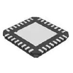


 工商网监
湘ICP备2023018690号
工商网监
湘ICP备2023018690号
