TSM104/A
QUAD OPERATIONAL AMPLIFIER AND
PROGRAMMABLE VOLTAGE REFERENCE
NOT FOR NEW DESIGN - REPLACED BY TSM104W
OPERATIONAL AMPLIFIERS
■ LOW SUPPLY CURRENT : 375µA/op.
(@ VCC = 5V)
■ LOW INPUT BIAS CURRENT : 20nA
■ MEDIUM SPEED : 0.9MHz
c
u
d
■ LOW INPUT OFFSET VOLTAGE : 0.5mV typ
N
DIP16
(Plastic Package)
for TSM104A
■ WIDE POWER SUPPLY RANGE : ±1.5V to
±15V
e
t
le
VOLTAGE REFERENCE
o
s
b
■ ADJUSTABLE OUTPUT VOLTAGE :
Vref to 36V
■ 0.4% AND 1% VOLTAGE PRECISION
s
(
t
c
DESCRIPTION
u
d
o
The TSM104 is a monolithic IC that includes four
op-amps and an adjustable shunt voltage reference. This device is offering space and cost saving in many applications like power supply management or data acquisition systems.
e
t
e
l
o
s
b
Pr
o
r
P
D
SO16
(Plastic Micropackage)
O
)
■ SINK CURRENT CAPABILITY : 1 to 100mA
■ TYPICAL OUTPUT IMPEDANCE : 0.2Ω
)
s
t(
ORDER CODE
Package
Part Number Temperature Range
TSM104I/AI
-40°C, +105°C
N
D
•
•
N = Dual in Line Package (DIP)
D = Small Outline Package (SO) - also available in Tape & Reel (DT)
PIN CONNECTIONS (top view)
O
Output 1
1
16
Output 4
2
15
Inverting Input
3
14
Non-inverting Input 4
V +
CC
4
13
V CC
Non-inverting Input 2
5
12
Non-inverting Input 3
Inverting Input 2
6
11
Inverting Input 3
Output 2
7
10
Output 3
Adjust
8
9
Cathode
Inverting Input 1
Non-inverting Input 1
January 2003
1/9
�TSM104/A
ABSOLUTE MAXIMUM RATINGS
Symbol
Parameter
VCC
Supply Voltage
Vid
Differential Input Voltage
Vi
Input Voltage
Value
Unit
36
V
36
V
-0.3 to 36
V
Output Short-circuit Duration
Toper
Tj
Rthja
Infinite
Operating Free-Air Temperature Range
-55 to +125
°C
Maximum Junction Temperature
150
°C
Thermal Resistance Junction to Ambient (SO package)
150
°C/W
)
s
t(
ELECTRICAL CHARACTERISTICS
VCC+ = 5V, V CC- = 0V, Tamb = 25°C (unless otherwise specified)
Symbol
ICC
Parameter
Min
Total Supply Current, excluding current in the Voltage
Reference
VCC+ = 5V, no load
Tmin. < Tamb < Tmax.
od
let
o
s
b
O
)
s
(
t
c
u
d
o
r
P
e
t
e
l
o
s
b
O
2/9
r
P
e
1.4
+
VCC = 30V, no load
Tmin. < Tamb < Tmax.
uc
Typ
Max
2.4
4
Unit
mA
�TSM104/A
ELECTRICAL CHARACTERISTICS
VCC+ = 5V, Vcc- = Ground, VO = 1.4V, Tamb = 25°C (unless otherwise specified)
Symbol
Vio
∆Vio
Iio
Iib
Avd
SVR
Vicm
CMR
Isource
Io
Isink
VOH
Parameter
s
b
O
SR
GBP
THD
1.
1
5
6
3
4
7
2
Unit
(s)
50
25
65
e
t
e
b
O
-
t
c
u
Low Level Output Voltage
RL = 10k
Tmin ≤ Tamb ≤ Tmax
Slew Rate at Unity Gain
Vi = 0.5 to 3V, VCC = 15V
RL = 2kΩ, CL = 100pF, unity gain
Gain Bandwith Product
VCC = 30V, RL = 2k, CL = 100pF
f = 100kHz, Vin = 10mV
Total Harmonic Distortion
f = 1kHz
AV = 20dB, RL = 2, VCC = 30V
CL = 100pF, Vo = 2Vpp
en
Equivalent Input Noise Voltage
f = 1kHz, VCC = 30V, Rs = 100Ω
Cs
Channel Separation
1kHz < f < 20kHz
l
o
s
0
0
µV/°C
nA
30
50
20
od
Pr
Max.
0.5
Large Signal Voltage Gain
VCC = 15V, RL = 2k
VO = 1.4V to 11.4V
Tmin ≤ Tamb ≤ Tmax
Supply Voltage Rejection Ratio
VCC = 5V to 30V
Input Voltage Mode Voltage Range
VCC = + 30V see note1)
Tmin ≤ Tamb ≤ Tmax
Common Mode Rejection Ratio
Tmin ≤ Tamb ≤ Tmax
Output Current Source
Vo = 2V, Vcc = +15V, Vid = +1V
Output Short Circuit to Ground
VCC = +15V
Output Current Sink
Vid = -1V
VCC = +15V, Vo = +2V
High Level Output Voltage
RL = 10k, VCC+ = 30V
Tamb = 25°C
Tmin ≤ Tamb ≤ Tmax
Typ.
mV
Input Offset Voltage Drift
Input Offset Current
Tmin ≤ Tamb ≤ Tmax
Input Bias Current
Tmin ≤ Tamb ≤ Tmax
e
t
e
ol
VOL
Min.
Input Offset Voltage
TSM104, Tamb = 25°C
Tmin ≤ Tamb ≤ Tmax
TSM104A, Tamb = 25°C
Tmin ≤ Tamb ≤ Tmax
150
200
)
s
t(
c
u
d
100
o
r
P
nA
V/mV
dB
100
70
60
85
20
40
Vcc+ -1.5
Vcc+-2
V
dB
mA
mA
40
10
60
20
mA
V
27
27
28
mV
5
20
20
V/µs
0.1
0.3
0.5
0.9
MHz
%
0.02
50
nV
-----------Hz
dB
120
The input common-mode voltage of either
input signal voltage should not be allowed to go negative by more than 0.3V. The upper end of the
common-mode voltage range is V CC+ -1.5V
But either of both inputs can go to +36V without damage.
3/9
But either of both inputs can go to +36V without damage
�TSM104/A
VOLTAGE REFERENCE
Symbol
Ik
Conditions
Cathode Current
Symbol
Vref
∆Vref
∆Vref
---------------∆V K A
Iref
Parameter
Reference Input Voltage
TSM104, Tamb = 25°C
Tmin ≤ Tamb ≤ Tmax
TSM104A, Tamb = 25°C
Tmin ≤ Tamb ≤ Tmax
Ratio of Change in Reference Input Voltage to Charge in
Cathode to Anode Voltage
IK = 10mA, ∆VKA =36V to 3V
Reference Input Current Deviation over T° Range
Imin
Minimum Cathode Current for Regulation
VKA = Vref
Ioff
Off-State Cathode Current
)
(s
ct
∆V
KA
1) The dynamic impedance is defined as ZKA = ---------------∆VI
s
b
O
4/9
Max
2.475
2.45
2.49
2.48
2.5
2.525
2.55
2.51
2.52
2.5
K
)
s
(
t
c
u
7
e
t
le
so
Ob
Dynamic Impedance - note 1
VKA = Vref , ∆IK = 1 to 100mA, f < 1kHz
e
t
e
ol
mA
Typ
-2
Reference Input Current
IK = 10mA
Tmin ≤ Tamb ≤ Tmax
o
r
P
1 to 100
Min
Reference Input Voltage Deviation Over Temperature Range
VKA = Vref , IK = 10mA
Tmin ≤ Tamb ≤ Tmax
du
Unit
Unit
V
∆Iref
ZKA
Value
30
od
Pr
mV
mV/V
-1.1
µA
1.5
2.5
3
0.8
1.2
µA
mA
0.5
1
180
500
nA
0.2
0.5
Ω
�TSM104/A
OPERATIONAL AMPLIFIERS
Unit Frequency = F(I)
Vcc=±15V, RL=2k, CL=100pF
1000
Unit Freq
Thousands
800
600
400
)
s
t(
200
0
-0.015
-0.01
-0.005
0
source sink
e
t
le
GBP = F(I)
c
u
d
0.01
0.015
o
r
P
o
s
b
Vcc=±15V, RL=2k, CL=100pF
O
)
600
s
(
t
c
400
u
d
o
200
r
P
e
0
-0.015
-0.01
let
o
s
b
O
-0.005
0
source sink
Phase and Gain Margin = F(I)
Phase Margin (deg)
Vcc=+/-15V, RL=2k, CL=100pF
60
0
50
-2
-4
40
-6
30
-8
20
-10
10
0
-0.015
Gain Margin (dB)
GBP
Thousands
800
-12
-0.01
-0.005
source sink
5/9
�TSM104/A
Total Harmonic Distorsion THD = F(freq)
0.014
THD(%)
0.012
0.01
0.008
)
s
t(
0.006
c
u
d
0.004
10
100
1000
Frequency (Hz)
e
t
le
10000
o
r
P
Noise = F(frequency)
o
s
b
Noise(nV/SQR(Hz))
80
O
)
60
u
d
o
20
r
P
e
t
e
l
o
s
b
O
6/9
s
(
t
c
40
0
0.01
0.1
1
Frequency (Hz)
10
100
�TSM104/A
VOLTAGE REFERENCE
Vref = F(Ik)
3
Vref (V)
2.5
2
1.5
)
s
t(
1
0.5
0.0001
0.001
uc
0.01
0.1
d
o
r
Cathode Current Ik (Amps)
P
e
Vref Stability = f(I,C)
t
e
l
o
s
b
O
)
(s
Current (Amps)
0.06
0.04
t
c
u
Unstable
0.02
d
o
r
P
e
let
o
s
b
Stable
0
1E-10
1E-9
1E-8
1E-7
1E-6
1E-5
Capacitor(F)
O
7/9
�TSM104/A
PACKAGE MECHANICAL DATA
16 PINS - PLASTIC PACKAGE
)
s
t(
c
u
d
e
t
le
Millimeters
Dim.
Min.
a1
B
b
b1
D
E
e
e3
F
i
L
Z
t
e
l
o
s
b
O
8/9
t
c
u
d
o
r
P
e
(s)
Typ.
0.51
0.77
o
s
b
-O
Inches
Max.
Min.
1.65
0.020
0.030
0.5
0.25
o
r
P
Typ.
Max.
0.065
0.020
0.010
20
8.5
2.54
17.78
0.787
0.335
0.100
0.700
7.1
5.1
3.3
0.280
0.201
0.130
1.27
0.050
�TSM104/A
PACKAGE MECHANICAL DATA
16 PINS - PLASTIC MICROPACKAGE (SO)
)
s
t(
c
u
d
e
t
le
Millimeters
Dim.
Min.
A
a1
a2
b
b1
C
c1
D
E
e
e3
F
G
L
M
S
O
od
r
P
e
t
e
l
o
bs
t
c
u
0.1
0.35
0.19
(s)
Typ.
o
s
b
-O
Max.
Inches
Min.
1.75
0.2
1.6
0.46
0.25
Typ.
Max.
0.069
0.008
0.063
0.018
0.010
0.004
0.014
0.007
0.5
0.020
45° (typ.)
9.8
5.8
10
6.2
0.386
0.228
1.27
8.89
3.8
4.6
0.5
o
r
P
0.394
0.244
0.050
0.350
4.0
5.3
1.27
0.62
0.150
0.181
0.020
0.157
0.209
0.050
0.024
8° (max.)
Information furnished is believed to be accurate and reliable. However, STMicroelectronics assumes no responsibility for the
consequences of use of such information nor for any infringement of patents or other rights of third parties which may result from
its use. No license is granted by implication or otherwise under any patent or patent rights of STMicroelectronics. Specifications
mentioned in this publication are subject to change without notice. This publication supersedes and replaces all information
previously supplied. STMicroelectronics products are not authorized for use as critical components in life support devices or
systems without express written approval of STMicroelectronics.
The ST logo is a registered trademark of STMicroelectronics
© 2003 STMicroelectronics - All Rights Reserved
STMicroelectronics GROUP OF COMPANIES
Australia - Brazil - China - Finland - France - Germany - Hong Kong - India - Italy - Japan - Malaysia - Malta - Morocco
Singapore - Spain - Sweden - Switzerland - United Kingdom
http://www.st.com
9/9
�
很抱歉,暂时无法提供与“TSM104IDT”相匹配的价格&库存,您可以联系我们找货
免费人工找货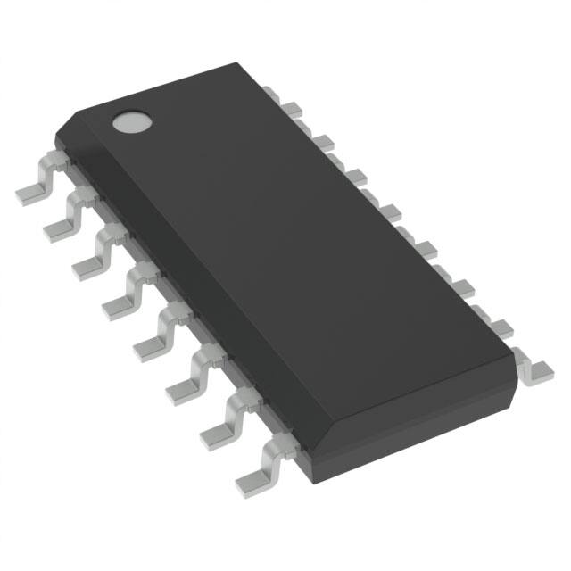


 工商网监
湘ICP备2023018690号
工商网监
湘ICP备2023018690号
