Notice for TAIYO YUDEN products
Please read this notice before using the TAIYO YUDEN products.
REMINDERS
■ Product information in this catalog is as of October 2014. All of the contents specified herein are subject to change
without notice due to technical improvements, etc. Therefore, please check for the latest information carefully before practical application or usage of the Products.
Please note that TAIYO YUDEN CO., LTD. shall not be responsible for any defects in products or equipment incorporating such products, which are caused under the conditions other than those specified in this catalog or individual specification.
■ Please contact TAIYO YUDEN CO., LTD. for further details of product specifications as the individual specification
is available.
■ Please conduct validation and verification of products in actual condition of mounting and operating environment
before commercial shipment of the equipment.
■ All electronic components or functional modules listed in this catalog are developed, designed and intended for
use in general electronics equipment.(for AV, office automation, household, office supply, information service,
telecommunications, (such as mobile phone or PC) etc.). Before incorporating the components or devices into any
equipment in the field such as transportation,( automotive control, train control, ship control), transportation signal,
disaster prevention, medical, public information network (telephone exchange, base station) etc. which may have
direct influence to harm or injure a human body, please contact TAIYO YUDEN CO., LTD. for more detail in advance.
Do not incorporate the products into any equipment in fields such as aerospace, aviation, nuclear control, submarine system, military, etc. where higher safety and reliability are especially required.
In addition, even electronic components or functional modules that are used for the general electronic equipment,
if the equipment or the electric circuit require high safety or reliability function or performances, a sufficient reliability evaluation check for safety shall be performed before commercial shipment and moreover, due consideration to
install a protective circuit is strongly recommended at customer's design stage.
■ The contents of this catalog are applicable to the products which are purchased from our sales offices or distributors (so called“TAIYO YUDEN’
s official sales channel”
).
It is only applicable to the products purchased from any of TAIYO YUDEN’s official sales channel.
■ Please note that TAIYO YUDEN CO., LTD. shall have no responsibility for any controversies or disputes that may
occur in connection with a third party's intellectual property rights and other related rights arising from your usage
of products in this catalog. TAIYO YUDEN CO., LTD. grants no license for such rights.
■ Caution for export
Certain items in this catalog may require specific procedures for export according to“Foreign Exchange and Foreign Trade Control Law”of Japan,“U.S. Export Administration Regulations”
, and other applicable regulations.
Should you have any question or inquiry on this matter, please contact our sales staff.
15
�SAW/FBAR DEVICES for MOBILE COMMUNICATIONS
REFLOW
■ ORDERING CODE
(A)
Previous Rule (applied to products registered on March 31, 2010 or before.)
F A R − D 6 N F − 1 G 9 6 0 0 − P 1 B Z − Z
❶
❷
❶Family
❸
❹
❷Common sign
−
Fixation
❺
❻
❼
❹Package type
❼Frequency
❺Product type
HIGH FREQUENCY PRODUCTS
❸Series
Product
Frequency Range
D5
Duplexer
700-1000MHz
D6
Duplexer
1000-5000MHz
700-1000MHz
J5 Dual Duplexers
F5
Device
700-1000MHz
F6
Device
1000-5000MHz
G5 Dual Devices
700-1000MHz
G6 Dual Devices
1000-5000MHz
❽
❾
❿
❽Common sign
−
Fixation
❻Common sign
−
Fixation
⓫
⓬
❿Serial Number
❾Design
⓫Custom, Status
⓬Packing
(B)
New Rule (applied to products registered on April 1, 2010 or later.)
D 6 N F 1 G 9 6 0 P 1 B Z − Z
❶
❷
❶Series
Product
Frequency Range
D5
Duplexer
700-1000MHz
D6
Duplexer
1000-5000MHz
J5 Dual Duplexers 700-1000MHz
F5
Device
700-1000MHz
F6
Device
1000-5000MHz
G5 Dual Devices
700-1000MHz
G6 Dual Devices 1000-5000MHz
❸
❹
❷Package type
❺
❹Frequency
❻
❺Design
❼
❽
❻Serial Number
❸Product type
❽Packing
❼Custom
*For further details, please contact to TAIYO YUDEN Co.,Ltd.
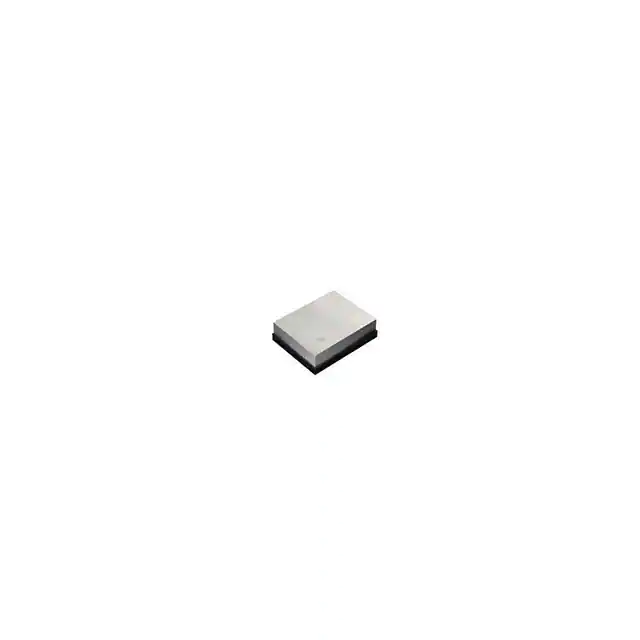
■ EXTERNAL DIMENSIONS/STANDARD QUANTITY
2.5×2.0×0.6
(8pin)
2.5×2.0×0.6
(9pin)
0.6max
2.5±0.1
2.5×2.0×0.65
0.6max
2.5±0.1
2.0±0.1
2.0±0.1
index
index
4-0.9625 2-0.3
0.9×0.375
4-0.7375
Unit:mm
1.4×1.0×0.5
1.40±0.1
Unit:mm
1.00±0.1
0.50
1.40±0.1
index
1.41
0.40
0.5
Unit:mm
0.25
0.25
0.575
0.25
1.00
0.25
Unit:mm
0.39
0.60
0.25
0.25
0.25
0.2
1.17
0.47
0.60
0.325
1.10±0.1
index
0.40
0.5max
1.50±0.1
0.5max
0.20
0.325
1.5×1.1×0.5
0.5max
0.90±0.1
0.25
Unit:mm
8-0.30
1.8×1.4×0.5
index
0.50
Unit:mm
8-0.425
1.80±0.1
1.10±0.1
index
C0.15
8-0.30
1.1×0.9×0.5
0.5max
0.60×0.30
4-0.575
8-0.375
8-0.425
2-0.325
C0.15
8-0.375
8-0.425
4-0.775
0.9×0.375
4-0.7375
C0.15
8-0.375
1.6±0.1
index
4-0.9625 2-0.3
C0.15
4-0.7375
0.5max
2.0±0.1
2.0±0.1
index
4-0.9625
2.0×1.6×0.5
0.65max
2.5±0.1
0.24 0.23
0.39
0.78
0.25
0.49
0.18
0.18
Unit:mm
0.18 0.21
0.21
Unit:mm
▶ This catalog contains the typical specification only due to the limitation of space. When you consider the purchase of our products, please check our specification.
For details of each product (characteristics graph, reliability information, precautions for use, and so on), see our Web site (http://www.ty-top.com/) .
136
15
�■ PART NUMBERS
●Duplexers
System
W-CDMA Band 1
PCS/W-CDMA Band 2
W-CDMA Band 4
CDMA/W-CDMA Band 5
W-CDMA Band 8
LTE Band 17
D6PE2G140P3AW
D6RB2G140E1AJ
FAR-D6NH-1G9600-M1Z9
FAR-D6NH-1G9600-M1Z6
FAR-D6NF-1G9600-P1BT
D6NF1G960P1BR
D6HH1G960BH95
D6PE1G960P3BY
D6PE2G132P3DWB
FAR-D5NG-881M50-M11Z
FAR-D5PF-881M50-M3E9
FAR-D5NE-881M50-P1A9
FAR-D5NE-881M50-P1A6Q
FAR-D5PE-881M50-P3EZ
FAR-D5PE-881M50-P3EY
D5NL881M5P1HY
FAR-D5NH-942M50-M1Y9
FAR-D5NF-942M50-P1GWQ
D5PF942M5M3G9
D5PE942M5P3GT
D5PE782M0M3P9
D5NL782M0P1JZ
Package Size
(mm)
2.0×1.6×0.5
1.8×1.4×0.5
2.5×2.0×0.65
2.5×2.0×0.65
2.5×2.0×0.65
2.5×2.0×0.65
2.5×2.0×0.65
2.0×1.6×0.57
2.0×1.6×0.5
2.5×2.0×0.6
2.0×1.6×0.5
2.5×2.0×0.6
2.5×2.0×0.6
2.0×1.6×0.5
2.0×1.6×0.5
3.0×2.5×0.7
2.5×2.0×0.65
2.5×2.0×0.65
2.0×1.6×0.5
2.0×1.6×0.5
2.0×1.6×0.5
3.0×2.5×0.7
Insertion Loss
(dB)
1.5/1.6
1.7/1.8
2.2/3.1
2.3/2.7
2.5/2.8
2.5/3.4
2.3/2.5
2.0/3.1
1.8/1.8
1.45/1.8
1.5/1.8
1.6/1.8
1.6/1.7
1.4/1.7
1.4/1.7
1.6/2.6
1.8/2.3
1.9/2.3
1.9/2.2
1.7/2.2
1.6/2.0
1.9/2.2
Isolation(dB)
Remarks
59/47
57/48
55/50
55/53
54/55
58/53
56/53
57/53
55/50
66/52
58/51
57/51
60/53
59/52
59/52
60/51
58/50
59/54
60/52
58/54
53/64
66/52
9 Pin, B Type Rx : Bal.100ohm
8 Pin, B Type Rx : Bal.100ohm
9 Pin, B Type
9 Pin, B Type Low Rx IL
9 Pin, B Type 100ohm, Low Rx IL
9 Pin, B Type Rx : Bal.100ohm High GPS Att. & Rx Isol.
9 Pin, B Type 100ohm
9 Pin, B Type Rx : Bal.100ohm
9 Pin, B Type Rx : Bal.100ohm
9 Pin, B Type
9 Pin, B Type
9 Pin, B Type Rx : Bal.100ohm
9 Pin, B Type 100ohm
9 Pin, B Type Rx : Bal.100ohm
9 Pin, A Type Rx : Bal.100ohm
SV-LTE
9 Pin, B Type
9 Pin, B Type 100ohm, GPS High Att.
9 Pin, B Type
9 Pin, B Type Rx : Bal.100ohm
9 Pin, B Type
SV-LTE
FAR-D5NE-740M00-P1C9
2.5×2.0×0.6
1.7/2.0
61/58
9 Pin, B Type Rx : Bal.100ohm
D5PE740M0P3NZ
2.0×1.6×0.5
1.9/2.0
63/60
9 Pin, B Type Rx : Bal.100ohm
LTE Band 20
D5NE847M0P1K9
2.5×2.0×0.6
2.1/2.3
52/51
9 Pin, B Type Rx : Bal.100ohm
LTE Band 21
D6PE1G503P3KW
2.0×1.6×0.5
1.6/2.0
55/56
9 Pin, B Type Rx : Bal.100ohm
LTE Band 26
LTE Band 28
CDMA BC0+BC10
D5PE876M5P3UZ
2.0×1.6×0.5
2.2/2.6
60/49
9 Pin, B Type Rx : Bal.100ohm
D5PF773M0M3Y6
2.0×1.6×0.5
1.8/2.3
60/53
Block A 9Pin, B Type
D5PF788M0M3Y9
2.0x1.6x0.5
1.8/2.4
60/54
Block B 9Pin, B Type
D5NF878M0P1ET
D5PE878M0P3UT
2.5×2.0×0.65
2.0×1.6×0.5
1.9/2.5
1.9/2.2
58/50
59/51
9 Pin, B Type Rx : Bal.100ohm
9 Pin, B Type Rx : Bal.100ohm
●CDMA/GSM850/Band 5
System
CDMA Tx
CDMA/GSM850 Tx
CDMA/W-CDMA Band 5 Rx
GSM850/CDMA Rx
GSM850 Rx
Part number
FAR-F5KB-836M50-B4ER
FAR-F5KB-836M50-B4EG
F5QA836M5M2AR
FAR-F5KA-836M50-D4DF
FAR-F5KB-881M50-B4ED
FAR-F5KY-881M50-B4UZ
FAR-F5KB-881M50-B4EJ
FAR-F5QB-881M50-P2BG
F5QG881M5P2KG
FAR-F5KA-881M50-D4DB
FAR-F5QA-881M50-M2AF
FAR-F5KB-881M50-B4EA
FAR-F5QB-881M50-P2BA
Package Size
(mm)
1.4×1.0×0.5
1.4×1.0×0.5
1.1×0.9×0.5
1.4×1.0×0.5
1.4×1.0×0.5
1.4×1.0×0.5
1.4×1.0×0.5
1.1×0.9×0.5
1.1×0.9×0.5
1.4×1.0×0.5
1.1×0.9×0.5
1.4×1.0×0.5
1.1×0.9×0.5
Insertion Loss
(dB)
1.7
1.6
1.9
1.9
1.5
1.5
1.4
1.5
1.5
1.7
1.6
1.7
1.3
Package Size
(mm)
1.4×1.0×0.5
1.4×1.0×0.5
1.4×1.0×0.5
Package Size
(mm)
1.4×1.0×0.5
1.4×1.0×0.5
1.1×0.9×0.5
1.4×1.0×0.5
1.4×1.0×0.5
1.4×1.0×0.5
1.1×0.9×0.5
1.4×1.0×0.5
1.4×1.0×0.5
1.1×0.9×0.5
Attenuation(dB)
Remarks
44
42
45
44
61
61
64
60
56
56
46
53
63
100ohm input
200ohm input
High Att.
High Att.
100ohm output
100ohm, High Att.
200ohm output
100ohm output
100ohm, High Att., Low Loss
High Att.
150ohm output
150ohm output
Insertion Loss
(dB)
2.3
1.4
2.1
Attenuation(dB)
Remarks
43
20
53
High Att.
Low IL
100ohm output
Insertion Loss
(dB)
2.2
2.6
2.3
2.0
1.6
2.4
1.6
1.9
2.0
2.2
Attenuation(dB)
Remarks
16
38
18
34
26
29
28
53
57
56
High Att.
High Att.
−
High Att.
150ohm output
100ohm output
150ohm output
High Att.
100ohm, High Att.
100ohm, High Att.
HIGH FREQUENCY PRODUCTS
LTE Band 13
Part number
●CDMA2000 BC0+BC10
System
CDMA2000 BC0+10 Tx
CDMA2000 BC0+10 Rx
Part number
F5KA833M0D4DU
F5KA833M0D4MG
F5KY878M0B4ND
●GSM/EGSM/Band 8
System
EGSM Tx
EGSM Rx
W-CDMA/LTE Band 8
Part number
FAR-F5KA-897M50-D4DC
FAR-F5KA-897M50-D4VW
F5QA897M5M2AC
FAR-F5KA-942M50-D4DD
FAR-F5KB-942M50-B4EB
FAR-F5KB-942M50-B4ES
FAR-F5QB-942M50-P2BB
F5KA942M5D4MYB
FAR-F5KY-942M50-B4UW
F5QG942M5P2KB
▶ This catalog contains the typical specification only due to the limitation of space. When you consider the purchase of our products, please check our specification.
For details of each product (characteristics graph, reliability information, precautions for use, and so on), see our Web site (http://www.ty-top.com/) .
15
137
�■ PART NUMBERS
●DCS/Band 3
Package Size
(mm)
1.4×1.0×0.5
1.1×0.9×0.5
1.4×1.0×0.5
1.4×1.0×0.5
1.1×0.9×0.5
1.1×0.9×0.5
1.4×1.0×0.5
Insertion Loss
(dB)
2.5
2.1
2.1
1.5
1.8
1.6
3.0
Attenuation(dB)
Remarks
30
22
20
14
15
17
50
150ohm output
100ohm
150ohm
100ohm, High Att.
Package Size
(mm)
1.4×1.0×0.5
1.4×1.0×0.5
1.1×0.9×0.5
1.4×1.0×0.5
1.4×1.0×0.5
1.4×1.0×0.5
1.4×1.0×0.5
1.1×0.9×0.5
1.4×1.0×0.5
1.4×1.0×0.5
1.1×0.9×0.5
Insertion Loss
(dB)
2.4
2.3
1.7
3.4
2.1
2.9
2.8
2.8
2.0
1.6
1.5
Attenuation(dB)
Remarks
35
28
20
43
23
49
50
44
18
18
15
High Att.
100ohm input
High Att.
100ohm output
100ohm, High Att.
100ohm output
100ohm output
Insertion Loss
(dB)
1.5/1.8
Attenuation(dB)
Remarks
FAR-G5QC-942M50-N2FB
Package Size
(mm)
1.5×1.1×0.5
50/29
GSM850 150ohm output EGSM 150ohm output
FAR-G5KT-942M50-Y4RW
1.8×1.4×0.5
1.9/2.2
50/25
GSM850 150ohm output EGSM 150ohm output
FAR-G5KW-942M50-Y4YD
1.8×1.4×0.5
2.5/1.8
32/38
EGSM 150ohm output GSM850 150ohm output
FAR-G5KC-942M50-Y4YW
FAR-G5QC-942M50-N2CD
FAR-G5KT-942M50-Y4RZ
FAR-G5QD-942M50-N2DB
FAR-G6QC-1G9600-N2FA
G6QJ1G960M2MB
1.8×1.4×0.5
1.5×1.1×0.5
1.8×1.4×0.5
1.5×1.1×0.5
1.5×1.1×0.5
1.5×1.1×0.5
1.8/1.4
1.7/1.4
2.2/1.9
2.5/2.0
1.9/1.7
1.9/1.9
31/54
29/51
25/52
25/55
17/13
19/19
EGSM 150ohm output GSM850 150ohm output
EGSM 150ohm output GSM850 150ohm output
EGSM 150ohm output GSM850 150ohm output
EGSM 150ohm output GSM850 150ohm output
DCS 150ohm output GSM1900 150ohm output
Rx Dual Unbal
FAR-G6KT-1G9600-Y4RU
1.8×1.4×0.5
1.8/2.0
18/13
DCS 150ohm output GSM1900 150ohm output
G6QD1G960N2DY
1.5×1.1×0.5
1.8/1.9
18/14
1 IN 4 OUT 150ohm output
GSM1900+DCS Rx
FAR-G6KC-1G9600-Y4YY
G6QC1G960N2CH
1.8×1.4×0.5
1.5×1.1×0.5
1.9/1.8
1.6/1.6
14/16
13/15
GSM1900 150ohm output DCS 150ohm output
GSM1900 150ohm output DCS 150ohm output
GSM1900+DCS Rx
(Common Input)
FAR-G6KT-1G9600-Y4RY
1.8×1.4×0.5
1.9/1.8
13/18
GSM1900 150ohm output DCS 150ohm output
FAR-G6KW-1G9600-Y4YC
G6QE1G960N2EC
G6QE1G960N2EE
G6QF1G960N2GA
1.8×1.4×0.5
1.5×1.1×0.5
1.5×1.1×0.5
1.5×1.1×0.5
2.2/3.1
2.5/2.5
2.2/2.2
1.6/1.4
13/15
18/13
31/14
14/54
170ohm output for IMC
GSM1900 150ohm output DCS 150ohm output
GSM1900/DCS 150ohm output Low Loss
GSM1900 150ohm output GSM850 150ohm output
Attenuation(dB)
Remarks
−
−
−
−
−
−
−
−
−
−
Low loss, High Att.
Low loss, High Att.
100ohm, Low loss
100ohm, High Att.
−
−
100ohm output
100ohm output
System
DCS Tx
DCS Rx
W-CDMA/LTE Band 3
Part number
FAR-F6KA-1G7475-D4CY
F6QA1G747M2QS
FAR-F6KA-1G8425-D4CK
FAR-F6KB-1G8425-B4GA
F6QB1G842P2BM
F6QB1G842P2BF
F6KY1G842B4UM
●PCS/GSM1900/Band 2
System
US-PCS Tx
US-PCS Rx
GSM1900/US-PCS Rx
HIGH FREQUENCY PRODUCTS
GSM1900 Rx
Part number
FAR-F6KA-1G8800-L4AF
FAR-F6KB-1G8800-B4GS
F6QA1G880M2AQ
FAR-F6KA-1G9600-D4MT
FAR-F6KB-1G9600-B4GP
FAR-F6KY-1G9600-B4UU
F6KY1G960B4NF
F6QG1G960P2KT
FAR-F6KA-1G9600-D4CR
FAR-F6KB-1G9600-B4GB
F6QB1G960P2BK
150ohm output
150ohm output
●GSM Dual
System
GSM850+EGSM Rx
GSM850+EGSM Rx
(Common Input)
GSM850+EGSM Rx
(Common Output)
EGSM+GSM850 Rx
EGSM+GSM850 Rx
(Common Input)
DCS+GSM1900 Rx
DCS+GSM1900 Rx
(Common Input)
DCS+GSM1900 Rx
(Common Input)
GSM1900+DCS Rx
(Common Output)
GSM1900+850 Rx
Part number
●GPS
System
GPS
GPS/GNSS
GPS+GLONASS+Galileo
+Compass
Part number
FAR-F6KA-1G5754-L4AJ
F6QA1G575H2JF
FAR-F6KB-1G5754-B4GE
FAR-F6KB-1G5754-B4GU
FAR-F6KA-1G5859-D4MS
F6QA1G585M2AT
FAR-F6KB-1G5859-B4HR
F6QB1G585P2BQ
F6KA1G581D4JR
F6QA1G581M2QZ
Package Size
(mm)
1.4×1.0×0.5
1.1×0.9×0.5
1.4×1.0×0.5
1.4×1.0×0.5
1.4×1.0×0.5
1.1×0.9×0.5
1.4×1.0×0.5
1.1×0.9×0.5
1.4×1.0×0.5
1.1×0.9×0.5
Insertion Loss
(dB)
0.9
0.96
1.1
1.2
1.0/1.2
1.1/1.4
1.1/1.4
1.5/1.7
1.6
1.1/1.4
▶ This catalog contains the typical specification only due to the limitation of space. When you consider the purchase of our products, please check our specification.
For details of each product (characteristics graph, reliability information, precautions for use, and so on), see our Web site (http://www.ty-top.com/) .
138
15
�■ PART NUMBERS
●W-CDMA
System
W-CDMA Band 1 Tx
W-CDMA Band 1 Rx
W-CDMA Band 1+2 Rx
W-CDMA Band 2+1 Rx
W-CDMA Band 4 Tx
W-CDMA Band 5+8 Rx
W-CDMA Band 8+5 Rx
(Common Output)
W-CDMA Band 7 Tx
W-CDMA/LTE Band 7 Rx
W-CDMA Band 9 Tx
W-CDMA Band 9 Rx
LTE Band 12 Tx
LTE Band 12 Rx
LTE Band 13 Rx
LTE Band 17 Tx
LTE Band 17 Rx
LTE Band 18 Tx
LTE Band 18+5 (BC0) Tx
LTE Band 20 Tx
LTE Band 20 Rx
LTE Band 21 Rx
LTE Band 25 Tx
LTE Band 26 Rx
LTE Band 28 Rx
LTE Band 29 Rx
TD LTE Bnad 38 Rx
TD LTE Band 38+40
(Common output)
TD LTE Band 40 Rx
FAR-F6KA-1G9500-D4DG
FAR-F6KB-1G9500-B4GJ
F6QA1G950M2AA
FAR-F6KA-2G1400-D4CG
FAR-F6KB-2G1400-B4GC
FAR-F6KA-2G1400-D4DW
FAR-F6KY-2G1400-B4UY
F6QG2G140P2KA
G6QL2G140M2PA
G6QH2G140N2LP
FAR-F6KA-1G7400-D4DE
G5QH942M5N2LN
Package Size
(mm)
1.4×1.0×0.5
1.4×1.0×0.5
1.1×0.9×0.5
1.4×1.0×0.5
1.4×1.0×0.5
1.4×1.0×0.5
1.4×1.0×0.5
1.1×0.9×0.5
1.5×1.1×0.5
1.5×1.1×0.5
1.4×1.0×0.5
1.5×1.1×0.5
Insertion Loss
(dB)
1.6
2.1
1.8
1.9
1.7
1.9
1.8
1.7
1.9/3.0
3.2/2.3
1.5
1.6/20
Attenuation(dB)
Remarks
38
34
38
39
39
48
64
55
48/41
53/54
44
56/50
Low loss, High Att.
100ohm output
Low loss, High Att.
100ohm output
High Att.
100ohm, High Att.
100ohm, High Att.
100ohm output
G5QT942M5N2VA
1.5×1.1×0.5
2.3/2.0
48/48
F6KA2G535L4AM
FAR-F6KY-2G6550-B4UN
F6QG2G655P2KE
FAR-F6KA-1G7675-D4CT
FAR-F6KB-1G8625-B4GT
F5KA707M5D4JW
F5KY737M0B4NN
FAR-F5KA-782M00-D4VP
F5QA782M0M2AZ
FAR-F5KY-751M00-B4UQ
F5QA751M0M2QM
FAR-F5KA-710M00-D4VQ
F5QA710M0M2AY
FAR-F5KY-740M00-B4UR
F5QG740M0P2KH
F5KA822M5D4VR
F5KA832M0D4JS
F5KA847M0D4ML
F5KY806M0B4NE
F5QA806M0M2QE
F6KY1G503B4NS
F6QA1G503M2QF
F6QA1G882M2AS
F5QG876M5P2KQ
F5QA773M0M2QC
F5QA788M0M2QB
F5BA722M5M6UW
F6KB2G595B4HS
1.4×1.0×0.5
1.4×1.0×0.5
1.1×0.9×0.5
1.4×1.0×0.5
1.4×1.0×0.5
1.4×1.0×0.5
1.4×1.0×0.5
1.4×1.0×0.5
1.1×0.9×0.5
1.4×1.0×0.5
1.1×0.9×0.5
1.4×1.0×0.5
1.1×0.9×0.5
1.4×1.0×0.5
1.1×0.9×0.5
1.1×0.9×0.5
1.4×1.0×0.5
1.4×1.0×0.5
1.4×1.0×0.5
1.1×0.9×0.5
1.4×1.0×0.5
1.1×0.9×0.5
1.1×0.9×0.5
1.1×0.9×0.5
1.1×0.9×0.5
1.1×0.9×0.5
1.1×0.9×0.5
1.4×1.0×0.5
1.6
2.8
2.5
1.8
2.1
1.6
1.4
1.5
1.5
1.6
1.9
1.2
1.3
1.4
1.4
1.6
1.5
1.7
2.5
2.7
1.4
2.0
1.8
2.2
2.1
2.0
1.6
2.6
30
54
52
31
40
23
57
55
56
50
50
32
33
60
65
40
19
52
45
41
47
52
23
59
52
52
38
−
2 (1.9G)100ohm out 1 (2G)100ohm out
100ohm output
100ohm. High Att.
100ohm. High Att.
Unbal.
100ohm output
Unbal.
100ohm output
Unbal.
100ohm output
Unbal.
Unbal.
100ohm output
100ohm output
Unbal.
Unbal.
100ohm output
Unbal.
100ohm output Low loss
Unbal.
Unbal.
100ohm output
Block A
Block B
Unbal.
150ohm output
G6QE2G595N2EJ
1.5×1.1×0.5
2.9/2.8
−
Balanced 100ohm
F6KB2G350B4HT
F6KB2G350B4HTB
1.4×1.0×0.5
1.4×1.0×0.5
2.7
2.5
−
−
150ohm output
Balanced 100ohm
Attenuation(dB)
Remarks
HIGH FREQUENCY PRODUCTS
LTE Band 13 Tx
Part number
●Other
System
Part number
ISM900 (B.W.26MHz)
TD-SCDMA/TD-LTE Band 34
TD-SCDMA/TD-LTE Band 39
FAR-F5QA-915M00-M2AK
FAR-F6KA-2G0175-D4DR
FAR-F6KA-1G9000-D4DS
G6QJ2G017M2MD
G6QJ2G017M2RD
TD-SCDMA Band 34+39
TD-SCDMA Band 39+34
(Common input)
TD-SCDMA Band 34+39
(Common input)
Wireless LAN
Package Size
(mm)
1.1×0.9×0.5
1.4×1.0×0.5
1.4×1.0×0.5
1.5×1.1×0.5
1.5×1.1×0.5
Insertion Loss
(dB)
1.8
1.8
1.6
1.3/1.4
1.6/2.0
−
−
−
−
−
High Att
2 IN/2 OUT
1 IN/2 OUT
G6QD2G017N2DU
1.5×1.1×0.5
1.7/2.0
−
Balanced 100ohm
G6QD2G017N2DC
1.5×1.1×0.5
2.2/1.8
−
Balanced 200ohm
FAR-F6KA-2G4418-D4CU
FAR-F6KA-2G4418-A4VA
FAR-F6KA-2G4500-A4VD
F6KA2G436A4VE
F6KA2G466A4VJ
1.4×1.0×0.5
1.4×1.0×0.5
1.4×1.0×0.5
1.4×1.0×0.5
1.4×1.0×0.5
2.6
3.0
1.9
2.5
2.8
−
−
−
−
−
+10dBm
+23dBm
Low IL,+19dBm
BW=72MHz,+24dBm
BW=68MHz,+24dBm
▶ This catalog contains the typical specification only due to the limitation of space. When you consider the purchase of our products, please check our specification.
For details of each product (characteristics graph, reliability information, precautions for use, and so on), see our Web site (http://www.ty-top.com/) .
15
139
�SAW/FBAR DEVICES (FILTER / DUPLEXERS)
■PACKAGING
①Minimum Quantity
Type
Duplexer
Single Filter
Dual Filter
Size(mm)
3.0×2.5
2.5×2.0
2.0×1.6
2.0×1.6
1.4×1.0
1.1×0.9
2.0×1.6
1.8×1.4
1.5×1.1
Z
Z
Z
Z
Z
3000
3000
3000
3000
3000
Z
Z
3000
3000
Code & Quantity(Pieces)
U
U
J
5000
J
5000
10000
10000
Y
Y
Y
Y
Y
Y
Y
15000
15000
15000
15000
15000
15000
15000
②Tape material
●Taping dimensions
Type
Duplexer
Single Filter
Dual Filter
Size(mm)
3.0×2.5
2.5×2.0
2.0×1.6
2.0×1.6
1.4×1.0
1.1×0.9
2.0×1.6
1.8×1.4
1.5×1.1
a
3.4±0.1
2.8±0.1
2.4±0.1
2.4±0.1
1.7±0.1
1.3±0.1
2.4±0.1
2.2±0.1
1.8±0.1
b
2.85±0.1
2.3±0.1
2.0±0.1
2.0±0.1
1.3±0.1
1.1±0.1
2.0
1.8
1.4
c
1.05±0.05
1.5+0.1/-0
1.05±0.05
1.05±0.05
0.5±0.05
0.5±0.05
1.05±0.05
0.5±0.05
0.5±0.05
d
1.55±0.05
1.5+0.1/-0
1.5+0.1/-0
1.5+0.1/-0
1.5+0.1/-0
1.55±0.05
1.5+0.1/-0
1.55±0.05
1.5+0.1/-0
e
1.0±0.1
1.0+0.1/-0.0
0.90-0.05
0.90-0.05
0.63±0.05
0.63±0.05
0.90-0.05
0.8±0.1
0.7±0.1
f
0.25±0.05
0.25±0.05
0.25±0.05
0.25±0.05
0.20±0.05
0.20±0.05
0.25±0.05
0.30±0.05
0.25±0.05
Unit:mm
●Material of Tape(Conductive)
Tape : Polystyrene
Top cover tape : Polyethylene terephthalate(PET)and Polyethylene
③Top Tape Strength
The top tape requires a peel-off force of 0.1 to 1.0N in the direction of the arrow as illustrated below.
▶ This catalog contains the typical specification only due to the limitation of space. When you consider the purchase of our products, please check our specification.
For details of each product (characteristics graph, reliability information, precautions for use, and so on), see our Web site (http://www.ty-top.com/) .
sawfilter_pack_e-E02R01
�④Reel size
●Material of Reel
Material : Polystyrene+Carbon
Characteristics : Conform to EIAJ-ET-7200A
Color : Black
Surface resistance(reference value) :109Ω/sq Max.
Code
Quantity
A
Z
3,000 pcs
φ180.0 +0.0/-1.5
J
5,000 pcs
φ180.0 +0.0/-1.5
U
10,000 pcs
φ330.0 ±2.0
Y
15,000 pcs
φ330.0 ±2.0
B
φ66.0 ±0.5
φ66.0 ±0.5
φ100.0 ±1.0
φ100.0 ±1.0
C
φ13.0 ±0.2
φ13.0 ±0.2
φ13.0 ±0.2
φ13.0 ±0.2
W1
9.0 +1.0/-0.0
9.0 +1.0/-0.0
9.4 ±1.0
9.4 ±1.0
W2
11.4 ±1.0
11.4 ±1.0
13.4 ±1.0
13.4 ±1.0
Unit:mm
⑤Reel label and Reel C-Label sticking and Winding method
●Surface
▶ This catalog contains the typical specification only due to the limitation of space. When you consider the purchase of our products, please check our specification.
For details of each product (characteristics graph, reliability information, precautions for use, and so on), see our Web site (http://www.ty-top.com/) .
sawfilter_pack_e-E02R01
�Filter
■RELIABILITY DATA
1. Terminal stregth
Specified Value
No damage to be found.
Bending Test.
according to IEC60068-2-21(JISC60068-2-21)
Test Methods and
Remarks
2. Mechanical shock
Specified Value
After testing, meet the specified characteristics at a room temperature.
Test Methods and
Remarks
Apply 14700m/s2 for 0.5ms 5 times for each of 6 directions.
according to IEC68-2-27(JISC60068-2-27).
3. Vibration
Specified Value
After testing, meet the specified characteristics at a room temperature.
Test Methods and
Remarks
With 1.5 mm of whole amplitude at 10 to 55 Hz of frequency, and 98m/s2 of acceleration at 55 to 500Hz, apply a
vibration for 2 hours for each of 3 directions, period is 15 minutes(10 to 500 to 10Hz)
4. Drop 1
Specified Value
After testing, meet the specified characteristics at a room temperature.
Test Methods and
Remarks
Drop 3 times onto concrete floor from the height of 1.0m.
5. Drop 2
Specified Value
After testing, meet the specified characteristics at a room temperature.
Test Methods and
Remarks
Drop with 150g weight 3 times in each 6 direction onto concrete floor from the height of 1.8m.
6. Temperature cycling
Specified Value
After testing, meet the specified characteristics at a room temperature.
Test Methods and
Remarks
Temp. range -40 to +100℃. 500cycle.
7. Static humidity
Specified Value
After testing, meet the specified characteristics at a room temperature.
Test Methods and
Remarks
+85℃, 90% to 95%RH, apply DC5V, 1000hours.
8. High temperature storage life
Specified Value
After testing, meet the specified characteristics at a room temperature.
Test Methods and
Remarks
+100℃, 1000hours.
9. Low temperature storage life
Specified Value
After testing, meet the specified characteristics at a room temperature.
Test Methods and
Remarks
-40℃, 1000hours.
▶ This catalog contains the typical specification only due to the limitation of space. When you consider the purchase of our products, please check our specification.
For details of each product (characteristics graph, reliability information, precautions for use, and so on), see our Web site (http://www.ty-top.com/) .
sawfilter_reli_e-E02R01
�10. Solderbility 1
Specified Value
More than 90% of area of terminals to be covered with the solder.
A change of the remarkable appearance do not have it.
Test Methods and
Remarks
Lead-free Solder paste, Reflow;Peak temperature 245℃
11. Solderbility 2
Specified Value
More than 90% of area of terminals to be covered with the solder.
A change of the remarkable appearance do not have it.
Test Methods and
Remarks
Sn-Pb Solder paste, Reflow;Peak temperature 235℃
12. Solder heat resistance
Specified Value
After testing, meet the specified characteristics at a room temperature.
A change of the remarkable appearance do not have it.
◆Recommended temperature profile of reflow soldering
Figure shows recommended temperature profile of reflow soldering in the case of lead-free solder alloy Sn3.0Ag0.5Cu.
Suitable condition for solder heating is differed depending on composition and manufacturing method.
Please contact to solder manufacturer for the details.
Test Methods and
Remarks
▶ This catalog contains the typical specification only due to the limitation of space. When you consider the purchase of our products, please check our specification.
For details of each product (characteristics graph, reliability information, precautions for use, and so on), see our Web site (http://www.ty-top.com/) .
sawfilter_reli_e-E02R01
�Duplexer
■RELIABILITY DATA
1. Terminal stregth
Specified Value
No damage to be found.
Bend width 4mm, hold for 5±1 sec.
according to IEC60068-2-21(JISC60068-2-21)
Test Methods and
Remarks
2. Mechanical shock
Specified Value
After testing, meet the specified characteristics at a room temperature.
Test Methods and
Remarks
Apply 14700m/s2 for 0.5ms 5 times for each of 6 directions.
according to IEC68-2-27(JISC60068-2-27).
3. Vibration
Specified Value
After testing, meet the specified characteristics at a room temperature.
Test Methods and
Remarks
With 1.5 mm of whole amplitude at 10 to 55 Hz of frequency, and 98m/s2 of acceleration at 55 to 500Hz, apply a
vibration for 2 hours for each of 3 directions, period is 15 minutes(10 to 500 to 10Hz)
4. Drop 1
Specified Value
After testing, meet the specified characteristics at a room temperature.
Test Methods and
Remarks
Drop 3 times onto concrete floor from the height of 1.0m.
5. Drop 2
Specified Value
After testing, meet the specified characteristics at a room temperature.
Test Methods and
Remarks
Drop with 150g weight 3 times in each 6 direction onto concrete floor from the height of 1.8m.
6. Temperature cycling
Specified Value
After testing, meet the specified characteristics at a room temperature.
Test Methods and
Remarks
Temp. range -40 to +100℃. 500cycle.
7. Static humidity
Specified Value
After testing, meet the specified characteristics at a room temperature.
Test Methods and
Remarks
+85℃, 90% to 95%RH, apply DC5V, 1000hours.
8. High temperature storage life
Specified Value
After testing, meet the specified characteristics at a room temperature.
Test Methods and
Remarks
+100℃, 1000hours.
9. Low temperature storage life
Specified Value
After testing, meet the specified characteristics at a room temperature.
Test Methods and
Remarks
-40℃, 1000hours.
▶ This catalog contains the typical specification only due to the limitation of space. When you consider the purchase of our products, please check our specification.
For details of each product (characteristics graph, reliability information, precautions for use, and so on), see our Web site (http://www.ty-top.com/) .
sawfilter_reli_e-E02R01
�10. High Temperature Bias
Specified Value
After testing, meet the specified characteristics at a room temperature.
Test Methods and
Remarks
+50℃, +29dBm, 50000hours.
11. Solderbility 1
Specified Value
More than 90% of area of terminals to be covered with the solder.
A change of the remarkable appearance do not have it.
Test Methods and
Remarks
Lead-free Solder paste, Reflow;Peak temperature 245℃
12. Solderbility 2
Specified Value
More than 90% of area of terminals to be covered with the solder.
A change of the remarkable appearance do not have it.
Test Methods and
Remarks
Sn-Pb Solder paste, Reflow;Peak temperature 235℃
13. Solder heat resistance
Specified Value
After testing, meet the specified characteristics at a room temperature.
A change of the remarkable appearance do not have it.
◆Recommended temperature profile of reflow soldering
Figure shows recommended temperature profile of reflow soldering in the case of lead-free solder alloy Sn3.0Ag0.5Cu.
Suitable condition for solder heating is differed depending on composition and manufacturing method.
Please contact to solder manufacturer for the details.
Test Methods and
Remarks
▶ This catalog contains the typical specification only due to the limitation of space. When you consider the purchase of our products, please check our specification.
For details of each product (characteristics graph, reliability information, precautions for use, and so on), see our Web site (http://www.ty-top.com/) .
sawfilter_reli_e-E02R01
�


 工商网监
湘ICP备2023018690号
工商网监
湘ICP备2023018690号
