TAK CHEONG
®
SEM I COND U CTO R
Plastic Package
N-Channel MOSFET
Absolute Maximum Ratings
Green Product
3
TA = 25°C unless otherwise noted
Parameter
Symbol
2N7002T
150mW SOT-523 SURFACE MOUNT
Value
Units
60
V
±20V
V
2
VDS
Drain-Source Voltage
VGS
Continuous Gate-Source Voltage
ID
Continuous Drain Current
115
mA
PD
Power Dissipation
150
mW
RθJA
Thermal Resistance from Junction to Ambient
833
°C /W
TSTG
Storage Temperature Range
-55 to +150
°C
+150
°C
TJ
Operating Junction Temperature
1. Gate
2. Source
3. Drain
1
SOT-523
These ratings are limiting values above which the serviceability of the device may be impaired.
Specification Features:
§
Low On-resistance
§
Low Gate Threshold Voltage
§
Low Input capacitance
§
RoHS Compliant
§
Green EMC
§
Matte Tin(Sn) Lead Finish
§
Weight: approx. 0.002g
Electrical Symbol:
Device Marking Code:
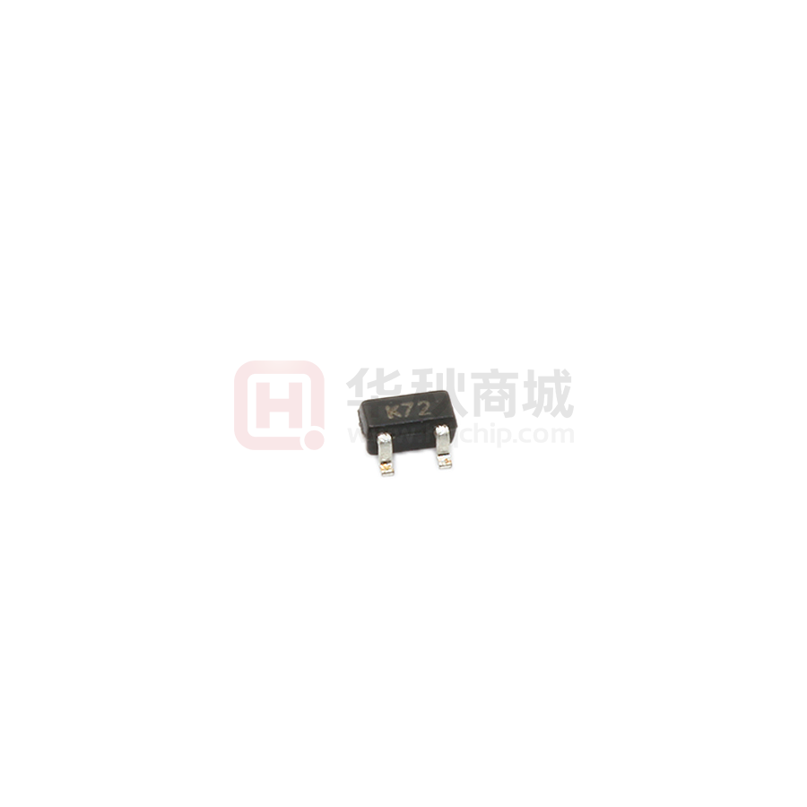
K72
DB Number: DB-246
July 2018, Revision B
Page 1
�TAK CHEONG
®
SEM I COND U CTO R
Electrical Characteristics (TA = 25°C unless otherwise noted)
Off Characteristics
Parameter
Symbol
BVDSS
Test Condition
Limits
Min
Typ
Max
60
Unit
Drain-Source Breakdown Voltage
VGS=0V, ID=10uA
Volts
IGSS
Gate-Body Leakage
VDS=0V, VGS=±20V
±1
uA
IDSS
Zero Gate Voltage Drain Current
VDS=60V, VGS=0V
100
nA
On Characteristics
Parameter
Symbol
Test Condition
Limits
Min
Typ
Max
Unit
Vth(GS)
Gate-Threshold Voltage
VDS= VGS, ID=250uA
ID(ON)
On-state Drain Current
VGS=10V, VDS=7V
Drain-Source On-Resistance
VGS=10V, ID=500mA
7.5
Ω
VGS=5V, ID=50mA
7.5
Ω
500
ms
RDS(on)
gfs
VDS(on)
VSD
1
2.5
500
Volts
mA
Forward Trans Conductance
VDS=10V, ID=200mA
Drain-Source On-Voltage
VGS=10V, ID=500mA
3.75
V
VGS=5V, ID=50mA
0.375
V
IS=250mA, VGS=0V
1
V
Diode Forward Voltage
80
Dynamic Characteristics
Symbol
Ciss
Parameter
Test Condition
Input Capacitance
Coss
Output Capacitance
Crss
Reverse Transfer Capacitance
VDS = 25V, VGS = 0V,
f = 1.0MHz
Limits
Unit
Min
Typ
Max
--
--
50
pF
--
--
25
pF
--
--
5.0
pF
Switching Characteristics
Parameter
Symbol
tD(on)
tD(off)
Turn-on Time
Test Condition
VDD=10V, RL=20Ω,
Limits
Unit
Min
Typ
Max
--
5.6
--
nS
--
25
--
nS
ID=500mA, VGEN=10V,
Turn-off Time
RG = 10Ω
DB Number: DB-246
July 2018, Revision B
Page 2
�TAK CHEONG
®
SEM I COND U CTO R
SOT-523 Package Outline
MILLIMETERS
INCHES
DIM
Typical Soldering Pattern:
MIN
MAX
MIN
MAX
A
0.70
0.90
0.028
0.035
A1
0.00
0.10
0.000
0.004
A2
0.70
0.80
0.028
0.031
b1
0.15
0.25
0.006
0.010
b2
0.25
0.35
0.010
0.014
c
0.10
0.20
0.004
0.008
D
1.50
1.70
0.059
0.067
E
0.70
0.90
0.028
0.035
E1
1.45
1.75
0.057
0.069
e
e1
0.50 TYP.
0.90
L
L1
θ
0.020 TYP.
1.10
0.035
0.40 REF.
0.10
O
0
0.043
0.016 REF.
0.30
O
8
0.004
O
0
0.012
8O
NOTES:
1. Above package outline conforms to JEITA EAIJ ED-7500A SC-75A.
2. Dimensions are exclusive of Burrs, Mold Flash & Tie Bar extrusions.
DB Number: DB-246
July 2018, Revision B
Page 3
�TAK CHEONG
®
DISC LA I MER NOTIC E
NOTICE
The information presented in this document is for reference only. Tak Cheong reserves the right to make
changes without notice for the specification of the products displayed herein.
The product listed herein is designed to be used with ordinary electronic equipment or devices, and not
designed to be used with equipment or devices which require high level of reliability and the malfunction of with
would directly endanger human life (such as medical instruments, transportation equipment, aerospace
machinery, nuclear-reactor controllers, fuel controllers and other safety devices), Tak Cheong Semiconductor
Co., Ltd., or anyone on its behalf, assumes no responsibility or liability for any damagers resulting from such
improper use of sale.
This publication supersedes & replaces all information reviously supplied. For additional information, please visit
our website http://www.takcheong.com, or consult your nearest Tak Cheong’s sales office for further assistance.
Number: DB-100
April 14, 2008 / A
�
很抱歉,暂时无法提供与“2N7002T”相匹配的价格&库存,您可以联系我们找货
免费人工找货- 国内价格
- 10+0.11521
- 50+0.10657
- 200+0.09937
- 600+0.09217
- 1500+0.08640
- 3000+0.08280


 工商网监
湘ICP备2023018690号
工商网监
湘ICP备2023018690号
