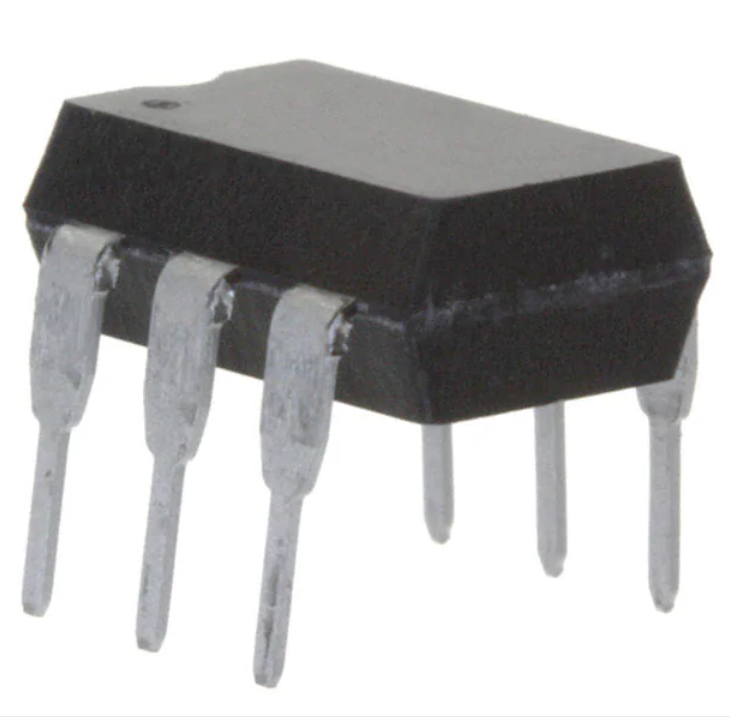
4N32, 4N33
www.vishay.com
Vishay Semiconductors
Optocoupler, Photodarlington Output, High Gain,
With Base Connection
FEATURES
A
1
6 B
C
2
5 C
NC
3
4 E
• Very high current transfer ratio, 500 % min.
• High isolation resistance, 1011 Ω typical
• Standard plastic DIP package
• Material categorization:
for definitions of compliance please see
www.vishay.com/doc?99912
i179005_1
V
D E
i179005
AGENCY APPROVALS
• UL1577, file no. E52744 system code H
DESCRIPTION
• DIN EN 60747-5-2 (VDE 0884) / DIN EN 60747-5-5
(pending), available with option 1
The 4N32 and 4N33 are optically coupled isolators with a
gallium arsenide infrared LED and a solicon photodarlington
sensor.
• BSI IEC 60950; IEC 60065
• FIMKO
Switching can be achieved while maintaining a high degree
of isolation between driving and load circuits.
These optocouplers can be used to replace reed and
mercury relays with advantages of long life, high speed
switching and elimination of magnetic fields.
ORDERING INFORMATION
4
N
3
#
PART NUMBER
-
X
0
#
PACKAGE OPTION
AGENCY CERTIFIED/PACKAGE
#
DIP
T
TAPE AND
REEL
7.62 mm
CTR (%)
UL, BSI, FIMKO
≥ 500
≥ 500
DIP-6
4N32
4N33
Note
• Additional options may be possible, please contact sales office
Rev. 1.3, 30-Nov-17
Document Number: 81865
1
For technical questions, contact: optocoupleranswers@vishay.com
THIS DOCUMENT IS SUBJECT TO CHANGE WITHOUT NOTICE. THE PRODUCTS DESCRIBED HEREIN AND THIS DOCUMENT
ARE SUBJECT TO SPECIFIC DISCLAIMERS, SET FORTH AT www.vishay.com/doc?91000
�4N32, 4N33
www.vishay.com
Vishay Semiconductors
ABSOLUTE MAXIMUM RATINGS (Tamb = 25 °C, unless otherwise specified)
PARAMETER
TEST CONDITION
SYMBOL
VALUE
UNIT
input
Reverse voltage
VR
3
V
Forward current
IF
60
mA
Power dissipation
Derate linearly
Pdiss
From 55 °C
100
mW
1.33
mW/°C
output
Collector emitter breakdown voltage
BVCEO
30
V
Emitter base breakdown voltage
BVEBO
8
V
Collector base breakdown voltage
BVCBO
50
V
Emitter collector breakdown voltage
BVECO
5
V
IC
100
mA
Pdiss
150
mW
2
mW/°C
Collector (load) current
Power dissipation
Derate linearly
coupler
Total dissipation
Ptot
250
mW
3.3
mW/°C
Derate linearly
Isolation test voltage (between emitter
1s
VISO
5300
VRMS
7
mm min.
Leakage path
Air path
Isolation resistance
7
mm min.
VIO = 500 V, Tamb = 25 °C
RIO
≥ 1012
Ω
VIO = 500 V, Tamb = 100 °C
RIO
≥ 1011
Ω
Tstg
-55 to +150
°C
Tamb
-55 to +100
°C
10
s
Storage temperature
Operating temperature
Lead soldering time (1)
At 260 °C
Notes
• Stresses in excess of the absolute maximum ratings can cause permanent damage to the device. Functional operation of the device is not
implied at these or any other conditions in excess of those given in the operational sections of this document. Exposure to absolute
maximum ratings for extended periods of the time can adversely affect reliability
(1) Refer to reflow profile for soldering conditions for surface mounted devices (SMD). Refer to wave profile for soldering conditions for through
hole devices (DIP)
ELECTRICAL CHARACTERISTICS (Tamb = 25 °C, unless otherwise specified)
PARAMETER
TEST CONDITION
SYMBOL
MIN.
TYP.
MAX.
UNIT
input
Forward voltage
IF = 50 mA
VF
-
1.25
1.5
V
Reverse current
VR = 3 V
IR
-
0.1
100
μA
Capacitance
VR = 0 V
CO
-
25
pF
output
Collector emitter breakdown voltage (1)
IC = 100 μA, IF = 0
BVCEO
30
-
-
V
Collector base breakdown voltage (1)
IC = 100 μA, IF = 0
BVCBO
50
-
-
V
Emitter base breakdown voltage (1)
IC = 100 μA, IF = 0
BVEBO
8
-
-
V
Emitter collector breakdown voltage (1)
IC = 100 μA, IF = 0
BVECO
5
10
-
V
VCE = 10 V, IF = 0
ICEO
-
1
100
nA
IC = 0.5 mA, VCE = 5 V
hFE
13
-
-
VCEsat
-
1
-
V
-
1.5
-
pF
Collector emitter leakage current
coupler
Collector emitter saturation voltage
Coupling capacitance
Notes
• Minimum and maximum values are testing requirements. Typical values are characteristics of the device and are the result of engineering
evaluation. Typical values are for information only and are not part of the testing requirements
(1) Indicates JEDEC® registered values
Rev. 1.3, 30-Nov-17
Document Number: 81865
2
For technical questions, contact: optocoupleranswers@vishay.com
THIS DOCUMENT IS SUBJECT TO CHANGE WITHOUT NOTICE. THE PRODUCTS DESCRIBED HEREIN AND THIS DOCUMENT
ARE SUBJECT TO SPECIFIC DISCLAIMERS, SET FORTH AT www.vishay.com/doc?91000
�4N32, 4N33
www.vishay.com
Vishay Semiconductors
CURRENT TRANSFER RATIO
PARAMETER
Current transfer ratio
TEST CONDITION
SYMBOL
MIN.
TYP.
MAX.
UNIT
VCE = 10 V, IF = 10 mA
CTR
500
-
-
%
SWITCHING CHARACTERISTICS
PARAMETER
TEST CONDITION
SYMBOL
MIN.
TYP.
MAX.
UNIT
Turn-on time
VCC = 10 V, IC = 50 mA
ton
-
-
5
μs
Turn-off time
IF = 200 mA, RL = 180 Ω
toff
-
-
100
μs
SYMBOL
MIN.
TYP.
MAX.
UNIT
-
55 / 100 / 21
-
SAFETY AND INSULATION RATINGS
PARAMETER
TEST CONDITION
Climatic classification
According to IEC 68 part 1
Comparative tracking index
175
-
399
VIOTM
CTI
8000
-
-
VIORM
V
890
-
-
V
PSO
-
-
700
mW
ISI
-
-
400
mA
TSI
-
-
175
°C
7
-
-
mm
Standard DIP-6
7
-
-
mm
Per IEC 60950 2.10.5.1
0.4
-
-
mm
Creepage distance
Standard DIP-6
Clearance distance
Insulation thickness, reinforced rated
Note
• As per IEC 60747-5-2, § 7.4.3.8.1, this optocoupler is suitable for “safe electrical insulation” only within the safety ratings. Compliance with
the safety ratings shall be ensured by means of protective circuits
TYPICAL CHARACTERISTICS (Tamb = 25 °C, unless otherwise specified)
10
1.0
Normalized to:
VCE = 5 V
IF = 10 mA
0.8
TA = 25 °C
VCE = 5 V
0.6
0.4
NICE - Normalized ICE
NCTRCE - Normalized CTRCE
1.2
Normalized to:
VCE = 5 V
1 IF = 10 mA
VCE = 5 V
TA = 25 °C
VCE = 1 V
0.1
0.01
0.2
VCE = 1 V
0.0
0.1
i4n32-33_02
1
10
100
1000
IF - LED Current (mA)
Fig. 1 - Normalized Non-Saturated and Saturated CTRCE vs.
LED Current
Rev. 1.3, 30-Nov-17
0.001
0.1
i4n32-33_03
1
10
100
IF - LED Current (mA)
Fig. 2 - Normalized Non-Saturated and Saturated Collector Emitter
Current vs. LED Current
Document Number: 81865
3
For technical questions, contact: optocoupleranswers@vishay.com
THIS DOCUMENT IS SUBJECT TO CHANGE WITHOUT NOTICE. THE PRODUCTS DESCRIBED HEREIN AND THIS DOCUMENT
ARE SUBJECT TO SPECIFIC DISCLAIMERS, SET FORTH AT www.vishay.com/doc?91000
�4N32, 4N33
www.vishay.com
Vishay Semiconductors
20
10
tpHL - High/Low Propagation
Delay (µs)
NICB - Normalized ICB
Normalized to:
VCB = 3.5 V
1
IF = 10 mA
TA = 25 °C
0.1
0.01
0.001
0.1
1
10
TA = 25 °C
VCC = 5 V
VTH = 1.5 V
10
100 Ω
5
0
100
0
IF = LED Current (mA)
i4n32-33_04
1 kΩ
15
i4n32-33_07
10
5
15
20
IF - LED Current (mA)
Fig. 6 - High to Low Propagation Delay vs.
Collector Load Resistance and LED Current
Fig. 3 - Normalized Collector Base Photocurrent vs.
LED Current
10 000
hFE - Forward Transfer Gain
TA = 25 °C
VCE = 5 V
8000
IF
VCC
RL
6000
VO
4000
tD
tR
VO
tPLH
IF
VCE = 1 V
VTH = 1.5 V
2000
tPHL
0
0.01
0.1
1
10
100
tS
tF
i4n32-33_08
Ib - Base Current (µA)
i4n32-33_05
Fig. 4 - Non-Saturated and Saturated hFE vs.
Base Current
Fig. 7 - Switching Waveform and Switching Schematic
tpLH - Low/High Propagation
Delay (µs)
80
TA = 25 °C, VCC = 5 V
VTH = 1.5 V
1 kΩ
60
220 Ω
40
470 Ω
20
100 Ω
0
0
i4n32-33_06
5
10
15
20
IF - LED Current (mA)
Fig. 5 - Low to High Propagation Delay vs.
Collector Load Resistance and LED Current
Rev. 1.3, 30-Nov-17
Document Number: 81865
4
For technical questions, contact: optocoupleranswers@vishay.com
THIS DOCUMENT IS SUBJECT TO CHANGE WITHOUT NOTICE. THE PRODUCTS DESCRIBED HEREIN AND THIS DOCUMENT
ARE SUBJECT TO SPECIFIC DISCLAIMERS, SET FORTH AT www.vishay.com/doc?91000
�4N32, 4N33
www.vishay.com
Vishay Semiconductors
PACKAGE DIMENSIONS in millimeters
DIP-6 Package Dimensions
3
2
1
4
5
6
Pin one ID
6.4 ± 0.1
ISO method A
8.6 ± 0.1
1 min.
7.62 typ.
1.2 ± 0.1
3.555 ± 0.255
18°
4° typ.
2.95 ± 0.5
0.8 min.
0.85 ± 0.05
0.5 ± 0.05
3° to 9°
0.25 typ.
7.62 to 8.81
i178004
2.54 typ.
PACKAGE MARKING
4N32
V YWW H 68
Notes
• Example marking for 4N32
• Only options 1, and 7 reflected in the package marking
• The VDE logo is only marked on option 1 parts
• Tape and reel suffix (T) is not part of the package marking
Rev. 1.3, 30-Nov-17
Document Number: 81865
5
For technical questions, contact: optocoupleranswers@vishay.com
THIS DOCUMENT IS SUBJECT TO CHANGE WITHOUT NOTICE. THE PRODUCTS DESCRIBED HEREIN AND THIS DOCUMENT
ARE SUBJECT TO SPECIFIC DISCLAIMERS, SET FORTH AT www.vishay.com/doc?91000
�Legal Disclaimer Notice
www.vishay.com
Vishay
Disclaimer
ALL PRODUCT, PRODUCT SPECIFICATIONS AND DATA ARE SUBJECT TO CHANGE WITHOUT NOTICE TO IMPROVE
RELIABILITY, FUNCTION OR DESIGN OR OTHERWISE.
Vishay Intertechnology, Inc., its affiliates, agents, and employees, and all persons acting on its or their behalf (collectively,
“Vishay”), disclaim any and all liability for any errors, inaccuracies or incompleteness contained in any datasheet or in any other
disclosure relating to any product.
Vishay makes no warranty, representation or guarantee regarding the suitability of the products for any particular purpose or
the continuing production of any product. To the maximum extent permitted by applicable law, Vishay disclaims (i) any and all
liability arising out of the application or use of any product, (ii) any and all liability, including without limitation special,
consequential or incidental damages, and (iii) any and all implied warranties, including warranties of fitness for particular
purpose, non-infringement and merchantability.
Statements regarding the suitability of products for certain types of applications are based on Vishay's knowledge of typical
requirements that are often placed on Vishay products in generic applications. Such statements are not binding statements
about the suitability of products for a particular application. It is the customer's responsibility to validate that a particular product
with the properties described in the product specification is suitable for use in a particular application. Parameters provided in
datasheets and / or specifications may vary in different applications and performance may vary over time. All operating
parameters, including typical parameters, must be validated for each customer application by the customer's technical experts.
Product specifications do not expand or otherwise modify Vishay's terms and conditions of purchase, including but not limited
to the warranty expressed therein.
Hyperlinks included in this datasheet may direct users to third-party websites. These links are provided as a convenience and
for informational purposes only. Inclusion of these hyperlinks does not constitute an endorsement or an approval by Vishay of
any of the products, services or opinions of the corporation, organization or individual associated with the third-party website.
Vishay disclaims any and all liability and bears no responsibility for the accuracy, legality or content of the third-party website
or for that of subsequent links.
Except as expressly indicated in writing, Vishay products are not designed for use in medical, life-saving, or life-sustaining
applications or for any other application in which the failure of the Vishay product could result in personal injury or death.
Customers using or selling Vishay products not expressly indicated for use in such applications do so at their own risk. Please
contact authorized Vishay personnel to obtain written terms and conditions regarding products designed for such applications.
No license, express or implied, by estoppel or otherwise, to any intellectual property rights is granted by this document or by
any conduct of Vishay. Product names and markings noted herein may be trademarks of their respective owners.
© 2022 VISHAY INTERTECHNOLOGY, INC. ALL RIGHTS RESERVED
Revision: 01-Jan-2022
1
Document Number: 91000
�


 工商网监
湘ICP备2023018690号
工商网监
湘ICP备2023018690号


