6N137, VO2601, VO2611, VO2630, VO2631, VO4661
www.vishay.com
Vishay Semiconductors
High Speed Optocoupler, Single and Dual, 10 MBd
FEATURES
Single channel
NC 1
• Choice of CMR performance of 15 kV/μs,
5 kV/μs, and 1000 V/μs
• High speed: 10 MBd typical
• +5 V CMOS compatibility
8 V
CC
A 2
7 V
E
C 3
6 VO
NC 4
5 GND
• Pure tin leads
• Guaranteed AC and DC performance over
temperature
• Meets IEC 60068-2-42 (SO2) and IEC 60068-2-43 (H2S)
requirements
• Low input current capability of 5 mA
• Material categorization: for definitions of compliance
please see www.vishay.com/doc?99912
6N137, VO2601, VO2611
Dual channel
A1 1
8 VCC
C1 2
7 V
O1
C2 3
6 V
O2
4
A2
5 GND
VO2630, VO2631, VO4661
APPLICATIONS
•
•
•
•
LINKS TO ADDITIONAL RESOURCES
3D 3D
3D Models
Design Tools
Related
Documents
•
•
•
•
•
DESCRIPTION
The 6N137, VO2601, and VO2611 are single channel
10 MBd optocouplers utilizing a high efficient input LED
coupled with an integrated optical photodiode IC detector.
The detector has an open drain NMOS-transistor output,
providing less leakage compared to an open collector
Schottky clamped transistor output. The VO2630, VO2631,
and VO4661 are dual channel 10 MBd optocouplers. For the
single channel type, an enable function on pin 7 allows the
detector to be strobed. The internal shield provides a
guaranteed common mode transient immunity of 5 kV/μs for
the VO2601 and VO2631 and 15 kV/μs for the VO2611 and
VO4661. The use of a 0.1 μF bypass capacitor connected
between pin 5 and 8 is recommended.
Microprocessor system interface
PLC, ATE input / output isolation
Computer peripheral interface
Digital fieldbus isolation: CC-link, DeviceNet, profibus,
SDS
High speed A/D and D/A conversion
AC plasma display panel level shifting
Multiplexed data transmission
Digital control power supply
Ground loop elimination, noise isolation
AGENCY APPROVALS
•
•
•
•
•
UL1577
cUL
DIN EN 60747-5-5 (VDE 0884-5) available with option 1
CQC GB8898-2011
CQC GB4943.1-2011
ORDERING INFORMATION
V
O
2
6
0
1
PART NUMBER
Rev. 2.1, 15-Jan-2021
X
0
#
PACKAGE OPTION
AGENCY CERTIFIED /
PACKAGE
UL, cUL, CQC
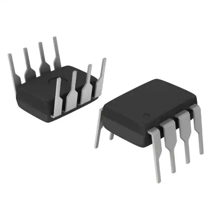
DIP-8
DIP-8, 400 mil (option 6)
SMD-8 (option 7)
SMD-8 (option 9)
VDE, UL, cUL, CQC
DIP-8, 400 mil (option 6)
SMD-8 (option 7)
-
1000
6N137
6N137-X006
6N137-X007T
6N137-X009T
1000
-
#
DIP-8
Option 6
7.62 mm
10.16 mm
T
TAPE
AND
REEL
Option 7
> 0.7 mm
Option 9
> 0.1 mm
CHANNELS 1
CHANNELS 2
CMR (V/μs)
CMR (V/μs)
5000
15 000
1000
5000
15 000
VO2601
VO2611
VO2630
VO2631
VO4661
VO2601-X006 VO2611-X006
VO2631-X006 VO4661-X006
VO2601-X007T VO2611-X007T VO2630-X007T VO2631-X007T VO4661-X007T
VO2630-X009T
5000
15 000
1000
5000
15 000
VO2611-X016
VO2601-X017T VO2611-X017T
VO2631-X017T
-
Document Number: 84732
1
For technical questions, contact: optocoupleranswers@vishay.com
THIS DOCUMENT IS SUBJECT TO CHANGE WITHOUT NOTICE. THE PRODUCTS DESCRIBED HEREIN AND THIS DOCUMENT
ARE SUBJECT TO SPECIFIC DISCLAIMERS, SET FORTH AT www.vishay.com/doc?91000
�6N137, VO2601, VO2611, VO2630, VO2631, VO4661
www.vishay.com
Vishay Semiconductors
TRUTH TABLE (positive logic)
LED
ENABLE
OUTPUT
On
H
L
Off
H
H
On
L
H
Off
L
H
On
NC
L
Off
NC
H
ABSOLUTE MAXIMUM RATINGS (Tamb = 25 °C, unless otherwise specified)
PARAMETER
CONDITIONS
SYMBOL
VALUE
UNIT
Average forward current (single channel)
IF
20
mA
Average forward current
(per channel for dual channel)
IF
15
mA
Reverse input voltage
VR
5
V
Enable input voltage
VE
VCC + 0.5 V
V
INPUT
Enable input current
IE
5
mA
IFSM
200
mA
Output power dissipation
(single channel)
Pdiss
35
mW
Output power dissipation (per channel for
dual channel)
Pdiss
25
mW
Surge current
t = 100 μs
OUTPUT
Supply voltage
1 min maximum
Output current
Output voltage
VCC
7
V
IO
50
mA
VO
7
V
Output power dissipation (single channel)
Pdiss
85
mW
Output power dissipation (per channel for
dual channel)
Pdiss
60
mW
Storage temperature
Tstg
-55 to +150
°C
Operating temperature
Tamb
-40 to +100
°C
260
°C
260
°C
COUPLER
Lead solder temperature
Solder reflow temperature
for 10 s
Note
• Stresses in excess of the absolute maximum ratings can cause permanent damage to the device. Functional operation of the device is not
implied at these or any other conditions in excess of those given in the operational sections of this document. Exposure to absolute
maximum ratings for extended periods of the time can adversely affect reliability
Rev. 2.1, 15-Jan-2021
Document Number: 84732
2
For technical questions, contact: optocoupleranswers@vishay.com
THIS DOCUMENT IS SUBJECT TO CHANGE WITHOUT NOTICE. THE PRODUCTS DESCRIBED HEREIN AND THIS DOCUMENT
ARE SUBJECT TO SPECIFIC DISCLAIMERS, SET FORTH AT www.vishay.com/doc?91000
�6N137, VO2601, VO2611, VO2630, VO2631, VO4661
Vishay Semiconductors
100
30
Output
IF - Forward Current (mA)
Ptot - Total Power Dissipation (mW)
www.vishay.com
80
60
40
Input
20
0
25
20
15
10
5
0
0
25
50
75
100
125
0
50
75
100
125
Fig. 3 - Forward Current vs. Ambient Temperature
(single channel)
Fig. 1 - Total Power Dissipation vs. Ambient Temperature
(single channel)
100
30
IF - Forward Current (mA)
Ptot - Total Power Dissipation (mW)
25
Tamb - Ambient Temperature (°C)
Tamb - Ambient Temperature (°C)
80
Output
60
40
Input
20
0
25
20
15
10
5
0
0
25
50
75
100
125
0
25
50
75
100
125
Tamb - Ambient Temperature (°C)
Tamb - Ambient Temperature (°C)
Fig. 4 - Forward Current vs. Ambient Temperature
(dual channel)
Fig. 2 - Total Power Dissipation vs. Ambient Temperature
(dual channel)
RECOMMENDED OPERATING CONDITIONS
PARAMETER
SYMBOL
MIN.
MAX.
UNIT
Operating temperature
TEST CONDITION
Tamb
-40
100
°C
Supply voltage
VCC
4.5
5.5
V
Input current low level
IFL
0
250
μA
Input current high level
IFH
5
15
mA
V
Logic high enable voltage
VEH
2
VCC
Logic low enable voltage
VEL
0
0.8
V
Output pull up resistor
RL
330
4K
Ω
N
-
5
-
Fanout
Rev. 2.1, 15-Jan-2021
RL = 1 kΩ
Document Number: 84732
3
For technical questions, contact: optocoupleranswers@vishay.com
THIS DOCUMENT IS SUBJECT TO CHANGE WITHOUT NOTICE. THE PRODUCTS DESCRIBED HEREIN AND THIS DOCUMENT
ARE SUBJECT TO SPECIFIC DISCLAIMERS, SET FORTH AT www.vishay.com/doc?91000
�6N137, VO2601, VO2611, VO2630, VO2631, VO4661
www.vishay.com
Vishay Semiconductors
ELECTRICAL CHARACTERISTICS (Tamb = 25 °C, unless otherwise specified)
PARAMETER
TEST CONDITION
SYMBOL
MIN.
TYP.
MAX.
IF = 10 mA
VF
VR = 5 V
IR
f = 1 MHz, VF = 0 V
UNIT
1.1
1.4
1.7
V
-
0.01
10
μA
CI
-
55
-
pF
VE = 0.5 V, IF = 0 mA
ICCH
-
4.1
7
mA
VE = VCC, IF = 0 mA
ICCH
-
3.3
6
mA
IF = 0 mA
ICCH
-
6.5
12
mA
VE = 0.5 V, IF = 10 mA
ICCL
-
4
7
mA
VE = VCC, IF = 10 mA
ICCL
-
3.3
6
mA
Low level supply current
(dual channel)
IF = 10 mA
ICCL
-
6.5
12
mA
High level output current
VE = 2 V, VCC = 5.5 V, IF = 250 μA
IOH
-
0.002
1
μA
Low level output voltage
VE = 2 V, IF = 5 mA,
IOL (sinking) = 13 mA
VOL
-
0.2
0.6
V
Input threshold current
VE = 2 V, VCC = 5.5 V,
IOL (sinking) = 13 mA
ITH
-
2.4
5
mA
High level enable current
VE = 2 V
IEH
-
-0.6
-1.6
mA
Low level enable current
VE = 0.5 V
IEL
-
-0.8
-1.6
mA
High level enable voltage
VEH
2
-
-
V
Low level enable voltage
VEL
-
-
0.8
V
INPUT
Input forward voltage
Reverse current
Input capacitance
OUTPUT
High level supply current
(single channel)
High level supply current
(dual channel)
Low level supply current
(single channel)
Note
• Minimum and maximum values are testing requirements. Typical values are characteristics of the device and are the result of engineering
evaluation. Typical values are for information only and are not part of the testing requirements
SWITCHING CHARACTERISTICS
PARAMETER
TEST CONDITION
Propagation delay time to high
output level
RL = 350 Ω, CL = 15 pF
Propagation delay time to low
output level
RL = 350 Ω, CL = 15 pF
Pulse width disortion
Propagation delay skew
SYMBOL
MIN.
TYP.
MAX.
tPLH
20
48
75 (1)
UNIT
ns
tPLH
-
-
100
ns
tPHL
25
50
75 (1)
ns
tPHL
-
-
100
ns
RL = 350 Ω, CL = 15 pF
|tPHL - tPLH|
-
2.9
35
ns
RL = 350 Ω, CL = 15 pF
tPSK
-
8
40
ns
Output rise time (10 % to 90 %)
RL = 350 Ω, CL = 15 pF
tr
-
23
-
ns
Output fall time (90 % to 10 %)
RL = 350 Ω, CL = 15 pF
tf
-
7
-
ns
Propagation delay time of
enable from VEH to VEL
RL = 350 Ω, CL = 15 pF,
VEL = 0 V, VEH = 3 V
tELH
-
12
-
ns
Propagation delay time of
enable from VEL to VEH
RL = 350 Ω, CL = 15 pF,
VEL = 0 V, VEH = 3 V
tEHL
-
11
-
ns
Notes
• Over recommended temperature (Tamb = -40 °C to +100 °C), VCC = 5 V, IF = 7.5 mA unless otherwise specified. All typicals at Tamb = 25 °C,
VCC = 5 V
(1) 75 ns applies to the 6N137 only, a JEDEC® registered specification
Rev. 2.1, 15-Jan-2021
Document Number: 84732
4
For technical questions, contact: optocoupleranswers@vishay.com
THIS DOCUMENT IS SUBJECT TO CHANGE WITHOUT NOTICE. THE PRODUCTS DESCRIBED HEREIN AND THIS DOCUMENT
ARE SUBJECT TO SPECIFIC DISCLAIMERS, SET FORTH AT www.vishay.com/doc?91000
�6N137, VO2601, VO2611, VO2630, VO2631, VO4661
www.vishay.com
Vishay Semiconductors
VCC
Single channel
Pulse gen.
Zo = 50 ��
t f = t r = 5 ns
1
IF
2
Input IF
monitoring
node
RM
VCC 8
VE
7
VOUT
3
4
RL
Output VO
monitoring
node
6
5
GND
IF = 7.5 mA
IF = 3.75 mA
0 mA
Input IF
0.1 µF
bypass
VOH
1.5 V
VOL
Output VO
C L = 15 pF
t PHL
t PLH
The probe and Jig capacitances are included in C L
18964-2
Fig. 5 - Single Channel Test Circuit for tPLH, tPHL, tr and tf
Pulse gen.
Z0 = 50 Ω
tf = tr = 5 ns
VCC
Dual channel
IF
Input
monitoring
node
RM
1
VCC 8
2
7
3
6
4
5
GND
RL
0.1 µF
bypass
Output VO
monitoring
node
CL= 15 pF
18963-5
Fig. 6 - Dual Channel Test Circuit for tPLH, tPHL, tr and tf
Input VE
monitoring node
Pulse gen.
Zo = 50 �
t f = t r = 5 ns
1
7.5 mA
IF
VCC
Single channel
2
VCC 8
VE
7
VOUT
3
4
6
GND
RL
0.1 µF
bypass
Output VO
monitoring
node
Input VE
CL = 15 pF
Output VO
3V
1.5 V
tEHL
tELH
5
The probe and Jig capacitances are included in CL
1.5 V
18975-2
Fig. 7 - Single Channel Test Circuit for tEHL, and tELH
Rev. 2.1, 15-Jan-2021
Document Number: 84732
5
For technical questions, contact: optocoupleranswers@vishay.com
THIS DOCUMENT IS SUBJECT TO CHANGE WITHOUT NOTICE. THE PRODUCTS DESCRIBED HEREIN AND THIS DOCUMENT
ARE SUBJECT TO SPECIFIC DISCLAIMERS, SET FORTH AT www.vishay.com/doc?91000
�6N137, VO2601, VO2611, VO2630, VO2631, VO4661
www.vishay.com
Vishay Semiconductors
COMMON MODE TRANSIENT IMMUNITY (Tamb = 25 °C, unless otherwise specified)
PARAMETER
Common mode transient immunity
TEST CONDITION
SYMBOL
MIN.
TYP.
MAX.
UNIT
|VCM| = 10 V, VCC = 5 V, IF = 0 mA,
VO(min.) = 2 V, RL = 350 Ω, Tamb = 25 °C (1)
|CMH|
1000
-
-
V/μs
|VCM| = 50 V, VCC = 5 V, IF = 0 mA,
VO(min.) = 2 V, RL = 350 Ω, Tamb = 25 °C (2)
|CMH|
5000
10 000
-
V/μs
|VCM| = 1 kV, VCC = 5 V, IF = 0 mA,
VO(min.) = 2 V, RL = 350 Ω, Tamb = 25 °C (3)
|CMH|
15 000
25 000
-
V/μs
|VCM| = 10 V, VCC = 5 V, IF = 7.5 mA,
VO(max.) = 0.8 V, RL = 350 Ω, Tamb = 25 °C (1)
|CML|
1000
-
-
V/μs
|VCM| = 50 V, VCC = 5 V, IF = 7.5 mA,
VO(max.) = 0.8 V, RL = 350 Ω, Tamb = 25 °C (2)
|CML|
5000
10 000
-
V/μs
|VCM| = 1 kV, VCC = 5 V, IF = 7.5 mA,
VO(max.) = 0.8 V, RL = 350 Ω, Tamb = 25 °C (3)
|CML|
15 000
25 000
-
V/μs
Notes
(1) For 6N137 and VO2630
(2) For VO2601 and VO2631
(3) For VO2611 and VO4661
VCC
IF
Single channel
VCC 8
VE
7
1
B
A
VFF
2
VOUT
3
6
4
5
GND
RL
0.1 µF
bypass
VCM (peak)
VCM 0 V
Output VO
monitoring
node
Switch AT A: IF = 0 mA
VO 5 V
VO 0.5 V
VO (min.)
Switch AT A: IF = 7.5 mA
VO (max.)
VCM
+
Pulse generator
ZO = 50 Ω
CMH
CML
18976-2
Fig. 8 - Single Channel Test Circuit for Common Mode Transient Immunity
IF
Dual channel
B
1
VCC 8
2
7
3
6
A
VFF
4
18977-1
GND
VCC
RL
0.1 µF
bypass
Output VO
monitoring
node
5
VCM
+
Pulse generator
Z O = 50 Ω
Fig. 9 - Dual Channel Test Circuit for Common Mode Transient Immunity
Rev. 2.1, 15-Jan-2021
Document Number: 84732
6
For technical questions, contact: optocoupleranswers@vishay.com
THIS DOCUMENT IS SUBJECT TO CHANGE WITHOUT NOTICE. THE PRODUCTS DESCRIBED HEREIN AND THIS DOCUMENT
ARE SUBJECT TO SPECIFIC DISCLAIMERS, SET FORTH AT www.vishay.com/doc?91000
�6N137, VO2601, VO2611, VO2630, VO2631, VO4661
www.vishay.com
Vishay Semiconductors
SAFETY AND INSULATION RATINGS
PARAMETER
TEST CONDITION
SYMBOL
Climatic classification
According to IEC 68 part 1
Pollution degree
According to DIN VDE 0109
Comparative tracking index
VALUE
UNIT
40 / 100 / 21
2
Insulation group IIIa
CTI
175
Maximum rated withstanding isolation voltage
According to UL1577, t = 1 min
VISO
5300
Maximum transient isolation voltage
According to DIN EN 60747-5-5
VIOTM
8000
Vpeak
Maximum repetitive peak isolation voltage
According to DIN EN 60747-5-5
VIORM
890
Vpeak
Tamb = 25 °C, VIO = 500 V
RIO
≥ 1012
Ω
Tamb = 100 °C, VIO = 500 V
RIO
≥ 1011
Ω
PSO
500
mW
Input safety current
ISI
300
mA
Input safety temperature
TS
175
°C
≥7
mm
Isolation resistance
Output safety power
Creepage distance
DIP-8
Clearance distance
Creepage distance
DIP-8, 400 mil (option 6)
Clearance distance
Creepage distance
SMD-8 (option 7)
Clearance distance
Creepage distance
SMD-8 (option 9)
Clearance distance
Insulation thickness
DTI
VRMS
≥7
mm
≥8
mm
≥8
mm
≥8
mm
≥8
mm
≥8
mm
≥8
mm
≥ 0.4
mm
Note
• As per IEC 60747-5-5, § 7.4.3.8.2, this optocoupler is suitable for “safe electrical insulation” only within the safety ratings. Compliance with
the safety ratings shall be ensured by means of protective circuits
TYPICAL CHARACTERISTICS (Tamb = 25 °C, unless otherwise specified)
1.60
1.55
1.6
VF - Forward Voltage (V)
VF - Forward Voltage (V)
1.7
1.5
IF = 20 mA
1.4
1.3
IF = 10 mA
1.2
IF = 1 mA
1.1
1.0
-40
1.50
1.45
1.40
1.35
1.30
1.25
1.20
1.15
1.10
-20
0
20
40
60
80
Tamb - Ambient Temperature (°C)
Fig. 10 - Forward Voltage vs. Ambient Temperature
Rev. 2.1, 15-Jan-2021
0
100
17611
5
10 15 20 25 30 35 40 45 50
IF - Forward Current (mA)
Fig. 11 - Forward Voltage vs. Forward Current
Document Number: 84732
7
For technical questions, contact: optocoupleranswers@vishay.com
THIS DOCUMENT IS SUBJECT TO CHANGE WITHOUT NOTICE. THE PRODUCTS DESCRIBED HEREIN AND THIS DOCUMENT
ARE SUBJECT TO SPECIFIC DISCLAIMERS, SET FORTH AT www.vishay.com/doc?91000
�6N137, VO2601, VO2611, VO2630, VO2631, VO4661
www.vishay.com
7
5
4
VR = 5 V
3
2
1
0
-40
17613-1
-20
0
20
40
60
80
100
Tamb - Ambient Temperature (°C)
ICCI - Low Level Supply Current (mA)
Fig. 12 - Reverse Current vs. Ambient Temperature
4.0
3.5
3.0
VCC = 7 V
IF = 10 mA
VCC = 5 V
IF = 10 mA
2.5
2.0
1.5
1.0
0.5
0
-40
17614
-20
0
20
40
60
80
100
Tamb - Ambient Temperature (°C)
VCC = 7 V
IF = 0.25 mA
3.3
VCC = 5 V
IF = 0.25 mA
3.1
3.0
2.9
2.8
-40
17615
-20
0
20
40
60
80
100
Tamb - Ambient Temperature (°C)
Fig. 14 - High Level Supply Current vs. Ambient Temperature
Rev. 2.1, 15-Jan-2021
2.6
RL = 350 Ω
2.5
2.4
RL = 1 kΩ
2.3
RL = 4 kΩ
2.2
2.1
-40
-20
0
20
40
60
80
100
Tamb - Ambient Temperature (°C)
Fig. 15 - Input Threshold On Current vs. Ambient Temperature
2.6
2.5
2.4
RL = 350 Ω
2.3
2.2
RL = 1 kΩ
2.1
RL = 4 kΩ
2.0
-40
-20
0
20
40
60
80
100
Tamb - Ambient Temperature (°C)
Fig. 16 - Input Threshold Off Current vs. Ambient Temperature
VOL - Low Level Output Voltage (V)
ICCH - High Level Supply Current (mA)
3.5
3.2
2.7
17617
Fig. 13 - Low Level Supply Current vs. Ambient Temperature
3.4
2.8
17616
ITH - Input Threshold Off Current (µA)
IR - Reverse Current (nA)
6
ITH - Input Threshold On Current (µA)
Vishay Semiconductors
0.30
0.25
VCC = 5.5 V
IF = 5 mA
IL = 16 mA
IL = 13 mA
0.20
0.15
IL = 10 mA
0.10
IL = 6 mA
0.05
0.00
-40
17618
-20
0
20
40
60
80
100
Tamb - Ambient Temperature (°C)
Fig. 17 - Low Level Output Voltage vs. Ambient Temperature
Document Number: 84732
8
For technical questions, contact: optocoupleranswers@vishay.com
THIS DOCUMENT IS SUBJECT TO CHANGE WITHOUT NOTICE. THE PRODUCTS DESCRIBED HEREIN AND THIS DOCUMENT
ARE SUBJECT TO SPECIFIC DISCLAIMERS, SET FORTH AT www.vishay.com/doc?91000
�6N137, VO2601, VO2611, VO2630, VO2631, VO4661
www.vishay.com
Vishay Semiconductors
10000
2nd line
IOH - High Level Output Current (nA)
VCC = 5.5 V
VO = 5.5 V
IF = 250 µA
15
1st line
2nd line
1000
10
100
5
tP - Propagation Delay Time (ns)
Axis Title
20
120
tPLH, RL = 4 kΩ
100
80
60
40
-40
-20
0
20
40
60
80
tPHL, RL = 350 Ω
tPHL, RL = 4 kΩ
0
-40
-20
0
20
40
60
80
100
Tamb - Ambient Temperature (°C)
17622
100 120
tPHL, RL = 1 kΩ
20
10
0
tPLH, RL = 1 kΩ
tPLH, RL = 350 Ω
Tamb - Ambient Temperature (°C)
Fig. 18 - Low Level Output Current vs. Ambient Temperature
Fig. 21 - Propagation Delay vs. Ambient Temperature
10000
2nd line
IOH - High Level Output Current (nA)
VCC = 3.6 V
VO = 3.6 V
IF = 250 µA
15
1st line
2nd line
1000
10
100
5
tP - Propagation Delay Time (ns)
Axis Title
20
120
tPLH, RL = 4 kΩ
100
80
60
40
-40
-20
0
20
40
60
80
100 120
tPHL, RL = 350 Ω
tPHL, RL = 1 kΩ
tPHL, RL = 4 kΩ
20
0
5
10
0
tPLH, RL = 1 kΩ
tPLH, RL = 350 Ω
7
9
11
13
15
IF - Forward Current (mA)
17623
Tamb - Ambient Temperature (°C)
Fig. 19 - High Level Output Current vs. Ambient Temperature
PWD - Pulse Width Distortion (ns)
5.5
Vo - Output Voltage (V)
5.0
4.5
4.0
3.5
3.0
2.5
2.0
RL = 350 Ω
1.5
RL = 1 kΩ
1.0
RL = 4 kΩ
0.5
0
17621
0
1
2
3
4
50
Fig. 20 - Output Voltage vs. Forward Input Current
RL = 4 kΩ
40
30
20
RL = 1 kΩ
10
5
IF - Forward Input Current (mA)
Rev. 2.1, 15-Jan-2021
Fig. 22 - Propagation Delay vs. Forward Current
17624
0
-40
RL = 350 Ω
-20
0
20
40
60
80
100
Tamb - Ambient Temperature (°C)
Fig. 23 - Pulse Width Distortion vs. Ambient Temperature
Document Number: 84732
9
For technical questions, contact: optocoupleranswers@vishay.com
THIS DOCUMENT IS SUBJECT TO CHANGE WITHOUT NOTICE. THE PRODUCTS DESCRIBED HEREIN AND THIS DOCUMENT
ARE SUBJECT TO SPECIFIC DISCLAIMERS, SET FORTH AT www.vishay.com/doc?91000
�6N137, VO2601, VO2611, VO2630, VO2631, VO4661
Vishay Semiconductors
60
300
50
RL = 4 kΩ
40
30
RL = 1 kΩ
20
10
RL = 350 Ω
0
9
7
5
11
13
tr, RL = 4 kΩ
250
200
tf, RL = 350 Ω
tf, RL = 1 kΩ
tf, RL = 4 kΩ
tr, RL = 1 kΩ
50
tr, RL = 350 Ω
0
-40
17626
-20
0
20
40
60
80
tf, RL = 350 Ω
Fig. 25 - Rise and Fall Time vs. Ambient Temperature
tf, RL = 1 kΩ
tf, RL = 4 kΩ
100
tr, RL = 1 kΩ
50
tr, RL = 350 Ω
7
5
9
11
13
15
IF - Forward Current (mA)
Fig. 26 - Rise and Fall Time vs. Forward Current
60
50
tELH, RL = 4 kΩ
40
tELH, RL = 350 Ω
30
tEHL, RL = 350 Ω
tELH, RL = 1 kΩ
20
10
100
Tamb - Ambient Temperature (°C)
Rev. 2.1, 15-Jan-2021
150
0
tE - Enable Propagation Delay (ns)
tr, f - Rise and Fall Time (ns)
300
100
200
17627
Fig. 24 - Pulse Width Distortion vs. Forward Current
150
tr, RL = 4 kΩ
250
15
IF - Forward Current (mA)
17625
tr, f - Rise and Fall Time (ns)
PWD - Pulse Width Distortion (ns)
www.vishay.com
17628
tEHL, RL = 1 kΩ
0
-40
-20
0
tEHL, RL = 4 kΩ
20
40
60
80
100
Tamb - Ambient Temperature (°C)
Fig. 27 - Enable Propagation Delay vs. Ambient Temperature
Document Number: 84732
10
For technical questions, contact: optocoupleranswers@vishay.com
THIS DOCUMENT IS SUBJECT TO CHANGE WITHOUT NOTICE. THE PRODUCTS DESCRIBED HEREIN AND THIS DOCUMENT
ARE SUBJECT TO SPECIFIC DISCLAIMERS, SET FORTH AT www.vishay.com/doc?91000
�6N137, VO2601, VO2611, VO2630, VO2631, VO4661
www.vishay.com
Vishay Semiconductors
PACKAGE DIMENSIONS (in millimeters)
DIP-8
0.70 ± 0.20
6.00 ± 0.25
3.55 ± 0.20
6.70 ± 0.15
1.27 ± 0.10
0.50 ± 0.10
2.54 nom.
.10
0.25 ± 0
7° typ.
3 x 2.54 = 7.62
8
7
6
5
1
2
3
4
3.10 ± 0.25
7.62 typ.
10.16 max.
9.75 ± 0.15
0.95 ± 0.20
PIN ONE I.D.
DIP-8, 400 mil (option 6)
10.16 typ.
7.62 typ.
10.16 max.
9.75 ± 0.15
0.95 ± 0.20
0.1 min.
3.55 ± 0.20
6.70 ± 0.15
1.27 ± 0.10
0.50 ± 0.10
10.55 ± 0.40
2.54 nom.
0.25 ± 0.10
3 x 2.54 = 7.62
8
7
6
5
1
2
3
4
PIN ONE I.D.
Rev. 2.1, 15-Jan-2021
Document Number: 84732
11
For technical questions, contact: optocoupleranswers@vishay.com
THIS DOCUMENT IS SUBJECT TO CHANGE WITHOUT NOTICE. THE PRODUCTS DESCRIBED HEREIN AND THIS DOCUMENT
ARE SUBJECT TO SPECIFIC DISCLAIMERS, SET FORTH AT www.vishay.com/doc?91000
�6N137, VO2601, VO2611, VO2630, VO2631, VO4661
www.vishay.com
Vishay Semiconductors
SMD-8 (option 7)
10.05 ± 0.25
10.16 max.
7.62 typ.
9.75 ± 0.15
6.70 ± 0.15
0.70 ± 0.20
1.27 ± 0.10
2.54 nom.
3 x 2.54 = 7.62
0.25 ± 0.10
3.55 ± 0.20
0.95 ± 0.20
8.00 min.
8.40 min.
0.75 ± 0.25
Leads
coplanarity
0.10 max.
Recommended Footprint
8
7
6
5
0.76
PIN ONE I.D.
1
2
3
2.54
4
R0.250
1.78
8.00 min.
11.05
1.52
SMD-8 (option 9)
9.78 ± 0.25
7.62 typ.
10.16 max.
9.75 ± 0.15
0.95 ± 0.20
0.18 ± 0.08
3.55 ± 0.20
0.25 ± 0.10
6.70 ± 0.15
1.27 ± 0.10
2.54 nom.
3 x 2.54 = 7.62
0.75 ± 0.20
8.00 min.
Leads coplanarity
0.10 max.
Recommended Footprint
8
7
6
5
0.76
PIN ONE I.D.
1
2
3
4
2.54
R0.250
1.78
8.00 min.
11.05
Rev. 2.1, 15-Jan-2021
1.52
Document Number: 84732
12
For technical questions, contact: optocoupleranswers@vishay.com
THIS DOCUMENT IS SUBJECT TO CHANGE WITHOUT NOTICE. THE PRODUCTS DESCRIBED HEREIN AND THIS DOCUMENT
ARE SUBJECT TO SPECIFIC DISCLAIMERS, SET FORTH AT www.vishay.com/doc?91000
�6N137, VO2601, VO2611, VO2630, VO2631, VO4661
www.vishay.com
Vishay Semiconductors
PACKAGE MARKING
VO2611
V YWW 68
Fig. 28 - Example of VO2611-X017T
Notes
• VDE logo is only marked on option 1 parts
• Tape and reel suffix (T) is not part of the package marking
PACKING INFORMATION (in millimeters)
Tube
528 ± 0.2
330 ± 0.5
260 ± 0.5
200 ± 0.5
150 ± 0.5
125 ± 0.5
– 1.0
30 ± 0.5
B
VISHAY OPTOSEMICONDUCTOR MADE IN MALAYSIA ANTISTATIC
Detail B
Detail A
A
– 1.0
– 1.0
3 ± 0.5
– 1.0
380 ± 1
0.7 ± 0.5
1.0 14 x
13 x 10 = 130
17996-3
Fig. 29 - Shipping Tube Specifications for DIP-8 Packages
DEVICES PER TUBS
TYPE
UNITS/TUBE
TUBES/BOX
UNITS/BOX
DIP-8
50
40
2000
DIP-8
12 ± 0.3
B
6.6 ± 0.3
Transparent rigid PVC
1
2.7 ± 0.2
R
0.
6°
4.4 ± 0.3
0.
5
11 ± 0.3
R
0.6 ± 0.1
10°
A
// 0.2 B
Detail A
Detail B
5.7 ± 0.15
17996-4
Section A - B
Not to scale
Fig. 30 - Tube Shipping Medium
Rev. 2.1, 15-Jan-2021
Document Number: 84732
13
For technical questions, contact: optocoupleranswers@vishay.com
THIS DOCUMENT IS SUBJECT TO CHANGE WITHOUT NOTICE. THE PRODUCTS DESCRIBED HEREIN AND THIS DOCUMENT
ARE SUBJECT TO SPECIFIC DISCLAIMERS, SET FORTH AT www.vishay.com/doc?91000
�6N137, VO2601, VO2611, VO2630, VO2631, VO4661
www.vishay.com
Vishay Semiconductors
DIP-8, 400 mil (option 6)
0.5
13.6
5.7
9
With stopper pins
tolerance: ± 0.5
length: 575 ± 5
4.3
15.3
15912
Fig. 31 - Tube Shipping Medium
Tape and Reel
ESD sticker
Tape slot
in core
330
(13")
Top cover tape
Regular, special
or bar code label
Embossed carrier
Embossment
17999
17998
Fig. 32 - Tape and Reel Shipping Medium
Fig. 33 - Tape and Reel Shipping Medium
SMD-8 (option 7)
Pin 1 and
top of component
0.35 (0.014)
4 ± 0.1
(1.57 ± 0.004)
2 ± 0.05 (0.079 ± 0.002)
1.5 (0.059) min.
10 pitch cumulative
tolerance on tape
± 0.2 (0.008)
1.75 ± 0.1
(0.069 ± 0.004)
Top
cover
tape
10.41 (0.410)
7.5 ± 0.05 16.0 ± 0.3
(0.295 ± 0.002) (0.630 ± 0.012)
4.7 (0.185)
10.21
(0.402)
13.3 (0.523)
12.0 (0.472)
0.1 (0.004) max.
Embossment
Center lines
of cavity
18008
1.5 (0.059)
Direction of feed
Fig. 34 - Tape and Reel Packing (1000 pieces on Reel)
Rev. 2.1, 15-Jan-2021
Document Number: 84732
14
For technical questions, contact: optocoupleranswers@vishay.com
THIS DOCUMENT IS SUBJECT TO CHANGE WITHOUT NOTICE. THE PRODUCTS DESCRIBED HEREIN AND THIS DOCUMENT
ARE SUBJECT TO SPECIFIC DISCLAIMERS, SET FORTH AT www.vishay.com/doc?91000
�6N137, VO2601, VO2611, VO2630, VO2631, VO4661
www.vishay.com
Vishay Semiconductors
SMD-8 (option 9)
Pin 1 and
top of component
4 ± 0.1
(1.57 ± 0.004)
2 ± 0.05 (0.079 ± 0.002)
1.5 (0.059) min.
10 pitch cumulative
tolerance on tape
± 0.2 (0.008)
0.35 (0.014)
1.75 ± 0.1
(0.069 ± 0.004)
Top
cover
tape
10.2 (0.402)
7.5 ± 0.05 16.0 ± 0.3
(0.295 ± 0.002) (0.630 ± 0.012)
4.17 (0.164)
10.31
(0.406)
13.3 (0.523)
12.0 (0.472)
0.1 (0.004) max.
Embossment
18009
Center lines
of cavity
1.5 (0.059)
Direction of feed
Fig. 35 - Tape and Reel Shipping Medium
SOLDER PROFILES
Axis Title
Axis Title
10000
5s
10000
300
Lead temperature
1000
ca. 2 K/s
ca. 200 K/s
150
Full line: typical
Dotted lines:
process limits
Second
wave
100 °C to
130 °C
100
100
2 K/s
50
2nd line
Temperature (°C)
200
10
100
150
200
Max. 30 s
150
Max. 120 s
100
Max. 100 s
Max. ramp down 6 °C/s
100
Max. ramp up 3 °C/s
Fig. 36 - Wave Soldering Double Wave Profile According to
J-STD-020 for DIP Devices
10
0
0
250
Time (s)
948626
1000
200
50
0
50
245 °C
ca. 5 K/s
Forced cooling
0
255 °C
240 °C
217 °C
250
235 °C to
260 °C
First wave
1st line
2nd line
2nd line
Temperature (°C)
250
Max. 260 °C
1st line
2nd line
300
19841
50
100
150
200
250
300
Time (s)
Fig. 37 - Lead (Pb)-free Reflow Solder Profile According to
J-STD-020 for SMD Devices
HANDLING AND STORAGE CONDITIONS
ESD level: HBM class 2
Floor life: unlimited
Conditions: Tamb < 30 °C, RH < 85 %
Moisture sensitivity level 1, according to J-STD-020
Rev. 2.1, 15-Jan-2021
Document Number: 84732
15
For technical questions, contact: optocoupleranswers@vishay.com
THIS DOCUMENT IS SUBJECT TO CHANGE WITHOUT NOTICE. THE PRODUCTS DESCRIBED HEREIN AND THIS DOCUMENT
ARE SUBJECT TO SPECIFIC DISCLAIMERS, SET FORTH AT www.vishay.com/doc?91000
�Legal Disclaimer Notice
www.vishay.com
Vishay
Disclaimer
ALL PRODUCT, PRODUCT SPECIFICATIONS AND DATA ARE SUBJECT TO CHANGE WITHOUT NOTICE TO IMPROVE
RELIABILITY, FUNCTION OR DESIGN OR OTHERWISE.
Vishay Intertechnology, Inc., its affiliates, agents, and employees, and all persons acting on its or their behalf (collectively,
“Vishay”), disclaim any and all liability for any errors, inaccuracies or incompleteness contained in any datasheet or in any other
disclosure relating to any product.
Vishay makes no warranty, representation or guarantee regarding the suitability of the products for any particular purpose or
the continuing production of any product. To the maximum extent permitted by applicable law, Vishay disclaims (i) any and all
liability arising out of the application or use of any product, (ii) any and all liability, including without limitation special,
consequential or incidental damages, and (iii) any and all implied warranties, including warranties of fitness for particular
purpose, non-infringement and merchantability.
Statements regarding the suitability of products for certain types of applications are based on Vishay's knowledge of typical
requirements that are often placed on Vishay products in generic applications. Such statements are not binding statements
about the suitability of products for a particular application. It is the customer's responsibility to validate that a particular product
with the properties described in the product specification is suitable for use in a particular application. Parameters provided in
datasheets and / or specifications may vary in different applications and performance may vary over time. All operating
parameters, including typical parameters, must be validated for each customer application by the customer's technical experts.
Product specifications do not expand or otherwise modify Vishay's terms and conditions of purchase, including but not limited
to the warranty expressed therein.
Hyperlinks included in this datasheet may direct users to third-party websites. These links are provided as a convenience and
for informational purposes only. Inclusion of these hyperlinks does not constitute an endorsement or an approval by Vishay of
any of the products, services or opinions of the corporation, organization or individual associated with the third-party website.
Vishay disclaims any and all liability and bears no responsibility for the accuracy, legality or content of the third-party website
or for that of subsequent links.
Except as expressly indicated in writing, Vishay products are not designed for use in medical, life-saving, or life-sustaining
applications or for any other application in which the failure of the Vishay product could result in personal injury or death.
Customers using or selling Vishay products not expressly indicated for use in such applications do so at their own risk. Please
contact authorized Vishay personnel to obtain written terms and conditions regarding products designed for such applications.
No license, express or implied, by estoppel or otherwise, to any intellectual property rights is granted by this document or by
any conduct of Vishay. Product names and markings noted herein may be trademarks of their respective owners.
© 2022 VISHAY INTERTECHNOLOGY, INC. ALL RIGHTS RESERVED
Revision: 01-Jan-2022
1
Document Number: 91000
�


 工商网监
湘ICP备2023018690号
工商网监
湘ICP备2023018690号
