Si1441EDH
www.vishay.com
Vishay Siliconix
P-Channel 20 V (D-S) MOSFET
FEATURES
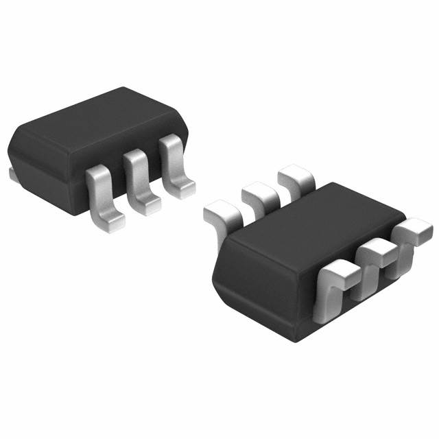
SC-70 (6 leads)
SOT-363 Single
D
6
• TrenchFET® power MOSFET
S
4
D
5
• Typical ESD performance 1500 V
• 100 % Rg tested
• Material categorization:
for definitions of compliance please
see www.vishay.com/doc?99912
1
D
Top View
2
D
3
G
APPLICATIONS
• Load switch for portable devices
- Cellular phone
- DSC
- Portable game console
- MP3
- GPS
Marking code: BQ
PRODUCT SUMMARY
VDS (V)
G
R
-20
RDS(on) max. () at VGS = -4.5 V
0.041
RDS(on) max. () at VGS = -2.5 V
0.054
RDS(on) max. () at VGS = -1.8 V
0.100
Qg typ. (nC)
12.5
ID (A) a
Configuration
S
D
P-Channel MOSFET
-4
Single
ORDERING INFORMATION
Package
Lead (Pb)-free and halogen-free
SC-70
Si1441EDH-T1-GE3
ABSOLUTE MAXIMUM RATINGS (TA = 25 °C, unless otherwise noted)
PARAMETER
Drain-source voltage
Gate-source voltage
Continuous drain current (TJ = 150 °C)
TC = 25 °C
TC = 70 °C
TA = 25 °C
TA = 70 °C
Pulsed drain current (t = 300 μs)
Continuous source-drain diode current
Maximum power dissipation
SYMBOL
LIMIT
VDS
VGS
-20
± 10
-4 a
-4
-4 a, b, c
-4 a, b, c
-25
-2.3
-1.3 b, c
2.8
1.8
1.6 b, c
1 b, c
-55 to +150
260
ID
IDM
TC = 25 °C
TA = 25 °C
TC = 25 °C
TC = 70 °C
TA = 25 °C
TA = 70 °C
Operating junction and storage temperature range
Soldering recommendations (peak temperature)
IS
PD
TJ, Tstg
UNIT
V
A
W
°C
THERMAL RESISTANCE RATINGS
PARAMETER
Maximum junction-to-ambient b, d
Maximum junction-to-foot (drain)
t5s
Steady state
SYMBOL
TYPICAL
MAXIMUM
UNIT
RthJA
RthJF
60
34
80
45
°C/W
Notes
a. Package limited
b. Surface mounted on 1" x 1" FR4 board
c. t = 5 s
d. Maximum under steady state conditions is 125 °C/W
S10-1827-Rev. A, 09-Aug-10
Document Number: 66823
1
For technical questions, contact: pmostechsupport@vishay.com
THIS DOCUMENT IS SUBJECT TO CHANGE WITHOUT NOTICE. THE PRODUCTS DESCRIBED HEREIN AND THIS DOCUMENT
ARE SUBJECT TO SPECIFIC DISCLAIMERS, SET FORTH AT www.vishay.com/doc?91000
�Si1441EDH
www.vishay.com
Vishay Siliconix
SPECIFICATIONS (TJ = 25 °C, unless otherwise noted)
PARAMETER
SYMBOL
TEST CONDITIONS
MIN.
TYP.
MAX.
UNIT
VDS
VGS = 0 V, ID = -250 μA
-20
-
-
-
V
-11
-
-
2.6
-
VDS = VGS, ID = -250 μA
-0.4
-
-1
VDS = 0 V, VGS = ± 10 V
-
-
±8
Static
Drain-source breakdown voltage
VDS/TJ
VDS temperature coefficient
VGS(th) temperature coefficient
VGS(th)/TJ
Gate-source threshold voltage
VGS(th)
Gate-source leakage
Zero gate voltage drain current
On-state drain
current a
Drain-source on-state resistance a
Forward transconductance a
IGSS
IDSS
ID(on)
RDS(on)
gfs
ID = -250 μA
VDS = 0 V, VGS = ± 4.5 V
-
-
±1
VDS = -20 V, VGS = 0 V
-
-
-1
VDS = -20 V, VGS = 0 V, TJ = 55 °C
-
-
-10
VDS -5 V, VGS = -10 V
-15
-
-
VGS = -4.5 V, ID = -5 A
-
0.034
0.041
VGS = -2.5 V, ID = -4.4 A
-
0.045
0.054
VGS = -1.8 V, ID = -1 A
-
0.067
0.100
VDS = -10 V, ID = -5 A
-
16
-
VDS = -10 V, VGS = -8 V, ID = -5 A
-
22
33
-
12.5
19
VDS = -10 V, VGS = -4.5 V, ID = -5 A
-
1.8
-
-
3.3
-
f = 1 MHz
80
430
860
-
150
225
mV/°C
V
μA
A
S
Dynamic b
Total gate charge
Qg
Gate-source charge
Qgs
Gate-drain charge
Qgd
Gate resistance
Rg
Turn-on delay time
Rise time
Turn-off delay time
Fall time
Turn-on delay time
Rise time
Turn-off delay time
Fall time
td(on)
tr
VDD = -10 V, RL = 1.4
ID -4 A, VGEN = -4.5 V, Rg = 1
-
300
450
-
1620
2430
tf
-
560
840
td(on)
-
50
100
td(off)
tr
td(off)
VDD = -10 V, RL = 1.4
ID -4 A, VGEN = -10 V, Rg = 1
tf
-
90
180
-
2500
3750
-
600
900
nC
ns
Drain-Source Body Diode Characteristics
Continuous source-drain diode current
IS
Pulse diode forward current
ISM
Body diode voltage
VSD
Body diode reverse recovery time
trr
Body diode reverse recovery charge
Qrr
Reverse recovery fall time
ta
Reverse recovery rise time
tb
TC = 25 °C
IS = -4 A, VGS = 0 V
IF = -4 A, di/dt = 100 A/μs,
TJ = 25 °C
-
-
-2.3
-
-
-25
-
-0.85
-1.2
V
-
18
36
ns
-
8
16
nC
-
18
-
-
10
-
A
ns
Notes
a. Pulse test; pulse width 300 μs, duty cycle 2 %
b. Guaranteed by design, not subject to production testing
Stresses beyond those listed under “Absolute Maximum Ratings” may cause permanent damage to the device. These are stress ratings only, and functional operation
of the device at these or any other conditions beyond those indicated in the operational sections of the specifications is not implied. Exposure to absolute maximum
rating conditions for extended periods may affect device reliability.
S10-1827-Rev. A, 09-Aug-10
Document Number: 66823
2
For technical questions, contact: pmostechsupport@vishay.com
THIS DOCUMENT IS SUBJECT TO CHANGE WITHOUT NOTICE. THE PRODUCTS DESCRIBED HEREIN AND THIS DOCUMENT
ARE SUBJECT TO SPECIFIC DISCLAIMERS, SET FORTH AT www.vishay.com/doc?91000
�Si1441EDH
www.vishay.com
Vishay Siliconix
TYPICAL CHARACTERISTICS (25 °C, unless otherwise noted)
0.1
10-4
10-5
IGSS - Gate Current (A)
IGSS - Gate Current (mA)
0.08
0.06
0.04
0.02
0
TJ = 150 °C
10-6
10-7
TJ = 25 °C
10-8
10-9
0
3
6
9
12
10-10
15
0
3
6
9
12
VGS - Gate-Source Voltage (V)
VGS - Gate-Source Voltage (V)
Gate Current vs. Gate-Source Voltage
Gate Current vs. Gate-Source Voltage
25
15
5
V GS = 5 V thru 3 V
V GS = 2.5 V
4
ID - Drain Current (A)
ID - Drain Current (A)
20
15
V GS = 2 V
10
V GS = 1.5 V
5
3
T C = 25 °C
2
T C = 125 °C
1
T C = - 55 °C
0
0
0
0.5
1.0
1.5
2.0
2.5
0
0.5
1.0
1.5
2.0
VDS - Drain-to-Source Voltage (V)
VGS - Gate-to-Source Voltage (V)
Output Characteristics
Transfer Characteristics
0.10
8
V GS = 1.8 V
VGS - Gate-to-Source Voltage (V)
RDS(on) - On-Resistance (Ω)
ID = 5 A
0.08
V GS = 2.5 V
0.06
V GS = 4.5 V
0.04
0.02
0
6
V DS = 5 V
V DS = 10 V
4
V DS = 16 V
2
0
0
5
10
15
20
25
0
5
10
15
ID - Drain Current (A)
Qg - Total Gate Charge (nC)
On-Resistance vs. Drain Current
Gate Charge
S10-1827-Rev. A, 09-Aug-10
20
25
Document Number: 66823
3
For technical questions, contact: pmostechsupport@vishay.com
THIS DOCUMENT IS SUBJECT TO CHANGE WITHOUT NOTICE. THE PRODUCTS DESCRIBED HEREIN AND THIS DOCUMENT
ARE SUBJECT TO SPECIFIC DISCLAIMERS, SET FORTH AT www.vishay.com/doc?91000
�Si1441EDH
www.vishay.com
Vishay Siliconix
TYPICAL CHARACTERISTICS (25 °C, unless otherwise noted)
1.5
100
IS - Source Current (A)
1.3
(Normalized)
RDS(on) - On-Resistance
V GS = - 4.5 V; ID = - 5 A
V GS = - 2.5 V;
ID = - 4.4 A
1.1
0.9
0.7
- 50
T J = 150 °C
10
T J = 25 °C
1
0.1
- 25
0
25
50
75
100
125
150
0
0.5
1.0
VSD - Source-to-Drain Voltage (V)
TJ - Junction Temperature (°C)
Source-Drain Diode Forward Voltage
On-Resistance vs. Junction Temperature
0.90
0.10
0.75
0.08
ID = - 250 μA
VGS(th) (V)
RDS(on) - On-Resistance (Ω)
ID = - 5 A
0.06
T J = 125 °C
0.04
0.45
T J = 25 °C
0.30
- 50
0.02
1
2
3
4
0.60
5
- 25
0
25
50
75
100
125
150
VGS - Gate-to-Source Voltage (V)
TJ - Temperature (°C)
On-Resistance vs. Gate-to-Source Voltage
Single Pulse Power, Junction-to-Ambient
100
30
Limited by RDS(on) *
10
ID - Drain Current (A)
Power (W)
24
18
12
100 μs
1 ms
1
10 ms
100 ms
1 s, 10 s
DC
0.1
6
0
0.001
TA = 25 °C
Single Pulse
0.01
0.1
Time (s)
Threshold Voltage
S10-1827-Rev. A, 09-Aug-10
1
10
0.01
0.1
BVDSS Limited
1
10
100
VDS - Drain-to-Source Voltage (V)
* VGS > minimum VGS at which RDS(on) is specified
Safe Operating Area, Junction-to-Ambient
Document Number: 66823
4
For technical questions, contact: pmostechsupport@vishay.com
THIS DOCUMENT IS SUBJECT TO CHANGE WITHOUT NOTICE. THE PRODUCTS DESCRIBED HEREIN AND THIS DOCUMENT
ARE SUBJECT TO SPECIFIC DISCLAIMERS, SET FORTH AT www.vishay.com/doc?91000
�Si1441EDH
www.vishay.com
Vishay Siliconix
TYPICAL CHARACTERISTICS (25 °C, unless otherwise noted)
8
ID - Drain Current (A)
6
Package Limited
4
2
0
0
25
50
75
100
125
150
TC - Case Temperature (°C)
4
1.2
3
0.9
Power (W)
Power (W)
Current Derating a
2
0.6
0.3
1
0.0
0
0
25
50
75
100
125
150
0
25
50
75
100
125
TC - Case Temperature (°C)
TA - Ambient Temperature (°C)
Power Derating, Junction-to-Foot
Power Derating, Junction-to-Ambient
150
Note
a. The power dissipation PD is based on TJ max. = 150 °C, using junction-to-case thermal resistance, and is more useful in settling the upper
dissipation limit for cases where additional heatsinking is used. It is used to determine the current rating, when this rating falls below the
package limit
S10-1827-Rev. A, 09-Aug-10
Document Number: 66823
5
For technical questions, contact: pmostechsupport@vishay.com
THIS DOCUMENT IS SUBJECT TO CHANGE WITHOUT NOTICE. THE PRODUCTS DESCRIBED HEREIN AND THIS DOCUMENT
ARE SUBJECT TO SPECIFIC DISCLAIMERS, SET FORTH AT www.vishay.com/doc?91000
�Si1441EDH
www.vishay.com
Vishay Siliconix
TYPICAL CHARACTERISTICS (25 °C, unless otherwise noted)
1
Normalized Effective Transient
Thermal Impedance
Duty Cycle = 0.5
0.2
Notes:
0.1
0.1
PDM
0.05
t1
t2
0.02
t1
t2
2. Per Unit Base = RthJA = 125 °C/W
1. Duty Cycle, D =
3. TJM - TA = PDMZthJA (t)
Single Pulse
0.01
10-4
10
4. Surface Mounted
-3
-2
10
-1
10
1
10
100
1000
Square Wave Pulse Duration (s)
Normalized Thermal Transient Impedance, Junction-to-Ambient
1
Normalized Effective Transient
Thermal Impedance
Duty Cycle = 0.5
0.2
0.1
0.1
0.05
0.02
Single Pulse
0.01
10-4
10-3
10-2
10-1
1
10
Square Wave Pulse Duration (s)
Normalized Thermal Transient Impedance, Junction-to-Foot
Vishay Siliconix maintains worldwide manufacturing capability. Products may be manufactured at one of several qualified locations. Reliability data for silicon
technology and package reliability represent a composite of all qualified locations. For related documents such as package / tape drawings, part marking, and
reliability data, see www.vishay.com/ppg?66823.
S10-1827-Rev. A, 09-Aug-10
Document Number: 66823
6
For technical questions, contact: pmostechsupport@vishay.com
THIS DOCUMENT IS SUBJECT TO CHANGE WITHOUT NOTICE. THE PRODUCTS DESCRIBED HEREIN AND THIS DOCUMENT
ARE SUBJECT TO SPECIFIC DISCLAIMERS, SET FORTH AT www.vishay.com/doc?91000
�Package Information
Vishay Siliconix
SCĆ70:
6ĆLEADS
MILLIMETERS
6
5
Dim
A
A1
A2
b
c
D
E
E1
e
e1
L
4
E1 E
1
2
3
-B-
e
b
e1
D
-Ac
A2 A
L
A1
Document Number: 71154
06-Jul-01
INCHES
Min
Nom
Max
Min
Nom
Max
0.90
–
1.10
0.035
–
0.043
–
–
0.10
–
–
0.004
0.80
–
1.00
0.031
–
0.039
0.15
–
0.30
0.006
–
0.012
0.10
–
0.25
0.004
–
0.010
1.80
2.00
2.20
0.071
0.079
0.087
1.80
2.10
2.40
0.071
0.083
0.094
1.15
1.25
1.35
0.045
0.049
0.053
0.65BSC
0.026BSC
1.20
1.30
1.40
0.047
0.051
0.055
0.10
0.20
0.30
0.004
0.008
0.012
7_Nom
7_Nom
ECN: S-03946—Rev. B, 09-Jul-01
DWG: 5550
www.vishay.com
1
�AN815
Vishay Siliconix
Single-Channel LITTLE FOOTR SC-70 6-Pin MOSFET
Copper Leadframe Version
Recommended Pad Pattern and Thermal Performance
INTRODUCTION
EVALUATION BOARDS � SINGLE SC70-6
The new single 6-pin SC-70 package with a copper leadframe
enables improved on-resistance values and enhanced
thermal performance as compared to the existing 3-pin and
6-pin packages with Alloy 42 leadframes. These devices are
intended for small to medium load applications where a
miniaturized package is required. Devices in this package
come in a range of on-resistance values, in n-channel and
p-channel versions. This technical note discusses pin-outs,
package outlines, pad patterns, evaluation board layout, and
thermal performance for the single-channel version.
The evaluation board (EVB) measures 0.6 inches by
0.5 inches. The copper pad traces are the same as in Figure 2.
The board allows examination from the outer pins to 6-pin DIP
connections, permitting test sockets to be used in evaluation
testing. See Figure 3.
52 (mil)
BASIC PAD PATTERNS
See Application Note 826, Recommended Minimum Pad
Patterns With Outline Drawing Access for Vishay Siliconix
MOSFETs, (http://www.vishay.com/doc?72286) for the basic
pad layout and dimensions. These pad patterns are sufficient
for the low to medium power applications for which this
package is intended. Increasing the drain pad pattern yields a
reduction in thermal resistance and is a preferred footprint.
The availability of four drain leads rather than the traditional
single drain lead allows a better thermal path from the package
to the PCB and external environment.
96 (mil)
6
5
4
1
2
3
71 (mil)
26 (mil)
13 (mil)
0, 0 (mil)
18 (mil)
26 (mil)
PIN-OUT
16 (mil)
Figure 1 shows the pin-out description and Pin 1
identification.The pin-out of this device allows the use of four
pins as drain leads, which helps to reduce on-resistance and
junction-to-ambient thermal resistance.
SOT-363
SC-70 (6-LEADS)
D
1
6
D
D
2
5
D
G
3
4
S
FIGURE 2.
SC-70 (6 leads) Single
The thermal performance of the single 6-pin SC-70 has been
measured on the EVB, comparing both the copper and
Alloy 42 leadframes. This test was first conducted on the
traditional Alloy 42 leadframe and was then repeated using the
1-inch2 PCB with dual-side copper coating.
Top View
FIGURE 1.
For package dimensions see outline drawing SC-70 (6-Leads)
(http://www.vishay.com/doc?71154)
Document Number: 71334
12-Dec-03
www.vishay.com
1
�AN815
Vishay Siliconix
Front of Board SC70-6
Back of Board SC70-6
vishay.com
FIGURE 3.
THERMAL PERFORMANCE
Junction-to-Foot Thermal Resistance
(Package Performance)
COOPER LEADFRAME
Room Ambient 25 _C
The junction to foot thermal resistance is a useful method of
comparing different packages thermal performance.
A helpful way of presenting the thermal performance of the
6-Pin SC-70 copper leadframe device is to compare it to the
traditional Alloy 42 version.
Thermal performance for the 6-pin SC-70 measured as
junction-to-foot thermal resistance, where the “foot” is the
drain lead of the device at the bottom where it meets the PCB.
The junction-to-foot thermal resistance is typically 40_C/W in
the copper leadframe and 163_C/W in the Alloy 42 leadframe
— a four-fold improvement. This improved performance is
obtained by the enhanced thermal conductivity of copper over
Alloy 42.
The typical RqJA for the single 6-pin SC-70 with copper
leadframe is 103_C/W steady-state, compared with 212_C/W
for the Alloy 42 version. The figures are based on the 1-inch2
FR4 test board. The following example shows how the thermal
resistance impacts power dissipation for the two different
leadframes at varying ambient temperatures.
ALLOY 42 LEADFRAME
PD +
Rq JA
Elevated Ambient 60 _C
PD +
T J(max) * T A
Rq JA
o
o
P D + 150 Co* 25 C
212 CńW
o
o
P D + 150 Co* 25 C
212 CńW
P D + 590 mW
P D + 425 mW
www.vishay.com
2
T J(max) * T A
T J(max) * T A
Rq JA
PD +
T J(max) * T A
Rq JA
o
o
P D + 150 Co* 25 C
124 CńW
o
o
P D + 150 Co* 60 C
124 CńW
P D + 1.01 W
P D + 726 mW
As can be seen from the calculations above, the compact 6-pin
SC-70 copper leadframe LITTLE FOOT power MOSFET can
handle up to 1 W under the stated conditions.
Testing
To further aid comparison of copper and Alloy 42 leadframes,
Figure 5 illustrates single-channel 6-pin SC-70 thermal
performance on two different board sizes and two different pad
patterns. The measured steady-state values of RqJA for the
two leadframes are as follows:
LITTLE FOOT 6-PIN SC-70
Power Dissipation
Room Ambient 25 _C
PD +
Elevated Ambient 60 _C
1) Minimum recommended pad pattern on
the EVB board V (see Figure 3.
1-inch2
2) Industry standard
PCB with
maximum copper both sides.
Alloy 42
Copper
329.7_C/W
208.5_C/W
211.8_C/W
103.5_C/W
The results indicate that designers can reduce thermal
resistance (RqJA) by 36% simply by using the copper
leadframe device rather than the Alloy 42 version. In this
example, a 121_C/W reduction was achieved without an
increase in board area. If increasing in board size is feasible,
a further 105_C/W reduction could be obtained by utilizing a
1-inch2 square PCB area.
The copper leadframe versions have the following suffix:
Single:
Si14xxEDH
Dual:
Si19xxEDH
Complementary: Si15xxEDH
Document Number: 71334
12-Dec-03
�AN815
400
250
320
200
240
Thermal Resistance (C/W)
Thermal Resistance (C/W)
Vishay Siliconix
Alloy
42
160
Copper
80
150
Alloy
42
100
50
Copper
0
0
10-5
10-4
10-3
10-2
10-1
1
10
100
1000
10-5
Leadframe Comparison on EVB
Document Number: 71334
12-Dec-03
10-3
10-2
10-1
1
10
100
1000
Time (Secs)
Time (Secs)
FIGURE 4.
10-4
FIGURE 5.
Leadframe Comparison on Alloy 42 1-inch2 PCB
www.vishay.com
3
�Application Note 826
Vishay Siliconix
RECOMMENDED MINIMUM PADS FOR SC-70: 6-Lead
0.067
0.026
(0.648)
0.045
(1.143)
0.096
(2.438)
(1.702)
0.016
0.026
0.010
(0.406)
(0.648)
(0.241)
Recommended Minimum Pads
Dimensions in Inches/(mm)
Return to Index
APPLICATION NOTE
Return to Index
www.vishay.com
18
Document Number: 72602
Revision: 21-Jan-08
�Legal Disclaimer Notice
www.vishay.com
Vishay
Disclaimer
ALL PRODUCT, PRODUCT SPECIFICATIONS AND DATA ARE SUBJECT TO CHANGE WITHOUT NOTICE TO IMPROVE
RELIABILITY, FUNCTION OR DESIGN OR OTHERWISE.
Vishay Intertechnology, Inc., its affiliates, agents, and employees, and all persons acting on its or their behalf (collectively,
“Vishay”), disclaim any and all liability for any errors, inaccuracies or incompleteness contained in any datasheet or in any other
disclosure relating to any product.
Vishay makes no warranty, representation or guarantee regarding the suitability of the products for any particular purpose or
the continuing production of any product. To the maximum extent permitted by applicable law, Vishay disclaims (i) any and all
liability arising out of the application or use of any product, (ii) any and all liability, including without limitation special,
consequential or incidental damages, and (iii) any and all implied warranties, including warranties of fitness for particular
purpose, non-infringement and merchantability.
Statements regarding the suitability of products for certain types of applications are based on Vishay's knowledge of typical
requirements that are often placed on Vishay products in generic applications. Such statements are not binding statements
about the suitability of products for a particular application. It is the customer's responsibility to validate that a particular product
with the properties described in the product specification is suitable for use in a particular application. Parameters provided in
datasheets and / or specifications may vary in different applications and performance may vary over time. All operating
parameters, including typical parameters, must be validated for each customer application by the customer's technical experts.
Product specifications do not expand or otherwise modify Vishay's terms and conditions of purchase, including but not limited
to the warranty expressed therein.
Hyperlinks included in this datasheet may direct users to third-party websites. These links are provided as a convenience and
for informational purposes only. Inclusion of these hyperlinks does not constitute an endorsement or an approval by Vishay of
any of the products, services or opinions of the corporation, organization or individual associated with the third-party website.
Vishay disclaims any and all liability and bears no responsibility for the accuracy, legality or content of the third-party website
or for that of subsequent links.
Except as expressly indicated in writing, Vishay products are not designed for use in medical, life-saving, or life-sustaining
applications or for any other application in which the failure of the Vishay product could result in personal injury or death.
Customers using or selling Vishay products not expressly indicated for use in such applications do so at their own risk. Please
contact authorized Vishay personnel to obtain written terms and conditions regarding products designed for such applications.
No license, express or implied, by estoppel or otherwise, to any intellectual property rights is granted by this document or by
any conduct of Vishay. Product names and markings noted herein may be trademarks of their respective owners.
© 2021 VISHAY INTERTECHNOLOGY, INC. ALL RIGHTS RESERVED
Revision: 09-Jul-2021
1
Document Number: 91000
�


 工商网监
湘ICP备2023018690号
工商网监
湘ICP备2023018690号
