VEMT3700
Vishay Semiconductors
Silicon NPN Phototransistor
FEATURES
•
•
•
•
•
•
•
•
•
•
•
•
•
94 8553
DESCRIPTION
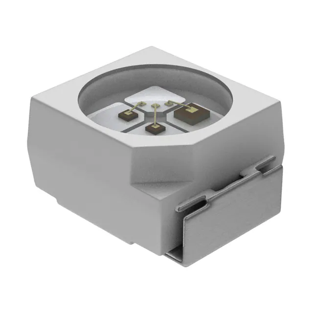
VEMT3700 is a high speed silicon NPN epitaxial planar
phototransistor in a miniature PLCC-2 package for surface
mounting on printed boards. The device is sensitive to
visible and near infrared radiation.
Package type: surface mount
Package form: PLCC-2
Dimensions (L x W x H in mm): 3.5 x 2.8 x 1.75
High photo sensitivity
High radiant sensitivity
Suitable for visible and near infrared radiation
Fast response times
Angle of half sensitivity: ϕ = ± 60°
Package notch indicates collector
Package matched with IR emitter series VSML3710
Floor life: 168 h, MSL 3, acc. J-STD-020
Lead (Pb)-free reflow soldering
Compliant to RoHS directive 2002/95/EC and in
accordance to WEEE 2002/96/EC
APPLICATIONS
•
•
•
•
•
•
Photo interrupters
Miniature switches
Counters
Encoders
Position sensors
Ligth sensors
PRODUCT SUMMARY
COMPONENT
VEMT3700
Ica (mA)
ϕ (deg)
λ0.1 (nm)
0.5
± 60
450 to 1080
Note
• Test conditions see table “Basic Characteristics”
ORDERING INFORMATION
ORDERING CODE
PACKAGING
REMARKS
PACKAGE FORM
VEMT3700-GS08
VEMT3700-GS18
Tape and reel
Tape and reel
MOQ: 7500 pcs, 1500 pcs/reel
MOQ: 8000 pcs, 8000 pcs/reel
PLCC-2
PLCC-2
Note
• MOQ: minimum order quantity
ABSOLUTE MAXIMUM RATINGS (Tamb = 25 °C, unless otherwise specified)
PARAMETER
TEST CONDITION
Collector emitter voltage
Emitter collector voltage
Collector current
Collector peak current
Power dissipation
Junction temperature
Operating temperature range
Storage temperature range
Soldering temperature
Thermal resistance junction/ambient
tp/T ≤ 0.1, tp ≤ 10 μs
Acc. reflow solder profile fig. 10
Soldered on PCB with pad dimensions: 4 mm x 4 mm
SYMBOL
VALUE
UNIT
VCEO
VECO
IC
ICM
PV
Tj
Tamb
Tstg
Tsd
RthJA
70
5
50
100
100
100
- 40 to + 100
- 40 to + 100
260
400
V
V
mA
mA
mW
°C
°C
°C
°C
K/W
** Please see document “Vishay Material Category Policy”: www.vishay.com/doc?99902
Document Number: 81478
Rev. 1.6, 14-Jul-10
For technical questions, contact: detectortechsupport@vishay.com
www.vishay.com
1
�VEMT3700
Silicon NPN Phototransistor
Vishay Semiconductors
PV - Power Dissipation Limit (mW)
125
R thJA = 400 K/W
100
75
50
25
0
10 20 30 40 50 60 70 80 90 100
0
Tamb - Ambient Temperature (°C)
20376
Fig. 1 - Power Dissipation Limit vs. Ambient Temperature
BASIC CHARACTERISTICS (Tamb = 25 °C, unless otherwise specified)
PARAMETER
TEST CONDITION
SYMBOL
MIN.
IC = 1 mA
V(BR)CEO
70
TYP.
MAX.
UNIT
VCE = 20 V, E = 0
ICEO
1
200
nA
VCE = 5 V, f = 1 MHz, E = 0
CCEO
3
pF
Ee = 1 mW/cm2, λ = 950 nm,
VCE = 5 V
Ica
0.5
mA
Collector emitter breakdown voltage
Collector emitter dark current
Collector emitter capacitance
Collector ligth current
V
0.25
Angle of half sensitivity
ϕ
± 60
deg
Wavelength of peak sensitivity
λp
850
nm
λ0.1
450 to 1080
nm
Ee = 1 mW/cm2, λ = 950 nm,
IC = 0.1 mA
VCEsat
0.15
VS = 5 V, IC = 1 mA, λ = 950 nm,
RL = 1 kΩ
tr/tf
6
μs
VS = 5 V, IC = 1 mA, λ = 950 nm,
RL = 100 Ω
tr/tf
2
μs
VS = 5 V, IC = 2 mA, RL = 100 Ω
fc
180
kHz
Range of spectral bandwidth
Collector emitter saturation voltage
Rise time, fall time
Cut-off frequency
0.3
V
BASIC CHARACTERISTICS (Tamb = 25 °C, unless otherwise specified)
2.0
Ica rel - Relative Collector Current
ICEO - Collector Dark Current (nA)
104
103
VCE = 20 V
102
101
10
1.8
VCE = 5 V
Ee = 1 mW/cm2
λ = 950 nm
1.6
1.4
1.2
1.0
0.8
0.6
20
94 8304
40
60
80
Tamb - Ambient Temperature (°C)
Fig. 2 - Collector Dark Current vs. Ambient Temperature
www.vishay.com
2
0
100
94 8239
20
40
60
80
100
Tamb - Ambient Temperature (°C)
Fig. 3 - Relative Collector Current vs. Ambient Temperature
For technical questions, contact: detectortechsupport@vishay.com
Document Number: 81478
Rev. 1.6, 14-Jul-10
�VEMT3700
Silicon NPN Phototransistor
8
ton/toff - Turn-on/Turn-off Time (µs)
Ica - Collector Light Current (mA)
10
Vishay Semiconductors
1
0.1
VCE = 5 V
λ = 950 nm
0.01
0.001
0.01
4
toff
2
ton
0
0.1
1
10
Ee - Irradiance (mW/cm²)
94 8316
VCE = 5 V
RL = 100 Ω
λ = 950 nm
6
0
2
6
8
10
12
14
IC - Collector Current (mA)
94 8293
Fig. 4 - Collector Light Current vs. Irradiance
4
Fig. 7 - Turn-on/Turn-off Time vs. Collector Current
S (λ)rel - Relative Spectral Sensitivity
Ica - Collector Light Current (mA)
10
λ = 950 nm
1
Ee = 1 mW/cm2
0.5 mW/cm2
0.2 mW/cm2
0.1
0.1
94 8317
1
10
0.8
0.6
0.4
0.2
0
100
VCE - Collector Emitter Voltage (V)
400
600
800
1000
λ - Wavelength (nm)
94 8348
Fig. 5 - Collector Light Current vs. Collector Emitter Voltage
Fig. 8 - Relative Spectral Sensitivity vs. Wavelength
0°
10
10°
20°
30°
8
6
4
2
40°
1.0
0.9
50°
0.8
60°
70°
0.7
ϕ - Angular Displacement
f = 1 MHz
Srel - Relative Sensitivity
CCEO - Collector Emitter Capacitance (pF)
1.0
80°
0
0.1
94 8294
1
10
100
VCE - Collector Emitter Voltage (V)
Fig. 6 - Collector Emitter Capacitance vs. Collector Emitter Voltage
Document Number: 81478
Rev. 1.6, 14-Jul-10
0.6
0.4
0.2
0
94 8318
Fig. 9 - Relative Radiant Sensitivity vs. Angular Displacement
For technical questions, contact: detectortechsupport@vishay.com
www.vishay.com
3
�VEMT3700
Silicon NPN Phototransistor
Vishay Semiconductors
PACKAGE DIMENSIONS in millimeters
Mounting Pad Layout
1.2
4
2.6 (2.8)
area covered with
solder resist
4
1.6 (1.9)
20873
SOLDER PROFILE
DRYPACK
300
255 °C
240 °C
217 °C
250
Temperature (°C)
max. 260 °C
245 °C
FLOOR LIFE
200
max. 30 s
150
max. 100 s
max. 120 s
100
max. ramp up 3 °C/s max. ramp down 6 °C/s
50
0
50
100
150
200
250
300
Time (s)
Fig. 10 - Lead (Pb)-free Reflow Solder Profile acc. J-STD-020
www.vishay.com
4
Floor life (time between soldering and removing from MBB)
must not exceed the time indicated on MBB label:
Floor life: 168 h
Conditions: Tamb < 30 °C, RH < 60 %
Moisture sensitivity level 3, acc. to J-STD-020.
DRYING
0
19841
Devices are packed in moisture barrier bags (MBB) to
prevent the products from moisture absorption during
transportation and storage. Each bag contains a desiccant.
In case of moisture absorption devices should be baked
before soldering. Conditions see J-STD-020 or label.
Devices taped on reel dry using recommended conditions
192 h at 40 °C (+ 5 °C), RH < 5 %.
For technical questions, contact: detectortechsupport@vishay.com
Document Number: 81478
Rev. 1.6, 14-Jul-10
�VEMT3700
Silicon NPN Phototransistor
Vishay Semiconductors
TAPE AND REEL
PLCC-2 components are packed in antistatic blister tape
(DIN IEC (CO) 564) for automatic component insertion.
Cavities of blister tape are covered with adhesive tape.
component is followed by a carrier tape trailer with a least
75 empty compartments and sealed with cover tape.
10.0
9.0
120°
Adhesive tape
4.5
3.5
2.5
1.5
Blister tape
Component cavity
Identification
Label:
Vishay
type
group
tape code
production
code
quantity
94 8670
Fig. 11 - Blister Tape
13.00
12.75
63.5
60.5
14.4 max.
180
178
94 8665
Fig. 14 - Dimensions of Reel-GS08
3.5
3.1
2.2
2.0
3.6
3.4
4.0
3.6
4.5
3.5
8.3
7.7
2.5
1.5
1.85
1.65
1.6
1.4
4.1
3.9
4.1
3.9
10.4
8.4
120°
5.75
5.25
0.25
Identification
Label:
Vishay
type
group
tape code
production
code
quantity
2.05
1.95
94 8668
Fig. 12 - Tape Dimensions in mm for PLCC-2
MISSING DEVICES
A maximum of 0.5 % of the total number of components per
reel may be missing, exclusively missing components at the
beginning and at the end of the reel. A maximum of three
consecutive components may be missing, provided this gap
is followed by six consecutive components.
De-reeling direction
94 8158
13.00
12.75
62.5
60.0
321
329
14.4 max.
18857
Fig. 15 - Dimensions of Reel-GS18
COVER TAPE REMOVAL FORCE
The removal force lies between 0.1 N and 1.0 N at a removal
speed of 5 mm/s. In order to prevent components from
popping out of the blisters, the cover tape must be pulled off
at an angle of 180° with regard to the feed direction.
> 160 mm
Tape leader
40 empty
compartments
min. 75 empty
compartments
Carrier leader
Carrier trailer
Fig. 13 - Beginning and End of Reel
The tape leader is at least 160 mm and is followed by a
carrier tape leader with at least 40 empty compartments.
The tape leader may include the carrier tape as long as the
cover tape is not connected to the carrier tape. The least
Document Number: 81478
Rev. 1.6, 14-Jul-10
For technical questions, contact: detectortechsupport@vishay.com
www.vishay.com
5
�Legal Disclaimer Notice
www.vishay.com
Vishay
Disclaimer
ALL PRODUCT, PRODUCT SPECIFICATIONS AND DATA ARE SUBJECT TO CHANGE WITHOUT NOTICE TO IMPROVE
RELIABILITY, FUNCTION OR DESIGN OR OTHERWISE.
Vishay Intertechnology, Inc., its affiliates, agents, and employees, and all persons acting on its or their behalf (collectively,
“Vishay”), disclaim any and all liability for any errors, inaccuracies or incompleteness contained in any datasheet or in any other
disclosure relating to any product.
Vishay makes no warranty, representation or guarantee regarding the suitability of the products for any particular purpose or
the continuing production of any product. To the maximum extent permitted by applicable law, Vishay disclaims (i) any and all
liability arising out of the application or use of any product, (ii) any and all liability, including without limitation special,
consequential or incidental damages, and (iii) any and all implied warranties, including warranties of fitness for particular
purpose, non-infringement and merchantability.
Statements regarding the suitability of products for certain types of applications are based on Vishay's knowledge of typical
requirements that are often placed on Vishay products in generic applications. Such statements are not binding statements
about the suitability of products for a particular application. It is the customer's responsibility to validate that a particular product
with the properties described in the product specification is suitable for use in a particular application. Parameters provided in
datasheets and / or specifications may vary in different applications and performance may vary over time. All operating
parameters, including typical parameters, must be validated for each customer application by the customer's technical experts.
Product specifications do not expand or otherwise modify Vishay's terms and conditions of purchase, including but not limited
to the warranty expressed therein.
Hyperlinks included in this datasheet may direct users to third-party websites. These links are provided as a convenience and
for informational purposes only. Inclusion of these hyperlinks does not constitute an endorsement or an approval by Vishay of
any of the products, services or opinions of the corporation, organization or individual associated with the third-party website.
Vishay disclaims any and all liability and bears no responsibility for the accuracy, legality or content of the third-party website
or for that of subsequent links.
Except as expressly indicated in writing, Vishay products are not designed for use in medical, life-saving, or life-sustaining
applications or for any other application in which the failure of the Vishay product could result in personal injury or death.
Customers using or selling Vishay products not expressly indicated for use in such applications do so at their own risk. Please
contact authorized Vishay personnel to obtain written terms and conditions regarding products designed for such applications.
No license, express or implied, by estoppel or otherwise, to any intellectual property rights is granted by this document or by
any conduct of Vishay. Product names and markings noted herein may be trademarks of their respective owners.
© 2022 VISHAY INTERTECHNOLOGY, INC. ALL RIGHTS RESERVED
Revision: 01-Jan-2022
1
Document Number: 91000
�


 工商网监
湘ICP备2023018690号
工商网监
湘ICP备2023018690号
