TB9061AFNG
TOSHIBA Bi-CMOS Integrated Circuit Silicon Monolithic
TB9061AFNG
3-Phase Sensorless Brushless Motor Pre-driver
The TB9061AFNG is an automotive pre-driver IC that incorporates
a sensorless controller for driving a 3-phase full-wave brushless DC
motor.
Feature
・3-phase full-wave sensorless drive
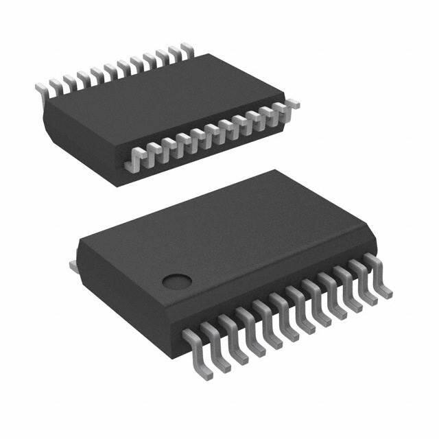
SSOP24-P-300-0.65A
・PWM chopper drive
・Outputs for external P-ch/N-ch MOSFETs drive ( 3-phase 6 outputs)
Weight: 0.14 g (typ.)
(Output PWM Dynamic range expansion)
・Suited for both PWM input and DC input control
・Rotating Direction: CW/CCW
・PWM control on lower driver outputs
・Built-in 8-bit AD converter
・Built-in 3-ch comparators to detect induced voltage (Independent 3-phase inputs)
・Built-in overcurrent detector: Detect two values (Current limiter/Overcurrent detection)
・Built-in loss-of-synchronism detection and automatic restart control (Improved Start up)
・5.12-MHz oscillator for reference clock
・Built-in 5-V constant voltage circuit
・Operating temperature range: -40 to125 °C
・Mini flat package: SSOP-24pin(pin pitch:0.65 mm)
・TB9061FNG Pin-compatible
・The product(s) is/are compatible with RoHS regulations (EU directive 2011 / 65 / EU) as indicated, if any, on the
packaging label ("[[G]]/RoHS COMPATIBLE", "[[G]]/RoHS [[Chemical symbol(s) of controlled substance(s)]]", "RoHS
COMPATIBLE" or "RoHS COMPATIBLE, [[Chemical symbol(s) of controlled substance(s)]]>MCV").
・AEC-Q100 Qualified
© 2017-2019
Toshiba Electronic Devices & Storage Corporation
2019-06-28
1
�TB9061AFNG
Block Diagram
VB
VREG
VDD
WAVE_CMP
VB
5-V Power
Supply &
Voltage Monitor
CMP1
5 V
RESET
CMP2
5 V
TSD/Overvoltage Detector
CMP3
5.12-MHz
OSC
PSIG
250 kΩ
250 kΩ
112 kΩ
SFCF
SLA
WAVE_U
+
WAVE_V
+
WAVE_W
Pre Dr×6
Input
Buffer
ASIG
+
VB
VREG
OUTUP
Control
Logic
Driver
Sensorless
VREG
Core
88 kΩ
100 kΩ VREG
Logic
・PWM Counter
OUTVP
・8-bit ADC
OUTWP
・PWM Generator
100 kΩ
OUTUN
OUTFG
OUTVN
OUTWN
IPC
DIS
DC Excitation Control
250 kΩ
1
・VREG
2
CMP4
CMP6
+
-
OC1
OC2
10 kΩ
TEST
250 kΩ
CMP5
-
100 mV
+
+
-
OCDET
GND
200 mV
CW_CCW
Note: Some of the functional blocks, circuits, or constants in the block diagram are omitted or simplified to clarify the
descriptions of the relevant features.
2019-06-28
2
�TB9061AFNG
Pin Assignment
PSIG
1
24
VDD
TEST
2
23
VREG
IPC
3
22
ASIG
DIS
4
21
OCDET
SFCF
5
20
WAVE_CMP
SLA
6
19
WAVE_W
CW_CCW
7
18
WAVE_V
OUTFG
8
17
WAVE_U
GND
9
16
VB
OUTUN
10
15
OUTWP
OUTVN
11
14
OUTVP
OUTWN
12
13
OUTUP
2019-06-28
3
�TB9061AFNG
Pin Description
Pin No.
Symbol
1
PSIG
2
TEST
3
IPC
4
DIS
5
SFCF
6
SLA
7
CW_CCW
8
9
10
11
12
13
14
15
OUTFG
GND
OUTUN
OUTVN
OUTWN
OUTUP
OUTVP
OUTWP
16
VB
17
18
19
20
WAVE_U
WAVE_V
WAVE_W
WAVE_CMP
21
OCDET
22
ASIG
23
VREG
24
VDD
Description
External PWM signal input
The PWM signal period is measured by the counter, and converted into output
control PWM signal.
Built-in pull-down resister. When Duty cycle is set to 0% this pin is connected to
GND.
Test mode setting pin
Low: User mode. Built-in pull-down resister.
Please connect this pin to GND in your application.
Input to set 1-phase DC excitation time at start up.
Any value can be set according to the value of external capacitance.
Disable pin (active Low)
Setting this pin High puts the pre-driver output into the high-impedance state.
Built-in pull-down resistor. The output is active when this pin is open.
Forced commutation frequency select pin
According to the input voltage, user can select 8-level frequencies from 391 rpm
up to 25,000 rpm.
Built-in voltage dividing resistors. 1,563 rpm is selected when this pin is open.
Lead angle select pin
User ca select lead angle (LA) from three levels: 7.5, 15, or 30 °.
Low: LA = 7.5 °; High: LA = 15 °; Middle or open: LA = 30 °
Input to select motor’s rotating direction.
Low: Clockwise rotation (CW); High: Counterclockwise rotation (CCW).
Built-in pull-down resister of 250 kΩ.
Rotation signal output
Ground pin
Nch MOSFET gate drive pin for phase U
Nch MOSFET gate drive pin for phase V
Nch MOSFET gate drive pin for phase W
Pch MOSFET gate drive pin for phase U
Pch MOSFET gate drive pin for phase V
Pch MOSFET gate drive pin for phase W
Power supply pin
This pin incorporates the overvoltage detection feature. Upon detection of an
overvoltage condition, motor rotation is stopped.
U phase induced voltage signal input
V phase induced voltage signal input
W phase induced voltage signal input
Reference voltage input for the voltage comparison with induced voltage.
Overcurrent input detection pin
Connected to two internal comparators, one of which has 100 mV threshold and
the other has 200 mV threshold.
External analog voltage input pin
Analog voltage is input to ADC and converted into PWM signal.
Built-in pull-up resister. Duty cycle is set to 100% when this pin is open.
5 V constant-voltage output
It is used as power supply for the logic circuit by being connected to VDD. The
current capability is 10 mA (max).
This pin has an automatic reset function for resetting the IC upon detecting an
undervoltage condition.
Logic power supply pin
2019-06-28
4
�TB9061AFNG
Functional Description
1. Overview
The user inputs PWM signal to this IC. A 3-phase motor is driven by the PWM output signals with the duty cycle
determined by that of the input PWM. The user can input PWM signal under the following conditions.
・
Frequency: 10 Hz up to 1 kHz
・
PWM duty cycle: 0% up to 100%
・
Voltage amplitude: 0 V up to VB
This input PWM signal is measured, calculated, and corrected in the logic circuit. The TB9061AFNG generates a
20-kHz PWM signal (PWMint) according to its result. The TB9061AFNG inputs PWMint into the Sensorless Core
Logic and outputs sensorless driving signal for a 3-phase brushless motor.
2. Sensorless drive
On receipt of a start instruction, which is generated upon completion of 1-cycle counting of a linear voltage at ASIG
or PWM signal at PSIG, turn-on signal for forced commutation (commutation irrespective of the motor’s rotor
position) is driven onto the OUTxx pins, and the motor starts to rotate. The motor’s rotation causes an induced
voltage on winding wire for each phase. The TB9061AFNG detects the change of the induced voltage using
comparators and receives it as a position signal. Then the TB9061AFNG changes the commutation signal
automatically from the one for forced commutation to the one based on a position signal and starts sensorless drive
of a 3-phase blushless motor.
3. Selection of forced commutation frequency
The user can select forced commutation frequency by changing the input voltage to the SFCF pin. The relation
between the frequency and input voltage is shown in the table below. The TB9061AFNG receives the voltage at the
SFCF pin through the ADC (upper 3-bit data of the 8-bit ADC) and decides the forced commutation frequency.
Please set an appropriate frequency according to motor and load for the user application.
The sum of the external resistor values Rsfh and Rsfl, which are used for setting the SFCF pin voltage, is
recommended to be less than 10kΩ. When the SFCF pin is open, the voltage is determined to be (VREG*44%) by
internal resisters and the frequency of 1563 rpm is selected.
Rotational frequency
Input Voltage to the SFCF Pin
(Forced Commutation
Vsfcf (VREG = 5 V)
Rate
ADC output
Frequency :Electrical Angle)
5.00 to 4.375 V
4.375 to 3.75 V
3.75 to 3.125 V
3.125 to 2.50 V
2.50 to 1.875 V
1.875 to 1.25 V
1.25 to 0.625 V
0.625 to 0.0 V
100 to 87.5%
87.5 to 75%
75 to 62.5%
62.5 to 50%
50 to 37.5%
37.5 to 25%
25 to 12.5%
12.5 to 0%
111xxxxx
110xxxxx
101xxxxx
100xxxxx
011xxxxx
010xxxxx
001xxxxx
000xxxxx
25,000 rpm (417 Hz)
12,500 rpm (208 Hz)
6,250 rpm (104 Hz)
3,125 rpm (52 Hz)
1,563 rpm (26 Hz)
781 rpm (13 Hz)
391 rpm (6.5 Hz)
9,375 rpm (156 Hz)
fosc = 5.12 MHz
VREG
VREG
112 kΩ
Rsfh
SFCF
Rsfl
ASW
A/D
Control
Converter
Logic
88 kΩ
2019-06-28
5
�TB9061AFNG
Note1:The forced commutation frequency function at the time of start and function of low PWM input duty can be
adjusted using inertia of the motor and load.
・The forced commutation frequency should be set higher as the number of magnetic pole increases.
・The forced commutation frequency should be set lower as the inertia of the load increases.
Note2: The IC may cause to step out when the motor is driven by low PWM input duty.
Please use it by PWM input duty that takes an enough margin.
Please conform minimum PWM input DUTY to which the motor can drive and do an enough evaluation
according to an external motor.
Note3: It is not possible to make the motor work by a frequency that is lower than the forced commutation
frequency.
Functional Description
4. Relation between the PSIG input and internal PWM (PWMint) signals
The relation between the PSIG input signal and the internal PWM signal (PWMint) which is generated in the
TB9061AFNG and input to the Sensorless Core Logic is described below.
In the case that the PWM Duty Counter value is within the range between 6% and 94%, the PSIGD input (PSIG
PWM duty cycle) is selected and input to the PWM Duty Correction Logic. In the case that the PWM Duty Counter
value is ≤ 4% or ≥ 96%, the ASIG voltage is selected.
A hysteresis of 2% is provided for switching between PSIGD and ASIGD.
All PWM signals are active-High. (Setting these signals High turns on the corresponding external N-ch MOSFET.)
The noise filter is built in at the PWM Duty Counter to eliminate 10-µs and shorter pulses.
Input PWM
PSIG
Input
PWM Duty
Buffer
Counter
PSIGD
VREG
PWM Duty
Correction
Logic
VREG
ASIG
8-bit A/D
ASW
ASIGD
PWMint
PWM
Generator
Selector
Converter
Sensorless
Input Blocks of the PSIG and ASIG Inputs
100%
Core Logic
Low PWM Duty Correction
PWMint Duty Cycle
According to
the ASIG
voltage
PWMint Duty Cycle
According to
the ASIG
voltage
PWM Signal Input
0%
15%
15%
PSIGD (PSIG PWM Duty Cycle)
85% 100%
4/6%
94/96%
PSIGD (PSIG PWM Duty Cycle)
2019-06-28
6
�TB9061AFNG
Relation between the Input PWM Duty (PSIGD) and the Selector Output
96%
94%
PSIGD
6%
Selector
output
ASIGD
4%
PSIGD
ASIGD
PSIGD
ASIGD
Note1: Slow, low duty driven in the rotation of the motor becomes unstable and can’t detect the induced voltage of the
motor rotation speed. Please decide the input PWM Duty to evaluate and verify sufficient conditions for your application,
the drive motor is stable.
Note2: In case of low PWM input duty, the generation voltage may not be detected with low duty by the output delay of
external FET and the rotation of the motor may become discontinuous function.
Functional Description
4. Relation between the PSIG input and internal PWM (PWMint) signals
The graph on the right shows the relation between the analog voltage
input to ASIG (shown as rate of voltage divider) and the PWMint duty
Analog Voltage Input
100%
PWMint Duty
cycle when the Selector is set to ASIGD. The same correction as that
of PSID is executed for the low PWM duty cycle.
0%
15%
85% 100%
ASIG Input Rate
2019-06-28
7
�TB9061AFNG
5. Start-up operation
5-1. DC excitation
At start-up, forced commutation signal rotates a motor to generate an induced voltage. For motors with big
inertia, it is effective for smoother starting to apply DC excitation signal for certain time in order to fix phase then
start the forced commutation. The user can set an arbitrary time for DC excitation (TIP) by connecting a capacitor
(CIP) to the IPC pin.
If the user doesn’t need DC excitation, a capacitor is not necessary and the IPC pin should be shorted to the
GND pin.
Start-up
START
(Internal signal)
IPC
VTH
IP
(Internal signal)
U-phase output voltage
HZ
V-phase output voltage
HZ
W-phase output voltage
HZ
H
H
HZ
L
HZ
TIP
30°
1-phase excitation
HZ
H
L
L
60°
60°
L
H
L
HZ
H
HZ
60°
60°
Forced commutation (Forward rotation CW_CCW=Low)
Setting condition : Lead angle 7.5°or 15°
TIP = 200 × CIP (ms)
*CIP is an external capacitor connected to IPC. (Unit: µF)
HZ: High-Impedance
Note1: The motor current might rush to the FET nearly motor lock current during the DC excitation.
Please decide the DC excitation time setting for un-break-ness or not deterioration by the heat of external FET.
Note2:In case of lead angle 30°,the first electric angle 60° pattern of forced commutation is different pattern.
2019-06-28
8
�TB9061AFNG
Functional Description
5. Start-up operation (continued)
5-2. PWM input control
The figure below shows the relation between the PMW duty cycles of input and output signals when some
voltage is applied to ASIG. The timing chart shows the start-up operation under such condition.
The ASIG voltage is received at the point when the internal logic starts the operation (TPR = 1 ms). At this time,
the PWM Duty Counter value is equal to the initial value, 0%. So the ASIG value takes priority. In the application
example shown in the figure below, the output PWM is 50%. If the ASIG voltage is 0%, the output PWM is also
0%; if the ASIG voltage is 100%, the duty cycle of the PWM output is also 100%.
If the PWM Duty Counter value is within the range between 6% and 94%, the output PWM duty cycle is
proportional to the counter value. If PSIG is open, the PSIG voltage is set Low by a pull-down resistor and the
PWMint duty cycle becomes 0%.
100%
PWMint Duty Cycle
Input PWM
PSIG
250 kΩ
VREG
VREG
50%
0%
50%
ASIG
250 kΩ
85% 100%
4/6%
94/96%
Input PWM Duty Cycle (High Active)
VB
VREG
VDD
RESET
VTH
TPR = 1 ms
(Internal)
PSIG
ASIG
According to
the ASIG rate
PWMint
duty cycle
Motor operation
Decided by the PSIG duty cycle
50%
ASIG received
PSIG duty cycle
at the ADC
fixed
DC excitation ~ Forced commutation ~ PWM operation
2019-06-28
9
�TB9061AFNG
Functional Description
5. Start-up operation (continued)
5-3. Analog voltage input control
Analog voltage input to ASIG controls the PWMint duty cycle when PSIG is shorted to GND. The input-to-output
conversion characteristics, the connection circuit example and a timing chart are shown below.
When ASIG = VREG, the ASIG input rate is 100%. When ASIG = 0 V, the ASIG input rate is 0%. If ASIG is open,
the ASIG voltage is set High by a pull-up resistor and the PWMint duty cycle becomes 100%.
100 %
PWMint Duty
PSIG
250 kΩ
VREG
VREG
ASIG
250 kΩ
85 % 100 %
0 %
ASIG Input Rate
VB
VREG
VDD
RESET
VTH
TPR = 1 ms
(Internal)
PSIG
ASIG
According to the ASIG Rate
PWMint
duty cycle
ASIG received
at the ADC
Motor operation
DC excitation ~ Forced commutation ~ PWM operation
2019-06-28
10
�TB9061AFNG
Functional Description
5. Start-up operation (continued)
5-4. Start-up sequence and stop sequence using the DIS pin
The TB9061AFNG can perform start and stop controls of the motor operation with the DIS signal. The
start/stop timing is shown below.
・Motor start-up sequence: When DIS is High, the PWMint duty cycle is 0% and the motor driving output
is off regardless of the state of PSIG and ASIG.
From this state, if the DIS signal state is changed to Low, the TB9061AFNG starts to receive the PWM
Duty Counter value and the measured ASIG voltage after when trstat = 10 ms. With these data, the
TB9061AFNG starts DC excitation and enter the forced commutation and enter the normal
commutation mode.
・Motor stop sequence: When DIS becomes High, the PWM Duty Counter value and the measured
ASIG voltage value are cleared. The PWMint duty cycle becomes 0% and the motor stops.
VREG
VDD
RESET
(Internal signal)
trstat = 10 ms
DIS
PSIG
ASIG
PWMint Duty cycle
Duty cycle = 0%
ADC gets the
ASIG voltage
Motor
Stop
According to the PSIG Duty
Get PSIG Duty Data
Duty cycle = 0%
According to
the ASIG Rate
DC excitation ~ Forced commutation ~ PWM operation
Stop
2019-06-28
11
�TB9061AFNG
Functional Description
6. Detection of irregular operation
6-1. Overcurrent Detection (ISD)
The TB9061AFNG can detect an overcurrent by monitoring the voltage at a current-detection resistor (Rs) which
is connected to external power MOSFETs. There are two detection voltages, 100 mV and 200 mV.
Refer to the block diagram and the timing chart below for the overall operation.
-When the motor is started from the stop state, ISD1 is masked for 100 ms and 1phase excitation fixed .
The TB9061AFNG doesn’t detect an overcurrent during the masked period. ISD1 doesn’t detect the motor 1
phase excitation current but it can detect irregular condition such as a motor lock-up and limit the current in
normal PWM operation.
-ISD2 detects a large current due to fault conditions such as motor load shorts, and turns off the output for a
certain period. This function is effective to improve the tolerance of MOSFETs to permanent damage. The ISD2
detection is always enabled.
-The following pages explain more specific functions of ISD1 and ISD2.
Note1: ISD1 doesn’t detect during 1 phase excitation.
100 mV
Control
Logic
Sensorless
Core
CMP4
OC1
+
OCDET
OC2
CMP5
+
Rs
-
GND
200 mV
ISD2
Motor Lock Current
ISD1
Motor normal current
Mask period
(1 phase excitation + 100ms)
0
1 phase
excitation
100 ms
START
IPC
IP
Motor start
Motor stop
Note2: In the case the motor current might rush to the FET during the DC excitation. Please decide to the DC excitation
time setting for un-break-ness or not deterioration by the heat of external FET.
2019-06-28
12
�TB9061AFNG
Functional Description
6-1-1. Current limiting operation (ISD1)
The TB9061AFNG detects a voltage of 100 mV at OCDET and limits the motor current by controlling the
PWM duty cycle.
(1)When the internal signal PWMint becomes High, OUTxN turns on and a current runs through a motor. If
the current exceeds ISD1, the TB9061AFNG changes the OC1m voltage to High and latches OUTxN off.
When the current falls below the threshold while OUTxN is off, OC1m goes Low. The latch is then
released at the next falling edge of PWMint and OUTxN is turned on again.
(2)When the load is so heavy that the motor current exceeds ISD1, the TB9061AFNG limits the motor
current by reducing the duty cycle of the PWM output until it becomes lower than that of PWMint.
PWMint
ISD1
(100 mV)
OCDET
OC1m
(Internal)
OUTxN
ON
(N-ch FET Gate)
ON
OFF
ON
OFF
OFF
Notes: The current limit operation (ISD1) cannot be used when the PWM input duty is 85% or more (PWMint =
100%) or the ASIG input voltage is VREG*0.85V or more (PWMint = 100%). If the current limit operation
occurs when the PWM input is 85% or more or the ASIG input voltage is VREG*0.85V or more, the motor
may be loss-of-synchronism. When you use current limit operation, please set the PWM input duty to less
than 85% and ASIG input voltage to less than VREG*0.85V.
6-1-2. Overcurrent Detection (ISD2)
If the TB9061AFNG detects a voltage of 200 mV or higher at OCDET for more than 5 µs, it stops motor
rotation. It starts motor driving again 50 ms after the OCDET voltage becomes less than 200 mV.
However, if the TB9061AFNG detects a current with a voltage higher than ISD2 for more than 5 µs after
restart, it stops motor rotation again for 50 ms. This cycle is repeated until the overcurrent is eliminated.
When the TB9061AFNG detects a current with a voltage higher than ISD2 for more than 5µs, the data
measured and calculated from the values of PSIG and ASIG are cleared and the PWMint duty cycle is reset
to 0%. The TB9061AFNG resumes from re-measurement after 50 ms.
5 µs
5 µs
50 ms
50 ms
ISD2
(200 mV)
OCDET
PWM
OUTxP
OUTxN
PWM
Motor operation
PWM
H
H
L
L
Motor operation stop
Motor operation stop
Motor operation by
PWM
Motor operation by
restart sequence
restart sequence
2019-06-28
13
�TB9061AFNG
Functional Description
6-1-3. Relations between the overcurrent detection values, ISD1 and ISD2
Both ISD1 and ISD2 are active in normal operation. The relation between ISD1 and ISD2 in the operation is
described as follows.
-Mode 1: In the case that the output load current is ≥ ISD1 or ≤ ISD2, the CMP4 asserts the OC1s and
OC1m signals after the filtering time (tfoc1 = 10 µs) and the signals are sent to the Sensorless
Core Logic. Refer to Section 6-1-1 for the function of the Sensorless Core Logic when the
OC1m signal is generated.
-Mode 2: If a voltage higher than ISD2 is detected within the ISD1 filtering time (tfoc1 = 10 µs), the ISD1
detection signal is masked. If OC2 remains High for more than tfoc2 = 5 µs, the TB9061AFNG
outputs OISD2 and turns off the motor output. After toc2off = 50 ms, OISD2 is deserted.
-Mode 3: If OC2 remains High for no longer than tfoc2 = 5 µs, the TB9061AFNG doesn’t generate OISD2.
Thus, the OC1 mask signal is disabled and OC1m is generated.
Mode 1
Mode 2
Mode 3
PWMint
ISD2
ISD1
OCDET
OC1
CMP4 output
tfoc1
OC1s
After Filter
tfoc1
tfoc1
tfoc2
tfoc2
tfoc1 is 10μs filter
time of OC1.
OC2
CMP5 output
OISD2
Latch signal
after filtering
tfoc2 is 5μs filter
time of OC2.
OC1
Mask signal
OC1m
Input signal to
the Sensorless Core
toc2off = 50 ms
OUTxP
OUTxN
Recovers according to
the start-up sequence
2019-06-28
14
�TB9061AFNG
Functional Description
6. Detection of irregular operation (continued)
6-2. Overvoltage Detection (VSD)
If an overvoltage is applied to the VB pin, the TB9061AFNG stops the motor operation.
When the motor operation is stopped, the OUTxP pins become High and the OUTxN pins become Low.
When the TB9061AFNG detects an overvoltage, the data measured and calculated from the values of PSIG and
ASIG are cleared and the PWMint duty cycle is reset to 0%. The TB9061AFNG resumes from re-measurement
after the overvoltage condition is eliminated.
VSD (29.5 V)
VB
H
OUTxP
OUTxN
VSDーL (28.5 V)
PWM
Motor operation
PWM
L
Motor operation stop
Motor operation: restart sequence
6-3. Over-temperature Detection
If the chip temperature exceeds the detection threshold temperature (TSD), the TB9061AFNG turns the outputs
off (high-impedance state) and the motor operation stops. When the over-temperature condition is eliminated,
the TB9061AFNG reverts to its normal operation following the start-up sequence.
When the TB9061AFNG detects an over-temperature, the data measured and calculated from the values of
PSIG and ASIG are cleared and the PWMint duty cycle is reset to 0%. The TB9061AFNG resumes from remeasurement after the over-temperature condition is eliminated.
Chip temp. (Tj)
TSD (165 °C)
HZ
OUTxP
OUTxN
TSD-L (160 °C)
PWM
Motor operation
HZ
PWM
Motor operation stop
Motor operation: restart sequence
HZ: High-Impedance
2019-06-28
15
�TB9061AFNG
Functional Description
6. Detection of irregular operation (continued)
6-4. Detection of irregular PWM input
The PWM frequency range that can be applied to the PSIG pin is from 10 Hz to 1 KHz. If the TB9061AFNG
separates from this range and a cycle abnormality detection value is reached , failure detection operation will
be performed.
6-4-1. When the PWM cycle is too long
If the Low or High state of the PWM signal at PSIG continues for 205 ms or longer, the TB9061AFNG regards
the PWM Duty cycle as 0 % or 100 % respectively. Thus, the PWMint duty cycle is determined according to the
ASIG rate.
Regard PSIG-Duty Cycle as 0 %
Regard PSIG-Duty Cycle as 100 %
PSIG
Counter
Overflow
205 ms
PSIG Duty
Counter
PWMint
Duty
According to
PSIG-Duty Cycle
According to
PSIG-Duty Cycle
According to ASIG
According to ASIG
According to
PSIG-Duty
Cycle
6-4-2. When the PWM cycle is too short
If the PSIG PWM cycle is less than 0.8 ms (more than 1.25 kHz), the TB9061AFNG regards it as an irregular
cycle period and doesn’t revise the data. Therefore, the PWM duty cycle is not changed from the one
determined before the detection of irregular operation.
2019-06-28
16
�TB9061AFNG
Functional Description
7. Motor position detection timing
The TB9061AFNG detects the induced voltage from the WAVE_U/V/W pins at the internal comparators and
receives it as position signals. When the PWMint duty cycle is less than 100 %, the TB9061AFNG determines the
state of the WAVE_U/V/W voltage synchronizing with the PWMint signal. When the PWMint duty cycle is equal to
100 %, the TB9061AFNG determines the state of the WAVE_U/V/W voltage after the noise filtering period of 2 µs.
7-1. When the PWMint duty cycle is less than 100 %
The TB9061AFNG determines the output state (High or Low) of detection comparators synchronizing with the
falling edge of the PWMint signal. The timing when the output state is determined as High is regarded as position
detection timing and Sensorless Core Logic receives it.
Therefore a position detection timing error of (one clock period + 2 µs), at maximum, may occur. If PWMint is 20
kHz, the position detection timing error is 52 µs.
Caution is required when driving a motor of high-speed rotation.
1/fpwmi (50 µs)
PWMint
(Internal signal)
WAVE_U/V/W
pin voltage
Reference voltage
WAVE_CMP
2 µs (Noise filtering)
Detection timing error < (1/fpwmi + 2 µs)
*fpwmi: PWMint frequency
Comparator output
CMP1/2/3
Ideal detection timing
Actual detection timing
2019-06-28
17
�TB9061AFNG
Functional Description
7-2. When the PWMint duty cycle is 100%
The Sensorless Core Logic receives the comparator output signals and determines them as position signals after
the noise filtering period of 2µs.
PWMint
Duty cycle 100 %
Reference voltage
WAVE_CMP
WAVE_U/V/W
pin voltage
2 µs
Comparator output
CMP1/2/3
Ideal detection timing
Detection timing error = 2 µs
(Noise filtering)
Actual detection timing
2019-06-28
18
�TB9061AFNG
Functional Description
8. Lead angle control
The user can set a lead angle value at 7.5, 15 or 30 ° according to the setting of the SLA pin.
The SLA pin recognizes 3 types of input. When SLA is Low, lead angle is set to 7.5 °. When SLA is High, lead angle
is 15 ° set. When SLA is Middle or open, lead angle is set to 30 °.
If 7.5 or 15 ° is selected, the lead angle is set to 0 ° during the forced commutation. When the normal commutation
is started, it is then changed to the value set by the SLA pin automatically.
If 30 ° is selected, the lead angle is set to 30 ° even during the forced commutation.
60°
Receive
position signal
Ideal commutation
timing
30°
WAVE_CMP
U
V
W
Induced voltage
(1) Lead Angle = 0°
Forced commutation
30°
0°
U-ph
V-ph
W-ph
(2) Lead Angle = 7.5°
SLA = Low
U-ph
22.5°
7.5°
15°
15°
V-ph
W-ph
(3) Lead Angle = 15°
SLA = High
U-ph
V-ph
W-ph
(4) Lead Angle = 30°
SLA = Middle
U-ph
0°
30°
V-ph
W-ph
2019-06-28
19
�TB9061AFNG
Functional Description
9. Rotational signal monitoring
The OUTFG pin outputs the signal to detect rotation speed and irregular operations, such as a motor lock-up. It is
driven Low when a motor is stopped or during the forced commutation period at start-up. When the normal
commutation state (under which the position signal detection is performed) continues for a period of more than
480 ° of motor electric angle, the OUTFG pin outputs the signal synchronized with the detected position signal of
the U-phase.
If the motor is locked during the rotation due to overload or other reasons, the TB9061AFNG performs start-up
operation with the forced commutation and the OUTFG generates a Low-level voltage.
The irregular operation condition can be determined from the relations between the duty cycle of PWM signal and
the rotation frequency.
Over 480 electrical degrees
Position signal
Detection timing
U-phase voltage
Rotation signal
OUTFG
10. PWM output
PWM control is applied only to the lower driver outputs (OUTUN, OUTVN, OUTWN), not to the upper driver outputs
(OUTUP, OUTVP, OUTWP).
OUTxP
(Upper driver)
OUTxN
(Lower driver)
Output
2019-06-28
20
�TB9061AFNG
Functional Description
11. Automatic restart control(Function that operates only for analog voltage input)
The sensorless system uses the induced voltage generated by the motor rotation as a position signal. Therefore,
when the motor is started from the stop state where no induced voltage is generated, a loss of synchronism may
occur for not being able to detect correct position signals.
There are two types of the loss of synchronism: a loss of synchronism for high-speed rotation, which occurs when a
position signal is applied continuously resulting in the high-speed commutation; and a loss of synchronism for lowspeed rotation, which occurs when a position signal can only be detected irregularly.
To avoid these faults, it is recommended to monitor the motor rotational signal, OUTFG, and restart the operation
upon detecting improper frequency. The OUTFG signal can be monitored if the upstream component that generates
a PWM signal exists. However, for the applications that perform fixed PWM control using the analog input without
monitoring the OUTFG signal, the TB9061AFG incorporates the OUTFG monitoring function internally as well as
the automatic restart control function.
The automatic restart control function only operates when an analog voltage is applied.
11-1 Automatic restart control upon detecting a loss of synchronism for high-speed rotation
(1) When PWMint duty cycle = 100%
If the TB9061AFNG detects the OUTFG signal period of 800 µs (tofms1) or shorter for 16 times in a row,
the TB9061AFNG judges that a loss of synchronism occurred and restarts the rotation. The TB9061AFNG
performs a restart operation when the time tatrsts = 50 ms has elapsed after the detection of the loss of
synchronism.
(2) When PWMint duty cycle < 100%
If the TB9061AFNG detects the OUTFG signal period of 3.2 ms (tofms2) or shorter for 16 times in a row,
the TB9061AFNG judges that a loss of synchronism occurred and restarts the rotation. The TB9061AFNG
performs a restart operation when the time tatrsts = 50 ms has elapsed after the detection of the loss of
synchronism.
Automatic restart control upon detecting a loss of synchronism for high-speed rotation
Judge stall
Restart
PWMint
tofms
tofms
tofms
tofms
tofms
tofms
tofms
tofms
tofms
OUTFG
1st Detect
OFM
(IC internal signal)
16th Detect
3rd Detect
2nd Detect
tatrsts
Restart operation
2019-06-28
21
�TB9061AFNG
Functional Description
11. Automatic restart control (continued) (Function that operates only for analog voltage input)
11-2. Automatic restarting control upon detecting a loss of synchronism for low-speed rotation
Both when PWMint = 100% and when PWMint < 100%
If the TB9061AFNG cannot detect any OUTFG signal for two cycle periods of forced commutation signal
after 1 phase excitation, the TB9061AFNG judges that a startup operation has failed and performs
automatic restart control operation. The TB9061AFNG performs restart operation when the time tatrstl = 50
ms has elapsed after the detection of the startup failure.
If the TB9061AFNG detects the same failure pattern 8 times in a row, the motor control function is latched
so that the motor remains in the halt state.
For releasing the latch, the user has to set the DIS pin high or turn the VB power supply back on after
turning it off.
Automatic restart control upon detecting a loss of synchronism for low-speed rotation
Judge of
Judge of
Start
Startup failure
Re-start
Startup failure
Restart
Startup succeed
PWMint
tofml
tofml
tofml
(1/ffc)×2
(1/ffc)×2
(1/ffc)×2
START
IPC
IP
OUTFG
OFM
(IC internal signal)
tatrstl
Restart
Counter
0
Restart operation
1
tatrstl
Restart operation
2
0
Note: The motor current might rush to the FET during the DC excitation.
Please decide the DC excitation time setting for un-break-ness or not deterioration by the repeating 1 phase excitation.
2019-06-28
22
�TB9061AFNG
12. CW/CCW switching control
The TB9061AFNG provides a 100 μs OFF-time for preventing shoot-through current in the external MOSFETs upon
changing the rotation direction between CW and CCW. The external P-ch/N-ch MOSFETs are turned off for 100 μs.
CW_CCW
OUTxP
H
Active
H
Active
OUTxN
L
Active
L
Active
tdirof = 100 µs
tdirof = 100 µs
2019-06-28
23
�TB9061AFNG
Functional Description
13.Pre-driver output
Pre-drivers have a half-bridge output to drive external MOSFETs by using the output signal from the Sensorless
Core Logic. The TB9061AFNG provides a 1 µs OFF-time for preventing shoot-through current upon output
switching between High and Low.
In addition, the TB9061AFNG incorporates an 18 V voltage clamp circuit for the protection of the external MOSFET
gates. So the gate-to-source voltage of a MOSFET can be limited to 20 V or lower even when the high-voltage
power supply is used. When Zener diodes are required to deal with sudden changes in the power supply or to
conform to the application requirements, the user can use small-power Zener diodes.
VB
Level
Shifter
OUTxP
VB-18V *
Voltage
Clamp
Sensorless
Motor
Core
Logic
18V Voltage
Clamp
OUTxN
Level
Shifter
GND
Pre-driver’s OFF-time upon output switching
1 µs (HZ)
1 µs (HZ)
1 µs (HZ)
OUTxP
OUTxN
1 µs (HZ)
1 µs (HZ)
Motor
Phase-V
HZ
HZ
HZ
HZ: High-Impedance
2019-06-28
24
�TB9061AFNG
Absolute Maximum Ratings (Ta = 25°C)(Note 1)
Characteristics
Power supply
voltage
Input voltage
Symbol
VB
VREG
VDD
PSIG
VIN2
WAVE_CMP, WAVE_U,
WAVE_V, WAVE_W
VIN4
IOUT1
IOUT2
IOUT3
ILOAD
Output voltage
Storage
temperature
Power dissipation
VOUT1
VOUT2
Rating
VB
VREG
VDD
VIN1
VIN3
Output current
Adaptable Pins
-0.3~40
-0.3 to 6
-0.3 to 6
-0.3 to 40(0.2s)
-0.3 to 30
-0.3 to 40(0.2s)
-0.3 to 30
ASIG, SFCF, SLA,
IPC, DIS, OCDET
CW_CCW, TEST
Unit
V
V
-0.3 to VREG
-0.3 to VDD
±20
OUTUP, OUTVP, OUTWP,
OUTUN, OUTVN, OUTWN
±200 (5 µs)
OUTFG
VREG
OUTUP, OUTVP, OUTWP,
OUTUN, OUTVN, OUTWN
OUTFG
mA
±1
-10
-0.3 to VB
-0.3 to VDD
V
Tstg
-55 to +150
°C
PD
0.89 (Note 2)
W
Note 1: The absolute maximum ratings of a semiconductor device are a set of ratings that must not be exceeded
during operation, even for an instant. Exceeding the rating(s) may cause the device breakdown, damage or
deterioration, and may damage any other equipment. Applications using the device should be designed such
that the absolute maximum ratings will never be exceeded in any operating conditions. The device must be
used within the specified operating range.
Note 2: Mounted on a board (50 × 50 × 1.6 mm, Cu: 40% ) when Ta = 25°C.
Electrical Characteristics
Operating Range
Characteristics
Power supply
voltage
Symbol
Operating Range
Unit
18 to 27
V
5.5 to 18
V
5.0 to 5.5
V
4 to 5.5
V
-40 to 125
°C
Ta (Ambient temperature)
-40 to 150
°C
Tj (Junction temperature)
PWM
10 to 1 k
Hz
PWMD
0 to 100
%
VB
VDD
Operating
temperature
Input PWM
frequency
Input PWM duty cycle
Topr
Remarks
Keep controlling motor
Outside of Electrical Characteristics
assurance
Recommended operating voltage
range with all spec parameters
warranted
Keep controlling motor
Outside of Electrical Characteristics
assurance
2019-06-28
25
�TB9061AFNG
Electrical Characteristics (VB = 5.5 to 18 V, VDD = VREG, Ta = -40 to 125°C, unless otherwise specified.)
Characteristics
Symbol
DC characteristics
Current
consumption
IB
Pin
VB
Test Condition
VB = 5.5 to 16 V
Min
Typ.
Max
Unit
-
-
5
mA
Signal input
Threshold voltage
VIH
VIL
-
PSIG
-
VREG ×
0.62
VREG ×
0.58
-
V
-
Input hysteresis
voltage
dVTH
PSIG
-
0.2
-
V
Noise filter
tfpsig
PSIG
-
10
-
µs
VIN = 16 V
-
64
-
VIN = 0 V
-5
-
5
VIN = VREG
-5
-
5
VIN = 0 V
-40
-20
-10
VIN = VREG
28
57
112
VIN = 0 V
-90
-45
VREG ×
0.44
-23
-
VREG
Input current
Input current
Input current
Input voltage
IIH
IIL
IIH
IIL
PSIG
ASIG
IIH
IIL
SFCF
VIN
-
VREG×
0.75
VREG×
0.35
VIH
Threshold
voltage
VIM
SLA
Threshold voltage
Input hysteresis
voltage
Input current
Input voltage
Input current
Output voltage
IIH
IIL
VIH
VIL
dVTH
IIH
IIL
VIH
VIL
IIH
IIL
VOH
VOL
SLA
VREG×
0.65
VREG×
0.25
V
50
100
-100
-50
VREG×
0.52
VREG×
0.48
-25
0.15
0.2
0.25
VIN = VREG
10
20
40
VIN = 0 V
-5
-
5
VDD x 0.8
-
VDD
0
-
VDD x 0.2
VIN = VDD
10
20
40
VIN = 0 V
-5
-
5
IOH = -1 mA
VDD x 0.8
-
VDD
IOL = 1 mA
0
-
VDD x 0.2
4.85
25
5.0
50
5.15
-
V
mA
VIN = 0 V
-
DIS
CW_CCW
OUTFG
V
-
25
VIN = VREG
-
CW_CCW
µA
-
DIS
DIS
µA
0
VIL
Input current
-
µA
µA
-
V
-
V
µA
V
µA
V
Regulator/Reset
5-V output voltage
Current limiter
VREG
Ilimit
VREG
VREG
Reset detect voltage
VRST
VREG
4.0
4.2
4.4
V
VRST_R
VREG
-
4.4
-
V
dVRST
VREG
-
0.2
-
V
TPR
VREG
0.8
1
1.2
ms
Reset release
voltage
Hysteresis of detect
voltage
Power-on reset
ILOAD = 1 to 10 mA
2019-06-28
26
�TB9061AFNG
Electrical characteristics (VB = 5.5 to 18 V, VDD = VREG, Ta = -40 to 125°C, unless otherwise specified.)
Characteristics
Pre-driver
Symbol
Min
Typ.
Max
Unit
VB-0.2V
VB-0.5V
-
-
-
-
V
-
-
0.2
-
-
0.5
VB-0.2V
-
-
VB-0.5V
-
-
-
-
-10
-
-
-
0.2
0.5
10
-10
-
10
-10
-
10
-10
-
-
-
10
4
-
-
4
-10
-
10
mV
2
-
VB - 2
V
-1
-
-
2
1
-
µA
µs
fosc
4.10
5.12
6.14
MHz
fpint
16
20
24
kHz
28
27
29.5
28.5
31
30
-
1.0
-
VOH
VOL
Output voltage
VOH
VOL
Output leakage
current
Propagation delay
time
ILEAK
tpLH
tpHL
Pin
Test Condition
IOH = -1 mA
IOH = -20 mA
OUTUP
VB = 5.5 to 16 V,
OUTVP
IOL
= 1 mA
OUTWP
VB = 5.5 to 16 V,
IOL = 20 mA
VB = 5.5 to 16 V,
IOH = -1 mA
OUTUN
VB = 5.5 to 16 V,
OUTVN
IOH = -20 mA
OUTWN
IOL = 1 mA
IOL = 20 mA
VOUT = VB
OUTUP,OUTVP,
VB = 5.5 to 16 V,
OUTWP
VOUT = 0 V
VB = 5.5 to 16 V,
OUTUN,OUTVN,
VOUT = VB
OUTWN
VOUT = 0 V
OUTUP, OUTVP,
Sensorless Core Logic
OUTWP, OUTUN,
output to OUTxx
OUTVN, OUTWN
V
V
V
µA
µA
µs
Comparator
Input offset voltage
Common input
voltage range
Input current
Input filter
VIO
CMVIN
IIN
Tfilc
WAVE_CMP
WAVE_U
WAVE_V
WAVE_W
VIN = 0 to VB
Clock, PWM
Oscillating
frequency
PWM frequency
Detection function
Overvoltage
detection
Overvoltage
hysteresis
Overcurrent
detection 1
Overcurrent
detection 2
Overtemperature
detection
Overtemperature
hysteresis
PSIG cycle period
detection
IP Control
Threshold
voltage
Charge current
DC excitation time
VSD
VSD-L
VB
Detect
Release
dVSD
V
ISD1
OCDET
80
100
120
mV
ISD2
OCDET
180
200
220
mV
-
-
165
160
-
-
-
5
-
-
-
-
205
205
0.8
-
-
-
ms
-
VREG × 0.6
-
V
-
-
10
200 × CIP
-
-
µA
ms
TSD
TSD-L
Detect
Release
dTSD
TPLO
TPHO
TPCU
VTH
Ichg
TIP
PSIG
Low-level period
High-level period
Cycle period
IPC
VIN = VREG to VTH
-
°C
*The unit of CIP is µF.
2019-06-28
27
�TB9061AFNG
Application Examples
Example of the entire PWM input control circuit
• Output PWM duty cycle: Determined by the PSIG PWM duty cycle
• Lead angle: 15°
• With DC excitation control
+B
+
+
VB
WAVE_CMP
VREG
VDD
WAVE_W
WAVE_V
Input PWM
WAVE_U
PSIG
ASIG
OUTWP
OUTVP
R3
R2
R1
OUTUP
SFCF
Motor
TB9061AFNG
OUTWN
SLA
NTC
thermistor
DIS
CIP
OUTFG
CW_CCW
OUTVN
OUTUN
IPC
OUTFG
R6
R5
R4
OCDET
Rs
CW_CCW
GND
TEST
Note1:The capacitor connected to the Source pin of the Pch FET is for absorbing disturbance noise, voltage fluctuation
by load change, etc. Connect it as close to the Source pin of the Pch FET as possible.
Note2: We recommend more than 100 Ω from R1 to R6 as the external resistance of pre-driver output pin.
2019-06-28
28
�TB9061AFNG
Application examples
PWM input circuit example 1
When the input PWM signal is active-High
ECU
Motor Unit
+B
PWM Duty Cycle:
VB
PWM
PSIG
Tr ON → Motor ON
TB9061AFNG
GND
GND
PWM input circuit example 2
An inverter is needed before
When the input PWM signal is active-Low
applying a signal to the IC.
ECU
Motor Unit
+B
PWM Duty Cycle:
Tr ON → Motor ON
VB
PWM
PSIG
TB9061AFNG
GND
GND
2019-06-28
29
�TB9061AFNG
Application Examples
Circuit example with fixed PWM duty cycle (for high-speed rotation)
•
Output PWM duty cycle: Determined by the ASIG rate (100%)
•
Lead angle: 7.5°
•
Without DC excitation control
•
Fixed to CW mode
+B
+
+
VB
WAVE_CMP
VREG
VDD
WAVE_W
WAVE_V
PSIG
WAVE_U
ASIG
OUTWP
OUTVP
R3
R2
R1
OUTUP
SFCF
Motor
TB9061AFNG
OUTWN
SLA
OUTVN
NTC
thermistor
R6
R5
DIS
OUTUN
R4
OUTFG
OCDET
IPC
Rs
CW_CCW
GND
TEST
Note1: The capacitor connected to the Source pin of the Pch FET is for absorbing disturbance noise, voltage
fluctuation by load change, etc. Connect it as close to the Source pin of the Pch FET as possible.
Note2: We recommend more than 100Ωfrom R1 to R6 as the external resistance of pre-driver output pin.
2019-06-28
30
�TB9061AFNG
Notes
Note 1: Some of the functional blocks, circuits, or constants in the block diagram may be omitted or simplified for
explanatory purposes.
Note 2: The equivalent circuit diagrams may be simplified or some parts of them may be omitted for explanatory
purposes.
Note 3: Timing charts may be simplified for explanatory purposes.
Note 4: Ensure that the IC is mounted correctly as specified. Failing to observe the correct mounting procedure or
requirements may damage the IC or target equipment.
Note 5: The application circuits shown in this document are provided for reference purposes only. Thorough
evaluation is required, especially at the mass production design stage.
Toshiba does not grant any license to any industrial property rights by providing these examples of
application circuits.
Note 6: Utmost care is necessary in the design of the output OUTXX, VB ,VDD and GND lines since the IC
may be destroyed in case of a short-circuit across outputs, a short-circuit to power supply,
or a short-circuit to ground.
Note 7: Please use to make a short both VREG and VDD always.
Possibly make a malfunction to potential difference occurs between VREG and VDD.
2019-06-28
31
�TB9061AFNG
Package Dimensions
Unit:mm
Weight: 0.14 g (typ.)
2019-06-28
32
�TB9061AFNG
RESTRICTIONS ON PRODUCT USE
Toshiba Corporation and its subsidiaries and affiliates are collectively referred to as “TOSHIBA”.
Hardware, software and systems described in this document are collectively referred to as “Product”.
• TOSHIBA reserves the right to make changes to the information in this document and related Product without notice.
• This document and any information herein may not be reproduced without prior written permission from TOSHIBA. Even with
TOSHIBA's written permission, reproduction is permissible only if reproduction is without alteration/omission.
• Though TOSHIBA works continually to improve Product's quality and reliability, Product can malfunction or fail. Customers are
responsible for complying with safety standards and for providing adequate designs and safeguards for their hardware, software and
systems which minimize risk and avoid situations in which a malfunction or failure of Product could cause loss of human life, bodily
injury or damage to property, including data loss or corruption. Before customers use the Product, create designs including the
Product, or incorporate the Product into their own applications, customers must also refer to and comply with (a) the latest versions
of all relevant TOSHIBA information, including without limitation, this document, the specifications, the data sheets and application
notes for Product and the precautions and conditions set forth in the "TOSHIBA Semiconductor Reliability Handbook" and (b) the
instructions for the application with which the Product will be used with or for. Customers are solely responsible for all aspects of their
own product design or applications, including but not limited to (a) determining the appropriateness of the use of this Product in such
design or applications; (b) evaluating and determining the applicability of any information contained in this document, or in charts,
diagrams, programs, algorithms, sample application circuits, or any other referenced documents; and (c) validating all operating
parameters for such designs and applications. TOSHIBA ASSUMES NO LIABILITY FOR CUSTOMERS' PRODUCT DESIGN OR
APPLICATIONS.
• PRODUCT IS NEITHER INTENDED NOR WARRANTED FOR USE IN EQUIPMENTS OR SYSTEMS THAT REQUIRE
EXTRAORDINARILY HIGH LEVELS OF QUALITY AND/OR RELIABILITY, AND/OR A MALFUNCTION OR FAILURE OF WHICH
MAY CAUSE LOSS OF HUMAN LIFE, BODILY INJURY, SERIOUS PROPERTY DAMAGE AND/OR SERIOUS PUBLIC IMPACT
("UNINTENDED USE"). Except for specific applications as expressly stated in this document, Unintended Use includes, without
limitation, equipment used in nuclear facilities, equipment used in the aerospace industry, and lifesaving and / or life supporting
medical equipment. IF YOU USE PRODUCT FOR UNINTENDED USE, TOSHIBA ASSUMES NO LIABILITY FOR PRODUCT. For
details, please contact your TOSHIBA sales representative or contact us via our website.
• Do not disassemble, analyze, reverse-engineer, alter, modify, translate or copy Product, whether in whole or in part.
• Product shall not be used for or incorporated into any products or systems whose manufacture, use, or sale is prohibited under any
applicable laws or regulations.
• The information contained herein is presented only as guidance for Product use. No responsibility is assumed by TOSHIBA for any
infringement of patents or any other intellectual property rights of third parties that may result from the use of Product. No license to
any intellectual property right is granted by this document, whether express or implied, by estoppel or otherwise.
• ABSENT A WRITTEN SIGNED AGREEMENT, EXCEPT AS PROVIDED IN THE RELEVANT TERMS AND CONDITIONS OF SALE
FOR PRODUCT, AND TO THE MAXIMUM EXTENT ALLOWABLE BY LAW, TOSHIBA (1) ASSUMES NO LIABILITY
WHATSOEVER, INCLUDING WITHOUT LIMITATION, INDIRECT, CONSEQUENTIAL, SPECIAL, OR INCIDENTAL DAMAGES OR
LOSS, INCLUDING WITHOUT LIMITATION, LOSS OF PROFITS, LOSS OF OPPORTUNITIES, BUSINESS INTERRUPTION AND
LOSS OF DATA, AND (2) DISCLAIMS ANY AND ALL EXPRESS OR IMPLIED WARRANTIES AND CONDITIONS RELATED TO
SALE, USE OF PRODUCT, OR INFORMATION, INCLUDING WARRANTIES OR CONDITIONS OF MERCHANTABILITY,
FITNESS FOR A PARTICULAR PURPOSE, ACCURACY OF INFORMATION, OR NONINFRINGEMENT.
• Do not use or otherwise make available Product or related software or technology for any military purposes, including without
limitation, for the design, development, use, stockpiling or manufacturing of nuclear, chemical, or biological weapons or missile
technology products (mass destruction weapons). Product and related software and technology may be controlled under the
applicable export laws and regulations including, without limitation, the Japanese Foreign Exchange and Foreign Trade Law and the
U.S. Export Administration Regulations. Export and re-export of Product or related software or technology are strictly prohibited
except in compliance with all applicable export laws and regulations.
• Please contact your TOSHIBA sales representative for details as to environmental matters such as the RoHS compatibility of Product.
Please use Product in compliance with all applicable laws and regulations that regulate the inclusion or use of controlled substances,
including without limitation, the EU RoHS Directive. TOSHIBA ASSUMES NO LIABILITY FOR DAMAGES OR LOSSES
OCCURRING AS A RESULT OF NONCOMPLIANCE WITH APPLICABLE LAWS AND REGULATIONS.
https://toshiba.semicon-storage.com/
2019-06-28
33
�


 工商网监
湘ICP备2023018690号
工商网监
湘ICP备2023018690号

