TC78B041FNG/TC78B042FTG
TOSHIBA CDMOS Integrated Circuit Silicon Monolithic
TC78B041FNG/TC78B042FTG
Sine-wave PWM Drive
Three-phase Full Wave Brushless Motor Controller
TC78B041FNG and TC78B042FTG are developed for three-phase
brushless DC fan motors.
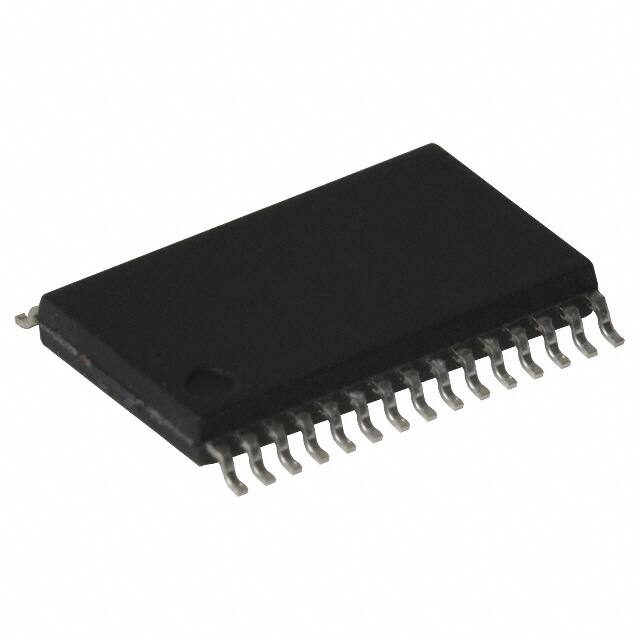
The TC78B041FNG adopts SSOP30 type package.
The TC78B042FTG adopts QFN32 type package, adding RESX
and VREF2 pins.
Features
•
Sine-wave PWM control
•
Automatic lead angle control (InPAC: Intelligent Phase
Control)
•
Lead angle control with external input
•
Hall sensor input/Hall IC input
•
Forward rotation/Reverse rotation switch
•
Number of pulses of rotation pulse signal output is selectable.
•
Output current can be limited.
•
Built-in regulator circuit (VREF= 5 V (typ.), 35 mA (max))
•
Operating supply voltage range: VCC = 6 V to 16.5 V
•
Built-in motor lock detection
© 2017-2019
Toshiba Electronic Devices & Storage Corporation
SSOP30-P-300-0.65
Weight: 0.18 g (typ.)
P-VQFN32-0505-0.50-005
Weight: 0.06 g (typ.)
1
2019-4-12
�TC78B041FNG/TC78B042FTG
Block diagram
HUP
VREF VREF2
VCC
5V Regulator
UVLO
UH
HUM
HVP
VH
HVM
WH
HWP
UL
HWM
VL
MODE
WL
CWCCW
RES
RESX
Logic
VSP
LAS
IDC
LA
FGC
AD
Zero
current
detection
LAAJ
LAL
RSI
RSG
FG
Lock
detection
TR
OSC
OSCR
GND
Some of the functional blocks, circuits, or constants in the block diagram may be omitted or simplified for
explanatory purposes.
Note: RESX pin and VREF2 pin are only for the TC78B042FTG.
2
2019-4-12
�TC78B041FNG/TC78B042FTG
Pin assignment: TC78B041FNG (SSOP30)
TR
1
30
CWCCW
OSCR
2
29
UH
MODE
3
28
VH
HWP
4
27
WH
HWM
5
26
UL
HVP
6
25
VL
HVM
7
24
WL
HUP
8
23
GND
HUM
9
22
RSG
VREF
10
21
RSI
LAAJ
11
20
IDC
LA
12
19
LAS
LAL
13
18
RES
FG
14
17
VCC
FGC
15
16
VSP
3
2019-4-12
�TC78B041FNG/TC78B042FTG
Pin description: TC78B041FNG (SSOP30)
Pin No.
Pin symbol
Description
1
TR
2
OSCR
Setting internal oscillation frequency
3
MODE
Input pin for selecting VSP setting
4
HWP
W-phase hall-signal input (+)
5
HWM
W-phase hall-signal input (-)
6
HVP
V-phase hall-signal input (+)
7
HVM
V-phase hall-signal input (-)
8
HUP
U-phase hall-signal input (+)
9
HUM
U-phase hall-signal input (-)
10
VREF
5V-reference voltage output pin
11
LAAJ
Input pin for adjusting auto lead angle
12
LA
Input pin for setting lead angle
13
LAL
Input pin for setting VSP lead angle limit
14
FG
Output pin for rotation pulse
15
FGC
Input pin for selecting FG pin setting
16
VSP
Input pin for rotation speed control voltage
17
VCC
Power supply voltage pin
18
RES
Input pin for error detection (positive)
19
LAS
Input pin for selection: Sine-wave generation, Lead angle function
20
IDC
Input pin for limiting output current
21
RSI
Input pin for detecting auto lead angle
22
RSG
Reference pin for detecting auto lead angle
23
GND
Ground pin
24
WL
W-phase output pin (low-side commutation signal)
25
VL
V-phase output pin (low-side commutation signal)
26
UL
U-phase output pin (low-side commutation signal)
27
WH
W-phase output pin (high-side commutation signal)
28
VH
V-phase output pin (high-side commutation signal)
29
UH
U-phase output pin (high-side commutation signal)
30
CWCCW
Setting motor lock detection
Input pin for controlling forward/reverse rotation
4
2019-4-12
�TC78B041FNG/TC78B042FTG
Pin assignment: TC78B042FTG (QFN32)
VH
WH
UL
22
UH
23
CWCCW
OSCR
24
TR
MODE
21
20
19
18
17
HVP
27
14
GND
HVM
28
13
RSG
HUP
29
12
RSI
HUM
30
11
IDC
VREF
31
10 VREF2
LAAJ
32
9
1
2
3
4
5
6
7
8
RESX
WL
RES
15
VCC
26
VSP
HWM
FGC
VL
FG
16
LAL
25
LA
HWP
LAS
The exposed metal portion of the back side (E-PAD: size 3.3 mm×3.3 mm) should be connected to GND
because it is connected to the back of the internal chip electrically.
5
2019-4-12
�TC78B041FNG/TC78B042FTG
Pin description: TC78B042FTG (QFN32)
Pin No.
Pin symbol
Description
1
LA
Input pin for setting lead angle
2
LAL
Input pin for setting VSP lead angle limit
3
FG
Output pin for rotation pulse
4
FGC
Input pin for selecting FG pin setting
5
VSP
Input pin for rotation speed control voltage
6
VCC
Power supply voltage pin
7
RES
Input pin for error detection (positive)
8
RESX
Input pin for error detection (negative)
9
LAS
10
VREF2
5V-reference voltage output pin 2
11
IDC
Input pin for limiting output current
12
RSI
Input pin for detecting auto lead angle
13
RSG
Reference pin for detecting auto lead angle
14
GND
Ground pin
15
WL
W-phase output pin (low-side commutation signal)
16
VL
V-phase output pin (low-side commutation signal)
17
UL
U-phase output pin (low-side commutation signal)
18
WH
W-phase output pin (high-side commutation signal)
19
VH
V-phase output pin (high-side commutation signal)
20
UH
U-phase output pin (high-side commutation signal)
21
CWCCW
22
TR
23
OSCR
Setting internal oscillation frequency
24
MODE
Input pin for selecting VSP setting
25
HWP
W-phase hall-signal input (+)
26
HWM
W-phase hall-signal input (-)
27
HVP
V-phase hall-signal input (+)
28
HVM
V-phase hall-signal input (-)
29
HUP
U-phase hall-signal input (+)
30
HUM
U-phase hall-signal input (-)
31
VREF
5V-reference voltage output pin
32
LAAJ
Input pin for adjusting auto lead angle
Input pin for selection: Sine-wave generation, Lead angle function
Input pin for controlling forward/reverse rotation
Setting motor lock detection
6
2019-4-12
�TC78B041FNG/TC78B042FTG
I/O Equivalent circuits
The equivalent circuit diagrams may be simplified or some parts of them may be omitted for explanatory
purposes.
Pin description
Hall signal input
Pin symbol
HUP
HUM
HVP
HVM
HWP
HWM
I/O signal
I/O internal circuit
VREF VREF VREF VREF
Digital filter 18/fosc = 2 μs (typ.)
VREF
VSP
Analog voltage input
Input range: 0 V to 10 V
150 kΩ
Speed control voltage
input
VREF
Internal oscillation
frequency setting
Commutation signal
output
Rotation pulse output
OSCR
Connecting to resistor for setting internal
oscillation frequency
When R = 22 kΩ, fosc = 9.22 MHz (typ.)
UH
VH
WH
UL
VL
WL
VREF
1.2 V
VREF
VREF
Push-pull output (± 2 mA (max))
FG
VCC
5V-reference voltage
output
VREF
VREF: 5 V (typ.) (35 mA (max))
5V-reference voltage
output 2
VREF2
(Note)
VREF2: 5 V (typ.) (3 mA (max))
7
VREF
VREF2
2019-4-12
�TC78B041FNG/TC78B042FTG
Forward/Reverse
control input
Pin symbol
CWCCW
I/O signal
I/O internal circuit
Digital filter 18/fosc = 2 μs (typ.)
100 kΩ
Pin description
H: Reverse (CCW)
L/Open: Forward (CW)
VREF
MODE
Digital filter 18/fosc = 2μs (typ.)
H: VSP input (B mode)
L/Open: VSP input (A mode)
100 kΩ
VSP setting select
input
Digital filter 18/fosc=2μs (typ.)
Select input for FG pin
setting
RESX
(Note)
H/Open: Operation
L: Stop (commutation signal output: Low))
Digital filter 18/fosc = 2 μs (typ.)
H: Stop (commutation signal output: Low)
L/OPEN: Operation
2.5 V
Error detection
negative input
RES
100 kΩ
Error detection positive
input
2.5 V
1 MΩ 100 kΩ
VREF
10-level select input
FGC
Be sure to input voltage in using.
VREF
Lead angle setting
input
32-level select input
LA
Be sure to input voltage in using.
VREF
Select input: sine-wave
generation and lead
angle function
4-level select input
LAS
Be sure to input voltage in using.
8
2019-4-12
�TC78B041FNG/TC78B042FTG
Pin description
Pin symbol
I/O signal
I/O internal circuit
VREF
VSP lead angle limiting
input
16-level select input
LAL
Be sure to input voltage in using.
VREF
Automatic lead angle
adjusting input
64-level select input
LAAJ
Be sure to input voltage in using.
VREF
200 kΩ
IDC
Output current limiting
input
IDC
5 pF
VREF
Digital filter 18/fosc = 2 μs (typ.)
0.5V
RSG
Automatic lead angle
detecting input
Automatic lead angle
detecting for reference
RSI
RSG
When using auto lead angle function, connect
shunt resistor between RSI and RSG.
When auto lead angle function is not used,
connect RSI and RSG to GND.
RSI
VREF
RSG
VREF
Motor lock detection
setting
TR
VREF VREF
Connecting capacitor for motor lock detection
Note: RESX pin and VREF2 pin are only for the TC78B042FTG.
9
2019-4-12
�TC78B041FNG/TC78B042FTG
Absolute maximum ratings (Ta = 25°C)
Characteristics
Symbol
Rating
Unit
Remarks
Power supply voltage
MVCC
18
V
VCC
MVIN1
- 0.3 to 18
V
VSP
MVIN2
- 0.3 to VREF+ 0.3
V
HUP, HVP, HWP, HUM, HVM, HWM,
TR, OSCR, FGC, LA, LAS, LAL, MODE, LAAJ, RES
MVIN3
- 0.3 to 6
V
RESX, CWCCW
MVIN4
VREF+ 0.3
V
IDC, RSI
MVout1
6
V
VREF, VREF2
MVout2
- 0.3 to VREF+ 0.3
V
FG, UH, VH, WH, UL, VL, WL
Output current
MIOUT
2
mA
FG, UH, VH, WH, UL,VL, WL
VREF output current
MIrefout
35
mA
VREF (VREF+VREF2)(Note)
(VREF2 output current is also included.)
VREF2 output current
MIrefout2
3
mA
VREF2 (Note)
P D1
1.87
W
TC78B041FNG (SSOP30)
When mounted on JEDEC 4-layer board
P D2
4.25
W
TC78B042FTG (QFN32)
When mounted on JEDEC 4-layer board
Input voltage
Output voltage
Power dissipation
Operating temperature
Topr
- 40 to 115
°C
Operating temperature range is determined according
to the characteristics of power dissipation. The
maximum junction temperature should not exceed Tj
(max) (150°C).
Storage temperature
Topr
- 55 to 150
°C
―
The absolute maximum ratings of a semiconductor device are a set of ratings that must not be exceeded, even for
a moment.
Do not exceed any of these ratings. Exceeding the rating (s) may cause the device breakdown, damage or
deterioration, and may result injury by explosion or combustion.
Please use the IC within the specified operating ranges.
Note: VREF2 pin is only for the TC78B042FTG.
10
2019-4-12
�TC78B041FNG/TC78B042FTG
Operating ranges (Ta = 25°C)
Characteristics
Symbol
Min
Typ.
Max
Unit
Remarks
Power supply voltage
VCCopr
6
15
16.5
V
VCC
Oscillation frequency
fOSCopr
6.8
9.22
15.5
MHz
―
VSPopr
0
―
7.3
V
VSP: Normal control
VSPoprT
8.2
―
10
V
VSP: Test mode
Speed control voltage input
Power dissipation (for reference only)
PD – Ta
(1)
(W)
4-layer board,
Rth (j-a) = 66.9°C/W.
(2) IC only
Rth (j-a) = 145°C/W
1.2
0.8
(2)
0.4
0
0
When mounted on JEDEC
(1)When mounted on JEDEC
Power dissipation PD
(W)
Power dissipation PD
1.6
PD – Ta
5
2.0
50
100
150
200
Ambient temperature Ta (°C)
TC78B041FNG (SSOP30)
4-layer board,
4
Rth (j-a) = 29.4°C/W.
3
2
1
0
0
50
100
150
200
Ambient temperature Ta (°C)
TC78B042FTG (QFN32)
11
2019-4-12
�TC78B041FNG/TC78B042FTG
Electrical characteristics (Unless otherwise specified, Ta = 25°C and VCC = 15 V)
Characteristics
Symbol
Supply current
ICC
Input current
Min
Typ.
Max
Unit
VREF = OPEN
2
5
8
mA
IIN1
VIN = 5 V:CWCCW, MODE, RESX
25
50
100
IIN2
VIN = 0 V:FGC, LA, LAS, LAL, LAAJ
-1
0
1
IIN3
VIN = 5 V:VSP
17
33
70
IIN4
VIN = 0 V:RES
-100
-50
-25
IIN5
VIN = 5 V:RES
-2
5
10
H
CWCCW, MODE
2
―
―
L
CWCCW, MODE
0
―
0.8
VIN1
―
±0.1
―
HVTH RES, RESX
―
2.6
2.7
LVTH RES, RESX
2.3
2.4
―
Hys
VIN2
VSPA
VSPB
Hall sensor
inputs
CWCCW, MODE (Reference value)
RES, RESX (Reference value)
―
±0.1
―
T
PWM Max, ON duty → Test mode
7.3
7.75
8.2
H
Motor operation → PWM Max, ON duty
5.1
5.4
5.7
M
Refresh → Output Duty operation start
1.8
2.1
2.4
Hys
Input voltage
AD input voltage STEP width
Test Condition
L
Commutation OFF → Refresh
0.7
1.0
1.3
T
PWM Max, ON duty → Test mode
7.3
7.75
8.2
H
Motor operation → PWM Max, ON duty
4.7
5
5.3
M
Refresh → Output Duty operation start
μA
V
V
V
V
0.1
0.2
0.3
VAD4
LAS (Reference value)
1.125
1.25
1.325
V
VAD16
LAL, FGC (Reference value)
0.281
0.313
0.331
V
VAD32
LA (Reference value)
0.141
0.156
0.166
V
VAD64
LAAJ (Reference value)
0.070
0.078
0.083
V
Input sensitivity
VS
Differential inputs
40
―
―
mVpp
Common-mode
input voltage
VW
―
0.2
―
3.5
V
Input hysteresis
VHhys
(Reference value)
±1.5
±7.5
±13.5
mV
VREF
-1
―
VREF
0
―
0.8
Hall IC input
VHIN
H
HUP, HVP, HWP: HUM, HVM, HWM = VREF/2
L
Thallr
HUP, HVP, HWP = Hall IC input,
HUM, HVM, HWM = VREF/2, OSCR = 22 kΩ
UH, VH, WH, UL, VL, WL, FG: Rising (Reference value)
―
4
―
μs
Thalf
HUP, HVP, HWP = Hall IC input,
HUM, HVM, HWM = VREF/2, OSCR = 22 kΩ
UH, VH, WH, UL, VL, WL, FG: Falling (Reference value)
―
2
―
μs
VREF
- 0.78
VREF
- 0.3
―
Input delay time
Output voltage
Output leakage current
V
VOUTH
IOUT = -2 mA: UH, VH, WH, UL, VL, WL, FG
VOUTL
IOUT = 2 mA: UH, VH, WH, UL, VL, WL, FG
―
0.3
0.78
VREFA
VREF = 0 mA: VREF, (VREF2 = OPEN) (Note1)
4.7
5.0
5.3
VREFB
VREF = -15 mA: VREF, (VREF2 = OPEN) (Note1)
4.7
5.0
5.3
VREFC
VREF = -35 mA: VREF, (VREF2 = OPEN) (Note1)
4.5
5.0
5.3
VREF2A
VREF2 = 0 mA: VREF2, (VREF = OPEN) (Note1)
4.7
5.0
5.3
VREF2B
VREF2 = -3 mA: VREF2, (VREF = -12 mA) (Note1)
4.7
5.0
5.3
VREF2C
VREF2 = -3 mA: VREF2, (VREF = -32 mA) (Note1)
4.5
5.0
5.3
ILH
VOUT = 0 V: UH, VH, WH, UL, VL, WL, FG
―
0
1
ILL
VOUT = 5 V: UH, VH, WH, UL, VL, WL, FG
―
0
1
12
2019-4-12
V
μA
�TC78B041FNG/TC78B042FTG
Characteristics
Symbol
Output OFF time
(Dead time)
VOFF(18)
OSCR = 22 kΩ IOUT = 2 mA (Reference value)
VOFF(20)
Oscillation frequency
PWM oscillation frequency
(Carrier frequency)
Test Condition
Min
Typ.
Max
Unit
1.7
2
2.3
μs
OSCR = 20 kΩ IOUT = 2 mA (Reference value)
1.5
1.79
2.07
μs
fosc(18)
OSCR = 22 kΩ (Reference value)
8.29
9.22
10.14
MHz
fosc(20)
OSCR = 20 kΩ (Reference value)
9.06
10.06
11.08
MHz
FC(18)
OSCR = 22 kΩ (Reference value)
16.2
18
19.8
kHz
FC(20)
OSCR = 20 kΩ (Reference value)
17.7
19.6
21.7
kHz
Maximum conduction duty
width
(Sine wave)
TON180MAX (Reference value)
(Note2)
96.3
(Note2)
%
Maximum conduction duty
width
(120°commutation)
TON120MAX (Reference value)
(Note2)
85
(Note2)
%
―
0.2
―
%
0.48
0.5
0.52
V
μs
Minimum conduction duty
width
TONMIN
Output current limiting voltage
VIDC
IDC
Input delay of current
detection
TIDC
IDC OSCR = 22 kΩ (Reference value)
―
3.2
―
VCC(H)
Output turn-on threshold
5.0
5.5
5.9
VCC monitor
VREF monitor
Motor lock detection
Current detection accuracy of
auto lead angle
(Reference value)
VCC(L)
Output turn-off threshold
4.5
5
5.5
VCC(H)
Input voltage hysteresis (Reference value)
―
0.5
―
V
VREF(H)
Output turn-on threshold
3.7
4
4.3
VREF(L)
Output turn-off threshold
3.4
3.7
4
VREF(H)
Input voltage hysteresis (Reference value)
―
0.3
―
TONTR
TR = 0.01 μF Operation period (Reference value)
3.7
5
7.4
s
TOFFTR
TR = 0.01 μF Output disabled period (Reference value)
22.2
30
44.4
s
V
FTR
TR = 0.01 μF frequency
68
100
132
Hz
ICTR
Charge current (Reference value)
2
3
4
μA
IDTR
Discharge current (Reference value)
-4
-3
-2
μA
VHTR
High-side threshold (Reference value)
2.7
3
3.3
V
VLTR
Low-side threshold (Reference value)
1.35
1.5
1.65
V
VRS
(Reference value)
-1
0
1
mV
Reference value: Design values. No shipping inspection.
Note1: VREF2 pin is only for the TC78B042FTG.
Note2: Since the output Duty is controlled by the logic circuit, the maximum and minimum values of the
maximum conduct duty width are the same with typical values, and these values are design values.
However, the values may be different from the typical values due to a delay of the load capacity, etc.
13
2019-4-12
�TC78B041FNG/TC78B042FTG
Functional description
1. Basic operation
At startup, the motor is driven with 120° commutation. When the hall signal indicates a rotation speed (f) of
1 Hz or more, the motor rotates by estimating the rotor position. (Note)
0 (Startup) ≤ f < 1 Hz: Square-wave drive (120° commutation)
1Hz ≤ f: Sine-wave PWM drive (180° commutation)
Note: When oscillation frequency (fosc) is 9.22 MHz, the switching period from the hall signal to the
following one is about 0.167 s. Then, the frequency for one cycle is about 1 Hz ((6×1536000)/fosc).
When f is 1 Hz or more, the motor is driven according to the command of the LA pin.
When f is less than 1Hz or the motor rotation direction is reverse (according to the timing chart),
the motor is driven with 120° commutation (lead angle is 0°).
2. Reference clock and carrier frequency setting
Reference clock (oscillation frequency: fosc) is determined by the resistance (R) of the OSCR pin. It
configures PWM frequency (carrier frequency). The calculating formula is shown below. When the resistance
(R) of the OSCR pin is 22 kΩ, oscillation frequency is 9.22 MHz (typ.) and carrier frequency is 18 kHz (typ.).
Carrier frequency: FC = fosc /512 (Hz)
OSCR pin
resistor value [kΩ]
Reference clock
fosc[MHz] (typ.)
PWM frequency (carrier frequency)
Fc[kHz] (typ.)
27
7.62
14.9
24
8.5
16.6
22
9.22
18
20
10.06
19.6
18
11.08
21.6
16
12.33
24.1
15
13.07
25.5
3. Dead time insertion (cross conduction protection)
To prevent a short-circuit between external low-side and high-side power devices during sine-wave PWM
drive, a dead time is digitally inserted. (The dead time is also implemented at the full duty cycle during
square-wave drive.)
Td = 18/fosc
Td ≈ 2 μs when fosc ≈ 9.22 MHz, where
fosc is reference clock frequency
(Oscillation frequency).
UH
(VH, WH)
UL
(VL, WL)
14
Td
Td
2019-4-12
�TC78B041FNG/TC78B042FTG
4. Hall signal
Common-mode input voltage range: VW = 0.2 V to 3.5 V
Input hysteresis: VHhys = 7.5 mV (typ.)
HUM
VS
VHhys = +7.5 mV (typ.)
VHhys = -7.5 mV (typ.)
HUP
VS = 40 mV or more
Usage setting example 1: HUP, HVP, HWP =GND to VREF: HUM, HVM, HWM=VREF/ 2
Usage setting example 2: HUP, HVP, HWP =VREF/ 2: HUM, HVM, HWM=GND to VREF
15
2019-4-12
�TC78B041FNG/TC78B042FTG
5. Rotation pulse output
The IC outputs rotating pulse based on the hall signal. FGC pin can switch number of pulses. One pulse per
electrical angle is generated from the hall signal of U phase. 3 pulses per electrical angle are generated by
combining each rising and falling edge of U, V, and W phases.
2.4 or 2 or 0.8 pulses per electrical angle are generated by rotating the motor with 1.5 electrical angle under
the condition that the frequency of the hall signal (U phase) is about 0.68 Hz or higher (condition: fosc = 9.22
MHz). They are not generated when f is less than 0.68 Hz. Since the pulses are not generated synchronous
with hall signal switching edge, each phase of hall signal cannot be judged by FG signal.
In STEP8, output timing of commutation signal is enabled. Approximate lead angle can be calculated as
follows; Lead angle (°) = (0.6×Duty (%))-0.94.
STEP
FGC[V]
(Note)
FG
0
0.00
3 pulses/electrical angle
1
0.31
2
0.63
3
0.94
4
1.25
5
1.56
6
1.88
7
2.19
Test mode 1
8
2.50
Test mode 2: Lead angle timing
9
2.81
1 pulse/electrical angle
2.4 pulses/electrical angle
2 pulses/electrical angle
0.8 pulses/electrical angle
Note: The threshold voltage of the FGC pin is a typical value. The value is configured based on VREF pin
voltage, so that it fluctuates with VREF pin voltage.
HUM
1 electrical angle
HUP
HVM
HVP
HWP
HWM
STEP0
STEP1/2
STEP3/4
STEP5/6
Duty1
Duty2
STEP8
Example 1:When Duty1 = about 40%, Lead angle = about 23°
Example 2:When Duty2 = about 60%, lead angle = about 35°
STEP9
Note: Above timing chart is an example and simplified for explanatory purposes. The 2.4, 2, and 0.8 pulses or
electrical angle may not be synchronized with hall signals.
16
2019-4-12
�TC78B041FNG/TC78B042FTG
6. Setting rotation speed control
By changing the input voltage of VSP pin, duty of the commutation signal output is changed and the motor
rotation speed can be controlled.
Input mode of VSP pin can be selected between A and B by using MODE pin.
MODE pin
High
Low/OPEN
Input type of VSP pin
B mode
A mode
(1)
Voltage command input: VSP ≤1.0 V
The commutation signal outputs are disabled (i.e., gate block protection is activated).
(2)
Voltage command input: 1.0 V < VSP ≤2.1 V (Refresh)
The low-side commutation signal is turned on for a constant period (carrier period). ON duty: about 8%
(40/fosc)
(3)
Voltage command input: 2.1 V < VSP ≤ 7.75 V
Output ON duty is changed by setting 256-resolution. When VSP is 5.4 V (typ.) or more, output ON duty
keeps the maximum value.
During square-wave drive, the low-side commutation signal is turned on forcedly for a constant period
(carrier period). ON duty: about 8% (40/fosc)
In stop mode (Rotation frequency < 1 Hz when fosc=9.22 MHz), the commutation signal is output after
VSP exceeds 2.1 V and the refresh mode is activated for 1.5 ms (condition: fosc=9.22 MHz). In rotation
mode (Rotation frequency ≥ 1 Hz when fosc=9.22 MHz), the commutation signal is output immediately
after VSP exceeds 2.1 V.
Note: In startup, low-side commutation signal should be turned on (1.0 V < VSP ≤2.1 V) for a certain
period to charge the high-side gate power supply.
(4)
Voltage command input: 7.75 V < VSP ≤ 10 V (test mode for motor shipping)
In sine-wave drive mode, the motor rotates with lead angle of zero.
Output ON duty keeps the maximum value.
Note: In the test mode for motor shipment, even if the setting of the sine wave generation method is the
sine-wave 360° reset with the LAS pin, the setting is the sine-wave 60° reset
PWM Duty
Max
1.0 V
(1)
2.1 V
5.4 V
(3)
(2)
7.75 V
10 V
Vsp
(4)
Note: The threshold voltage in each state of the VSP pin is a typical value. The value is configured based on
VREF pin voltage, so that it fluctuates with VREF pin voltage.
17
2019-4-12
�TC78B041FNG/TC78B042FTG
(1)
Voltage command input: VSP ≤ 0.2 V (Refresh)
The low-side commutation signal is turned on for a constant period (carrier period). ON duty: about 8%
(40/fosc)
(2)
Voltage command input: 0.2 V < VSP ≤ 7.75 V
Output ON duty is changed by setting 256-resolution. When VSP is 5 V (typ.) or more, output ON duty
keeps the maximum value.
During square-wave drive, the low-side commutation signal is turned on forcedly for a constant period
(carrier period). ON duty: about 8% (40/fosc)
In stop mode (Rotation frequency < 1 Hz when fosc=9.22 MHz), the commutation signal is output after
VSP exceeds 0.2 V and the refresh mode is activated for 1.5 ms (condition: fosc=9.22 MHz). In rotation
mode (Rotation frequency ≥ 1 Hz when fosc=9.22 MHz), the commutation signal is output immediately
after VSP exceeds 0.2 V.
Note: In startup, low-side commutation signal should be turned on (0.2 V < VSP) for a certain period to
charge the high-side gate power supply.
(3)
Voltage command input: 7.75 V < VSP ≤ 10 V (test mode for motor shipping)
In sine-wave drive mode, the motor rotates with lead angle of zero.
Output ON duty keeps the maximum value.
Note: In the test mode for motor shipment, even if the setting of the sine wave generation method is the
sine-wave 360° reset with the LAS pin, the setting is the sine-wave 60° reset.
PWM Duty
MAX
0.2 V
(1)
5V
(2)
7.75 V
10 V
VSP
(3)
Note: The threshold voltage in each state of the VSP pin is a typical value. The value is configured based on
VREF pin voltage, so that it fluctuates with VREF pin voltage.
18
2019-4-12
�TC78B041FNG/TC78B042FTG
7. Setting lead angle function and sine-wave generation
LAS pin can set sine-wave generation and lead angle function. Details are shown below.
STEP
LAS voltage [V]
(Note)
Sine-wave generation
Lead angle function
LA pin setting
0
0
Sine-wave (60°) reset
Automatic
(InPAC: Intelligent Phase Control)
Lead angle upper limit setting of
the current limiting lead angle
0° to 58° / 32 steps
1
1.25
Sine-wave (360°) reset
Automatic
(InPAC: Intelligent Phase Control)
Lead angle upper limit setting of
the current limiting lead angle
0° to 58° / 32 steps
2
2.5
Sine-wave (360°) reset
External input
Set phase of commutation signal
output:
0° to 58° / 32 steps
3
3.75
Sine-wave (60°) reset
External input
Set phase of commutation signal
output:
0° to 58° / 32 steps
Note: The threshold voltage of the LAS pin is a typical value. The value is configured based on VREF pin voltage,
so that it fluctuates with VREF pin voltage.
(1)
Automatic lead angle control function (InPAC: Intelligent Phase Control)
The auto lead angle control function corrects based on the input signal of hall signal so that zero-cross point of
U-phase output current is 0° position in the following timing chart. It detects an output current at the
position of 0° in the timing chart, and the phase is judged once per one electrical angle, whether the lead
angle or delay angle. When the result judged 4 times continuously is matched, it changes the phase (range: 0°
to 58°) of a commutation signal output for each step (0.94°), and corrects the zero crossing position of output
current. If the result is not matched, the phase of commutation signal does not change.
Additionally, the auto lead angle control function corrects the zero-cross point of U-phase output current to 0°
position of the timing chart when the phase relation between U phase hole signal and U phase Back-EMF is
the following timing chart. Therefore, motor driving efficiency is optimized when zero-cross point of U-phase
Back-EMF and U-phase output current are corresponded. Since zero-cross point of the output current is
detected by RSI and RSG pins through shunt resistor, connection of RSI pin and RSG pin via the shunt
resistor is required to apply auto lead angle function.
Moreover, rotation speed (i.e. one electrical angular frequency of hall signal) that enables normal auto lead
angle control has a limit (Finpac). The limit value (Finpac) is determined according to PWM frequency
(carrier frequency) and phase correction value. It can be calculated by the formula of ‘Finpac=PWM
frequency×{(30+phase)/540}’. When the rotation speed exceeds this limit value, auto lead angle function may
not work.
Example: In case of PWM frequency = 16.2 kHz, phase (LAAJ pin function) = 0° setting, Finpac = 900 Hz.
19
2019-4-12
�TC78B041FNG/TC78B042FTG
(Non inverted hall signal input) 1 electrical angle
HUM
HUP
HVM
HVP
HWP
HWM
Back-EMF
V phase
U phase
W phase
1 Hz < Hall signal input frequency
(180°commutation: Modulated waveforms in the IC)
Su
Phase is changed automatically.
Phase is changed automatically.
UH
UL
U-phase output current
Iu
LAAJ pin: Phase correction value
+30°
0°
+30°
20
0°
2019-4-12
�TC78B041FNG/TC78B042FTG
(Inverted hall signal input)
1 electrical angle
HUM
HUP
HVM
HVP
HWP
HWM
Back-EMF
W phase
U phase
V phase
1 Hz < Hall signal input
(180°commutation: Modulated waveforms in the IC)
Su
Phase is changed automatically.
Phase is changed automatically.
UH
UL
U-phase output current
Iu
LAAJ pin: Phase correction value +30°
0°
+30°
21
0°
2019-4-12
�TC78B041FNG/TC78B042FTG
In the auto lead angle setting (InPAC), when the current limiting (IDC pin function) works at the zero-cross
detecting point of output current and does not judge the auto lead angle (InPAC) phase, the current limiting
lead angle (IDC lead angle) advances the lead angle. The LA pin is set to the upper limit value of current
limiting lead angle (IDC lead angle).
In the auto lead angle setting (InPAC), when the current limiting (IDC pin function) works at zero-cross
detecting point of output current, the phase judgement cannot be performed and the auto lead angle control
(InPAC) cannot work. However, in this case, the lead angle can be advanced by the current limiting lead angle
function (IDC lead angle). Whenever the state where the auto lead angle (InPAC) cannot perform a phase
judgement by the current limiting counts 4 times, the lead angle of 1 step (0.94°) is advanced. The lead angle
counts by the auto lead angle control (InPAC) are reset when the auto lead angle control (InPAC) does not
perform the phase judgement by current limiting.
The LA pin can set the upper limit value of current limiting lead angle not to advance too much the lead angle
by this current limiting lead angle function.
The upper limit setting of the LA pin lead angle is only for the setting of this current limiting lead angle
function (IDC lead angle), so that normal auto lead function setting (InPAC) cannot be set this limit value
arbitrary. The upper limit value is 58.1°.
0
LA voltage [V]
(Note)
0.00
1
0.16
1.9
17
2.66
31.9
2
0.31
3.8
18
2.81
33.8
3
0.47
5.6
19
2.97
35.6
4
0.63
7.5
20
3.13
37.5
5
0.78
9.4
21
3.28
39.4
6
0.94
11.3
22
3.44
41.3
7
1.09
13.1
23
3.59
43.1
8
1.25
15.0
24
3.75
45.0
9
1.41
16.9
25
3.91
46.9
10
1.56
18.8
26
4.06
48.8
11
1.72
20.6
27
4.22
50.6
12
1.88
22.5
28
4.38
52.5
13
2.03
24.4
29
4.53
54.4
14
2.19
26.3
30
4.69
56.3
15
2.34
28.1
31
4.84
58.1
STEP
Lead angle [°]
STEP
0.0
16
LA voltage [V]
(Note)
2.50
Lead angle [°]
30.0
Note: The threshold voltage of the LA pin is a typical value. The value is configured based on VREF pin
voltage, so that it fluctuates with VREF pin voltage.
22
2019-4-12
�TC78B041FNG/TC78B042FTG
(2)
Lead angle set by external input
Lead angle of commutation signal output against hall signal can be fixed by LA input voltage.
0
LA voltage [V]
(Note)
0.00
1
0.16
1.9
17
2.66
31.9
2
0.31
3.8
18
2.81
33.8
3
0.47
5.6
19
2.97
35.6
4
0.63
7.5
20
3.13
37.5
5
0.78
9.4
21
3.28
39.4
6
0.94
11.3
22
3.44
41.3
7
1.09
13.1
23
3.59
43.1
8
1.25
15.0
24
3.75
45.0
9
1.41
16.9
25
3.91
46.9
10
1.56
18.8
26
4.06
48.8
11
1.72
20.6
27
4.22
50.6
12
1.88
22.5
28
4.38
52.5
13
2.03
24.4
29
4.53
54.4
14
2.19
26.3
30
4.69
56.3
15
2.34
28.1
31
4.84
58.1
STEP
Lead angle [°]
STEP
0.0
16
LA voltage [V]
(Note)
2.50
Lead angle [°]
30.0
Note: The threshold voltage of the LA pin is a typical value. The value is configured based on VREF pin
voltage, so that it fluctuates with VREF pin voltage.
23
2019-4-12
�TC78B041FNG/TC78B042FTG
Lead angle limit function (LAL pin setting)
When VSP input voltage is too low to provide enough output current, zero-cross point of output current
cannot be detected accurately and auto lead angle function may not work properly because this function is
activated by detecting zero-cross point of the output current. In this case, lead angle limit function is applied.
In the auto lead angle function setting, when the input voltage (input Duty) of the VSP pin in the following
LAL pin setting is less than the setting value, the auto lead angle limiting function is fixed angle of the LAL
pin setting without working. As the fixed lead angle value is an initial value, a sine wave of the lead angle
value also starts from this fixed lead angle value when changing from a rectangle wave to a sine wave. When
the VSP pin voltage exceeds the configured voltage, the auto lead angle control function works and changes
from the fixed lead angle to a suitable lead angle by 1 step (0.94°). Moreover, in external input setting, auto
lead angle function using LAL pin is not enabled.
STEP
LAL voltage
[V]
(Note)
Fixed lead
angle [°]
(Initial
value)
0
0.00
1
VSP voltage [V] / A mode (Note)
VSP voltage [V] / B mode (Note)
(VSP input: conversed to duty)
(VSP input: conversed to duty)
Hysteresis
VSP increase
side
Hysteresis
VSP decrease
side
Hysteresis
VSP increase
side
Hysteresis
VSP decrease
side
No limit
(0°)
―
―
―
―
0.31
5.6
2.49 V or less
2.43 V or less
0.77 V or less
0.68 V or less
2
0.63
0
(12% or less)
(10% or less)
(12% or less)
(10% or less)
3
0.94
11.3
4
1.25
5.6
2.66 V or less
2.60 V or less
1.01 V or less
0.92 V or less
5
1.56
0
(17% or less)
(15% or less)
(17% or less)
(15% or less)
6
1.88
12.2
7
2.19
6.6
2.83 V or less
2.76 V or less
1.27 V or less
1.17 V or less
8
2.50
0
(22% or less)
(20% or less)
(22% or less)
(20% or less)
2.99 V or less
2.93 V or less
1.51 V or less
1.41 V or less
(27% or less)
(25% or less)
(27% or less)
(25% or less)
9
2.81
13.1
10
3.13
7.5
11
3.44
0
12
3.75
18.8
13
4.06
13.1
3.15 V or less
3.09 V or less
1.74 V or less
1.64 V or less
14
4.38
7.5
(32% or less)
(30% or less)
(32% or less)
(30% or less)
15
4.69
0
Note: The threshold voltage of the LAL pin and VSP pin is typical values. The values are configured based on
VREF pin voltage, so that they fluctuate with VREF pin voltage.
24
2019-4-12
�TC78B041FNG/TC78B042FTG
Automatic lead angle correction (LAAJ pin setting)
LAAJ pin can correct zero-cross point of output current during auto lead angle control as well as LA pin.
Configuration is shown below.
STEP
LAAJ [V]
Phase
[°]
STEP
LAAJ [V]
Phase
[°]
STEP
LAAJ [V]
Phase
[°]
STEP
LAAJ [V]
Phase
[°]
0
0.00
0.0
16
1.25
8.4
32
2.50
23.4
48
3.75
30.0
1
0.08
0.0
17
1.33
9.4
33
2.58
24.4
49
3.83
30.0
2
0.16
0.0
18
1.41
10.3
34
2.66
25.3
50
3.91
30.0
3
0.23
0.0
19
1.48
11.3
35
2.73
26.3
51
3.98
30.0
4
0.31
0.0
20
1.56
12.2
36
2.81
27.2
52
4.06
30.0
5
0.39
0.0
21
1.64
13.1
37
2.89
28.1
53
4.14
30.0
6
0.47
0.0
22
1.72
14.1
38
2.97
29.1
54
4.22
30.0
7
0.55
0.0
23
1.80
15.0
39
3.05
30.0
55
4.30
30.0
8
0.63
0.9
24
1.88
15.9
40
3.13
30.0
56
4.38
30.0
9
0.70
1.9
25
1.95
16.9
41
3.20
30.0
57
4.45
30.0
10
0.78
2.8
26
2.03
17.8
42
3.28
30.0
58
4.53
30.0
11
0.86
3.8
27
2.11
18.8
43
3.36
30.0
59
4.61
30.0
12
0.94
4.7
28
2.19
19.7
44
3.44
30.0
60
4.69
30.0
13
1.02
5.6
29
2.27
20.6
45
3.52
30.0
61
4.77
30.0
14
1.09
6.6
30
2.34
21.6
46
3.59
30.0
62
4.84
30.0
15
1.17
7.5
31
2.42
22.5
47
3.67
30.0
63
4.92
30.0
Note: The threshold voltage of the LAAJ pin is a typical value. The value is configured based on VREF pin voltage,
so that it fluctuates with VREF pin voltage.
25
2019-4-12
�TC78B041FNG/TC78B042FTG
(1)
Reset of sine-wave (60°)
Hall signals generated from hall sensors are modulated, and a sinusoidal PWM waveform is created by
comparing the modulated waveform to a triangular waveform.
The counter measures the period from a rising edge (falling edge) of each hall signal to its next falling edge
(rising edge) (corresponding to the electrical angle of 60°). This period is then used as 60° phase data for the
next modulation. A total of 64 ticks comprise 60° phase data. The time width of a tick equals 1/64th the time
width of the immediately preceding 60° phase.
HU
(6)
(1)
(3)
HU, HV, HW: Hall signal (Note)
HV
(5)
(2)
HW
(6)’
(1)’
(2)’
(3)’
Su
Sv
Sw
In the above diagram, the modulated waveforms have an interval (1)’ that is equal to the time width between
a rising edge of HU to a falling edge of HW (1) of the previous cycle. In the same way, the modulated
waveforms have an interval (2)’ that is equal to the time width between a falling edge of HW to a rising edge
of HV (2) of the previous cycle. If next edge does not appear before 64 ticks end, next 64 ticks become equal to
the next period until the next edge appear.
*t
64
63
62
1
Su
2
3
4
5
6
(2)’
* t = t (2) × 1/64
64 data
Phase matching between the hall signal and the modulated waveform is carried out for every zero-cross point
of the hall signal. Modulation is reset on each rising edge and falling edge of the hall signal for every 60
electrical degrees. Therefore, when the hall sensor is displaced or the motor is accelerating or decelerating,
the modulated waveform becomes discontinuous upon each reset.
Note: Square waveforms are used in the above diagram for the sake of simplicity.
26
2019-4-12
�TC78B041FNG/TC78B042FTG
(2)
Reset of sine-wave (360°)
Hall signals generated from hall sensors are modulated, and a sinusoidal PWM waveform is created by
comparing the modulated waveform to a triangular waveform.
The counter measures the period from a falling edge of HU to its next falling edge (corresponding to the
electrical angle of 360°). This period is then used as 360° phase data for the next modulation.
A total of 384 ticks comprise 360° phase data. The time width of a tick equals 1/384th the time width of the
immediately preceding 360° phase.
(Note)
HU
T1
T2
T1’
T2’
Su
Sv
Sw
T1’ = T1
T2’ = T2
In the above diagram, the modulated waveforms have an interval (T1’) that is equal to the time width
between a falling edge of HU to the next falling edge of HU (T1) of the previous cycle. If next edge does not
appear before T1’ data ends, next T1’ data becomes equal to the next period until the next edge appear.
Modulation is reset on each falling edge of the hall signal for every 360 electrical degrees. Therefore, when the
motor is accelerating or decelerating, the modulated waveform becomes discontinuous upon each reset.
Note: Square waveforms are used in the above diagram for the sake of simplicity.
27
2019-4-12
�TC78B041FNG/TC78B042FTG
8. Error detections
(1)
Overcurrent protection (IDC pin)
In sine-wave drive, if the IDC pin voltage exceeds the internal reference voltage (0.5 V (typ.)), the
commutation signals are forced to output low level. The current limitation is released for each carrier
frequency.
Note: In auto lead angle setting (InPAC), when the current limiting (IDC pin function) operates at
zero-cross detection point of the output current, the angle leads by the current limiting function.
Refer to the description of LA pin setting.
In square-wave drive, if the IDC pin voltage exceeds the internal reference voltage (0.5 V (typ.)), the
upper phase signals (UH, VH, and WH) are forced to output low level. Lower phase signals (UL, VL,
and WL) are output according to the hall signals as shown in the timing chart. The current limitation
is released for each carrier frequency.
(2)
Error detection positive input (RES pin)
When low level is input to RES pin, the commutation outputs are disabled. When high level is input to
RES pin, the detection function is disabled after every carrier frequency and the commutation
resumes.
In stop mode (Rotation frequency < 1 Hz when fosc=9.22 MHz)), commutation resumes after VSP
exceeds a certain value (A mode: 2.1 V, B mode: 0.2 V) and the refresh function operates for 1.5 ms
(condition: fosc=9.22 MHz).
In rotational mode (Rotation frequency ≥ 1 Hz when fosc=9.22 MHz), commutation resumes after VSP
exceeds a certain value (A mode: 2.1 V, B mode: 0.2 V).
The internal counter is operating and FG signal is output during reset.
(3)
Error detection negative input (RESX pin)
When high level is input to RESX pin, the commutation outputs are disabled. When low level is input
to RESX pin, the detection function is disabled after every carrier frequency and the commutation
resumes.
In stop mode (Rotation frequency < 1 Hz when fosc=9.22 MHz)), commutation resumes after VSP
exceeds a certain value (A mode: 2.1 V, B mode: 0.2 V) and the refresh function operates for 1.5 ms
(condition: fosc=9.22 MHz).
In rotational mode (Rotation frequency ≥ 1 Hz when fosc=9.22 MHz), commutation resumes after VSP
exceeds a certain value (A mode: 2.1 V, B mode: 0.2 V).
The internal counter is operating and FG signal is output during reset.
(4)
Abnormal hall signal protection
When hall signals (internal hall amplifier outputs) are all high or all low levels, the commutation
signals output low level (i.e., gate block protection). When these signals are set to any other
combination, the commutation resumes.
When all of hall inputs (HUP, HUM, HVP, HVM, HWP, and HWM) are set open, the commutation
signals output low level (i.e., gate block protection). When these signals are set to any other
combination, the commutation resumes.
Hall signals (internal hall amplifier outputs) in sine-wave PWM drive have lath type construction.
So, in case the hall signal is output differently from the logic of an expected value, a prior state is held.
Therefore, malfunction may not occur if a slight noise and chattering generate.
28
2019-4-12
�TC78B041FNG/TC78B042FTG
(5)
Under voltage lockout (VCC monitor and VREF monitor)
While the operating voltage is outside the rated range during power-on or power-off, the commutation
outputs are set low level to prevent external power devices from damage due to short-circuits.
When VSP exceeds a certain value (A mode: 2.1 V, B mode: 0.2 V), refresh function is activated for 1.5
ms (condition: fosc=9.22 MHz) and the commutation resumes.
However, since sequence of returning power supply corresponds to the power-on sequence, the circuit
turns into unstable and the operation cannot be guaranteed.
VCC
VCC voltage
5.5 V (typ.)
5.0 V (typ.)
GND
VREF
Commutation signal
(UH, VH, WH, UL, VL, WL)
Output Low
Output enabled
VREF voltage 4 V (typ.)
VREF
Commutatio signal
(UH, VH, WH, UL, VL, WL)
Output Low
Output Low
VREF
3.7 V (typ.)
GND
Output enabled
29
Output Low
2019-4-12
�TC78B041FNG/TC78B042FTG
9. Motor lock detection
Motor lock detection function disables the commutation signals when the motor does not rotate although VSP
exceeds a certain value (A mode: 2.1 V, B mode: 0.2 V) and continues to stop after the drive period (TON (s))
has passed.
Motor lock detection repeats intermitted operation consisted of drive mode and stop mode. The ratio of drive
period: stop period (TOFF(s)) is 1 : 6.
In drive period (TON(s)), when two hall input signal edges are input in the switching order and the time is
less than 0.167s (condition: fosc=9.22 MHz), the motor is in a rotation state and the lock detection state is
released.
When VSP of a certain value or less (A mode: 2.1 V, B mode: 0.2 V) is applied, reset is carried out and the
motor lock detection is released.
After stop period (TOFF(s)), refresh function is activated for 1.5 ms (condition: fosc=9.22 MHz). Then,
commutation resumes.
(1)Non commutating
(Commutation signal output=Low, Refresh
2.1 V ≥ VSP: A mode
0.2 V ≥ VSP: B mode
2.1 V < VSP: A mode
0.2 V < VSP: B mode
(2)Commutating
Rotation speed of hall signal
1 Hz or more
(Condition: fosc=9.22 MHz)
States of (2) to (6)
Rotation speed of hall signal
Less than 1 Hz
(Condition: fosc=9.22 MHz)
(3)Refresh
After stop period (TOFF(s))
1.5 ms or more (Condition: fosc=9.22 MHz)
(4)Motor rotation
(5)Motor stop
Rotation speed of hall signal
1 Hz or more
(Condition: fosc=9.22 MHz)
(6)Motor lock detection
(Commutation signal output: low level
After drive period (TON(s))
Period of drive mode and stop mode (commutation output = low level) can be configured by an external
capacitor (TRC1) of TR pin. They can be calculated as follows;
Drive period (TON(s)) = TRC1 × (VHTR - VLTR) × 2 / I × 500 counts
Stop period (TOFF(s)) = TRC1 × (VHTR - VLTR) × 2 / I × 3000 counts
Example: When TRC1 is 0.01 μF, I(ICTR,IDTR) = 3 μA (typ.), VHTR = 3 V (typ.), and VLTR = 1.5 V (typ.). Then
TON(s) = 5 s (typ.) and TOFF(s) = 30 s (typ.).
30
2019-4-12
�TC78B041FNG/TC78B042FTG
< Use range of TR pin external capacitor and characteristics of motor detection lock>
Item
Symbol
Min
TR pin external capacitor value
TRC1
Motor lock detection frequency
FTR
―
Motor lock detecition enable priod
TON
Motor lock detecition disable period
TOFF
Typ.
Max
Unit
―
F
100
2.1 k
Hz
―
0.23
5
―
s
―
1.4
30
―
s
―
470 p 0.01 μ
Remarks
Open detection may operate if the
capacitor is set less than the minimum
value.
Note1: When TR pin is open, the motor lock detection state is held (commutation signal = low level) by open
detection.
Note2: When TR pin is connected to GND, the motor lock detection is disabled.
31
2019-4-12
�TC78B041FNG/TC78B042FTG
10. Forward/Reverse rotation
Motor rotation direction can be switched by using CWCCW pin. Timing chart is shown as follows;
CWCCW
Hall signal input
Drive method
Timing chart
High
Forward direction
120°commutation
(4)
(Reverse rotation)
Reverse direction
Sin-wave drive
(3)
Low/Open
Forward direction
Sin-wave drive
(1)
(Forward rotation)
Reverse direction
120°commutation
(2)
32
2019-4-12
�TC78B041FNG/TC78B042FTG
(1)
Sine-wave drive timing chart: Forward rotation, Non inverted hall signal input, Lead angle=0°
(CWCCW = Low, FGC = GND)
(Non inverted hall signal input)
HUM
HUP
HVM
HVP
HWP
HWM
Back-EMF
V phase
U phase
W phase
0 < Hall signal input frequency < 1 Hz
(120° commutation)
UH
VH
WH
UL
VL
WL
FG
1 Hz ≤Hall signal input frequency
(180°commutation: Modulated
waveforms in the IC)
Su
Sv
Sw
FG
Note: When the Hall signal input frequency is 1 Hz or more (Condition: fosc = 9.22 MHz), lead angle control is
activated.
The above timing chart is simplified to illustrate the function and behavior of the device.
33
2019-4-12
�TC78B041FNG/TC78B042FTG
(2)
120°commutation drive timing chart: Forward rotation, Inverted hall signal input
(CWCCW = Low, FGC = GND)
(Inverted hall signal input)
HUM
HUP
HVM
HVP
HWP
HWM
Back-EMF
W phase
U phase
V phase
Reverse rotation sensing
(120° commutation)
UH
VH
WH
UL
VL
WL
FG
Note: When CW/CCW = Low and inverted hall signals are input, the IC operates in 120° commutation mode with
a lead angle of 0° (reverse rotation).
The above timing chart is simplified to illustrate the function and behavior of the device.
34
2019-4-12
�TC78B041FNG/TC78B042FTG
(3)
Sine-wave drive timing chart: Reverse rotation, Inverted hall signal input, Lead angle = 0°
(CWCCW = High, FGC = GND)
(Inverted hall signal input)
HUM
HUP
HVM
HVP
HWP
HWM
Back-EMF
W phase
U phase
V phase
0 < Hall signal input frequency < 1 Hz
(120° commutation)
UH
VH
WH
UL
VL
WL
FG
1 Hz ≤ Hall signal input frequency
(180°commutation: Modulated waveforms in the IC)
Su
Sv
Sw
FG
Note: When the Hall signal input frequency is 1 Hz or more (Condition: fosc = 9.22 MHz), lead angle control is
activated.
The above timing chart is simplified to illustrate the function and behavior of the device.
35
2019-4-12
�TC78B041FNG/TC78B042FTG
(4)
120°commutation drive timing chart: Reverse rotation, Non inverted hall signal input
(CWCCW = High, FGC = GND)
(Non inverted hall signal input)
HUM
HUP
HVM
HVP
HWP
HWM
Back-EMF
V phase
U phase
W phase
Reverse rotation sensing
(120° commutation)
UH
VH
WH
UL
VL
WL
FG
Note: When CW/CCW = High and non-inverted hall signals are input, the IC operates in 120° commutation mode
with a lead angle of 0° (reverse rotation).
The above timing chart is simplified to illustrate the function and behavior of the device.
36
2019-4-12
�TC78B041FNG/TC78B042FTG
11. Description of driving waveforms
Hall signal
(Note)
HU
HV
HW
Output waveforms
UH
UL
VH
VL
WH
WL
Enlarged view
WH
TONU
WL
Td
Td
TONL
Note: Square waveforms are used in the above diagram for the sake of simplicity.
To obtain an adequate bootstrap voltage, the low-side outputs (UL, VL and WL) are constantly turned on for
every carrier period even during the OFF term. As shown in the above enlarged view, the high-side outputs
(UH, VH and WH) have a dead time and are turned off at the ON timing of the low-side outputs.
Carrier frequency = fosc/512 (Hz)
Dead time: Td = 18/ fosc(s)
TONL = Carrier period × 8% (s) (constant regardless of the VSP input)
In square-wave drive mode, the motor speed is controlled by VSP and conduction duty cycle of TONU.
Note: At startup, the motor is driven by a square wave when the hall signal frequency is less than 1 Hz
(condition: fosc = 9.22 MHz) and when the motor rotating direction is reverse to the configuration.
37
2019-4-12
�TC78B041FNG/TC78B042FTG
Inside IC
Modulated signals
Triangular wave (carrier frequency)
U phase
V phase
W phase
Output waveforms
UH
UL
VH
VL
WH
WL
Motor pin voltage
U
V
W
Motor line voltage
VUV
(U-V)
VVW
(V-W)
VWU
(W-U)
In sine-wave drive mode, the motor speed is controlled by VSP, which changes the amplitude of the modulated
signals, and by the conduction duty cycle of the output waveforms.
Triangular wave frequency = Carrier frequency = fosc /512 (Hz)
Note: At startup, the motor is driven by a sine wave when the hall signal frequency is 1 Hz or more (condition:
fosc = 9.22 MHz) and when the motor rotating direction is the same as the configuration.
38
2019-4-12
�TC78B041FNG/TC78B042FTG
Application circuit example
Some of the functional blocks, circuits, or constants in the block diagram may be omitted or simplified for
explanatory purposes. The application circuits shown in this document are provided for reference purposes only.
Thorough evaluation is required, especially at the mass production design. No license to any industrial property
rights is granted by the provision of the application circuit example.
HALL
HUP
VREF VREF2
VCC
5V Regulator
UVLO
UH
HUM
HALL
HVP
VH
HVM
WH
HWP
HALL
M
UL
HWM
VREF
VL
MODE
Power device
WL
CWCCW
RES
RESX
Logic
VSP
VREF
LAS
IDC
VREF
VREF
LA
FGC
AD
VREF
VREF
Zero
current
detection
LAAJ
LAL
RSI
RSG
FG
Lock
detection
TR
OSC
GND
OSCR
Note: RESX pin and VREF2 pin are only for the TC78B042FTG.
39
2018-11-27
�TC78B041FNG/TC78B042FTG
Package dimensions
40
2018-11-27
�TC78B041FNG/TC78B042FTG
41
2018-11-27
�TC78B041FNG/TC78B042FTG
Notes on Contents
1. Block Diagrams
Some of the functional blocks, circuits, or constants in the block diagram may be omitted or simplified for
explanatory purposes.
2. Equivalent Circuits
The equivalent circuit diagrams may be simplified or some parts of them may be omitted for explanatory
purposes.
3. Timing Charts
Timing charts may be simplified for explanatory purposes.
4. Application Circuits
The application circuits shown in this document are provided for reference purposes only. Thorough
evaluation is required, especially at the mass production design stage.
Providing these application circuit examples does not grant a license for industrial property rights.
IC Usage Considerations
Notes on handling of ICs
(1)
The absolute maximum ratings of a semiconductor device are a set of ratings that must not be
exceeded, even for a moment. Do not exceed any of these ratings.
Exceeding the rating(s) may cause the device breakdown, damage or deterioration, and may result
injury by explosion or combustion.
(2)
Use an appropriate power supply fuse to ensure that a large current does not continuously flow in case
of over current and/or IC failure. The IC will fully break down when used under conditions that exceed
its absolute maximum ratings, when the wiring is routed improperly or when an abnormal pulse noise
occurs from the wiring or load, causing a large current to continuously flow and the breakdown can
lead smoke or ignition. To minimize the effects of the flow of a large current in case of breakdown,
appropriate settings, such as fuse capacity, fusing time and insertion circuit location, are required.
(3)
If your design includes an inductive load such as a motor coil, incorporate a protection circuit into the
design to prevent device malfunction or breakdown caused by the current resulting from the inrush
current at power ON or the negative current resulting from the back electromotive force at power OFF.
IC breakdown may cause injury, smoke or ignition.
Use a stable power supply with ICs with built-in protection functions. If the power supply is unstable,
the protection function may not operate, causing IC breakdown. IC breakdown may cause injury,
smoke or ignition.
(4)
Do not insert devices in the wrong orientation or incorrectly.
Make sure that the positive and negative terminals of power supplies are connected properly.
Otherwise, the current or power consumption may exceed the absolute maximum rating, and
exceeding the rating(s) may cause the device breakdown, damage or deterioration, and may result
injury by explosion or combustion.
In addition, do not use any device that is applied the current with inserting in the wrong orientation or
incorrectly even just one time.
42
2018-11-27
�TC78B041FNG/TC78B042FTG
Points to Remember on Handling of ICs
(1)
Over current protection circuit
Over current protection circuits (referred to as current limiter circuits) do not necessarily protect ICs
under all circumstances. If the Over current protection circuits operate against the over current, clear
the over current status immediately.
Depending on the method of use and usage conditions, such as exceeding absolute maximum ratings
can cause the over current protection circuit to not operate properly or IC breakdown before operation.
In addition, depending on the method of use and usage conditions, if over current continues to flow for
a long time after operation, the IC may generate heat resulting in breakdown.
(2)
Heat radiation design
In using an IC with large current flow such as power amplifier, regulator or driver, please design the
device so that heat is appropriately radiated, not to exceed the specified junction temperature (TJ) at
any time and condition. These ICs generate heat even during normal use. An inadequate IC heat
radiation design can lead to decrease in IC life, deterioration of IC characteristics or IC breakdown. In
addition, please design the device taking into considerate the effect of IC heat radiation with
peripheral components.
(3)
Back-EMF
When a motor reverses the rotation direction, stops or slows down abruptly, a current flow back to the
motor’s power supply due to the effect of back-EMF. If the current sink capability of the power supply
is small, the device’s motor power supply and output pins might be exposed to conditions beyond
absolute maximum ratings. To avoid this problem, take the effect of back-EMF into consideration in
system design.
43
2018-11-27
�TC78B041FNG/TC78B042FTG
RESTRICTIONS ON PRODUCT USE
Toshiba Corporation and its subsidiaries and affiliates are collectively referred to as “TOSHIBA”.
Hardware, software and systems described in this document are collectively referred to as “Product”.
• TOSHIBA reserves the right to make changes to the information in this document and related Product without notice.
• This document and any information herein may not be reproduced without prior written permission from TOSHIBA. Even with
TOSHIBA's written permission, reproduction is permissible only if reproduction is without alteration/omission.
• Though TOSHIBA works continually to improve Product's quality and reliability, Product can malfunction or fail. Customers are
responsible for complying with safety standards and for providing adequate designs and safeguards for their hardware, software and
systems which minimize risk and avoid situations in which a malfunction or failure of Product could cause loss of human life, bodily
injury or damage to property, including data loss or corruption. Before customers use the Product, create designs including the Product,
or incorporate the Product into their own applications, customers must also refer to and comply with (a) the latest versions of all
relevant TOSHIBA information, including without limitation, this document, the specifications, the data sheets and application notes for
Product and the precautions and conditions set forth in the "TOSHIBA Semiconductor Reliability Handbook" and (b) the instructions for
the application with which the Product will be used with or for. Customers are solely responsible for all aspects of their own product
design or applications, including but not limited to (a) determining the appropriateness of the use of this Product in such design or
applications; (b) evaluating and determining the applicability of any information contained in this document, or in charts, diagrams,
programs, algorithms, sample application circuits, or any other referenced documents; and (c) validating all operating parameters for
such designs and applications. TOSHIBA ASSUMES NO LIABILITY FOR CUSTOMERS' PRODUCT DESIGN OR APPLICATIONS.
• PRODUCT IS NEITHER INTENDED NOR WARRANTED FOR USE IN EQUIPMENTS OR SYSTEMS THAT REQUIRE
EXTRAORDINARILY HIGH LEVELS OF QUALITY AND/OR RELIABILITY, AND/OR A MALFUNCTION OR FAILURE OF WHICH
MAY CAUSE LOSS OF HUMAN LIFE, BODILY INJURY, SERIOUS PROPERTY DAMAGE AND/OR SERIOUS PUBLIC IMPACT
("UNINTENDED USE"). Except for specific applications as expressly stated in this document, Unintended Use includes, without
limitation, equipment used in nuclear facilities, equipment used in the aerospace industry, lifesaving and/or life supporting medical
equipment, equipment used for automobiles, trains, ships and other transportation, traffic signaling equipment, equipment used to
control combustions or explosions, safety devices, elevators and escalators, and devices related to power plant. IF YOU USE
PRODUCT FOR UNINTENDED USE, TOSHIBA ASSUMES NO LIABILITY FOR PRODUCT. For details, please contact your
TOSHIBA sales representative or contact us via our website.
• Do not disassemble, analyze, reverse-engineer, alter, modify, translate or copy Product, whether in whole or in part.
• Product shall not be used for or incorporated into any products or systems whose manufacture, use, or sale is prohibited under any
applicable laws or regulations.
• The information contained herein is presented only as guidance for Product use. No responsibility is assumed by TOSHIBA for any
infringement of patents or any other intellectual property rights of third parties that may result from the use of Product. No license to
any intellectual property right is granted by this document, whether express or implied, by estoppel or otherwise.
• ABSENT A WRITTEN SIGNED AGREEMENT, EXCEPT AS PROVIDED IN THE RELEVANT TERMS AND CONDITIONS OF SALE
FOR PRODUCT, AND TO THE MAXIMUM EXTENT ALLOWABLE BY LAW, TOSHIBA (1) ASSUMES NO LIABILITY
WHATSOEVER, INCLUDING WITHOUT LIMITATION, INDIRECT, CONSEQUENTIAL, SPECIAL, OR INCIDENTAL DAMAGES OR
LOSS, INCLUDING WITHOUT LIMITATION, LOSS OF PROFITS, LOSS OF OPPORTUNITIES, BUSINESS INTERRUPTION AND
LOSS OF DATA, AND (2) DISCLAIMS ANY AND ALL EXPRESS OR IMPLIED WARRANTIES AND CONDITIONS RELATED TO
SALE, USE OF PRODUCT, OR INFORMATION, INCLUDING WARRANTIES OR CONDITIONS OF MERCHANTABILITY, FITNESS
FOR A PARTICULAR PURPOSE, ACCURACY OF INFORMATION, OR NONINFRINGEMENT.
• Do not use or otherwise make available Product or related software or technology for any military purposes, including without limitation,
for the design, development, use, stockpiling or manufacturing of nuclear, chemical, or biological weapons or missile technology
products (mass destruction weapons). Product and related software and technology may be controlled under the applicable export
laws and regulations including, without limitation, the Japanese Foreign Exchange and Foreign Trade Law and the U.S. Export
Administration Regulations. Export and re-export of Product or related software or technology are strictly prohibited except in
compliance with all applicable export laws and regulations.
• Please contact your TOSHIBA sales representative for details as to environmental matters such as the RoHS compatibility of Product.
Please use Product in compliance with all applicable laws and regulations that regulate the inclusion or use of controlled substances,
including without limitation, the EU RoHS Directive. TOSHIBA ASSUMES NO LIABILITY FOR DAMAGES OR LOSSES
OCCURRING AS A RESULT OF NONCOMPLIANCE WITH APPLICABLE LAWS AND REGULATIONS.
https://toshiba.semicon-storage.com/
44
2018-11-27
�


 工商网监
湘ICP备2023018690号
工商网监
湘ICP备2023018690号

