Si1022R
New Product
Vishay Siliconix
N-Channel 60-V (D-S) MOSFET
PRODUCT SUMMARY
V(BR)DSS(min) (V)
60
rDS(on) (W)
1.25 @ VGS = 10 V
VGS(th) (V)
1 to 2.5
ID (mA)
330
FEATURES
D D D D D D Low On-Resistance: 1.25 W Low Threshold: 2.5 V Low Input Capacitance: 30 pF Fast Switching Speed: 25 ns Low Input and Output Leakage Miniature Package
BENEFITS
D D D D D Low Offset Voltage Low-Voltage Operation High-Speed Circuits Low Error Voltage Small Board Area
APPLICATIONS
D Drivers: Relays, Solenoids, Lamps, Hammers, Displays, Memories, Transistors, etc. D Battery Operated Systems D Solid-State Relays
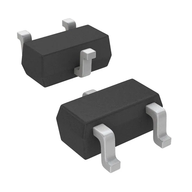
SC-75A (SOT-416)
G 1
3
D
Marking Code: E
S
2
ABSOLUTE MAXIMUM RATINGS (TA = 25_C UNLESS OTHERWISE NOTED)
Parameter
Drain-Source Voltage Gate-Source Voltage Continuous Drain Currenta Pulsed Drain Currenta TA = 25_C TA = 85_C TA = 25_C TA = 85_C
Symbol
VDS VGS ID IDM PD RthJA TJ, Tstg
Limit
60 "20 330 240 650 250 130 500 –55 to 150
Unit
V
mA
Power Dissipationa Thermal Resistance, Maximum Junction-to-Ambienta Operating Junction and Storage Temperature Range
mW _C/W _C
Notes c. Surface Mounted on FR4 Board, Power Applied for tv10 sec. Document Number: 71331 S-03049—Rev. A, 05-Feb-01 www.vishay.com
1
�Si1022R
Vishay Siliconix
New Product
SPECIFICATIONS (TJ = 25_C UNLESS OTHERWISE NOTED)
Limits Parameter Static
Drain-Source Breakdown Voltage Gate-Threshold Voltage V(BR)DSS VGS(th) VGS = 0 V, ID = 10 mA VDS = VGS, ID = 0.25 mA VDS = 0 V, VGS = "10 V Gate-Body Leakage IGSS TJ = 85_C VDS = 0 V, VGS = "5 V VDS = 50 V, VGS = 0 V Zero Gate Voltage Drain Current IDSS TJ = 85_C VDS = 60 V, VGS = 0 V On-State Drain Currenta VDS = 10 V, VGS = 4.5 V ID(on) VDS = 7.5 V, VGS = 10 V VGS = 4.5 V, ID = 200 mA Drain-Source On-Resistancea TJ = 125_C rDS(on) VGS = 10 V, ID = 500 mA TJ = 125_C Forward Transconductancea Diode Forward Voltagea gfs VSD VDS = 10 V, ID = 200 mA VGS = 0 V, IS = 200 mA 100 1.30 500 800 3.0 5.0 1.25 2.25 mS V W mA 60 1 2.5 "150 "500 "20 10 100 1 mA nA V
Symbol
Test Conditions
Min
Typ
Max
Unit
Dynamicb
Input Capacitance Output Capacitance Reverse Transfer Capacitance Gate Charge Ciss Coss Crss Qg VDS =10 V, ID = 250 mA VGS = 4.5 V VDS = 25 V, VGS = 0 V f = 1 MHz 30 6 2.5 0.6 nC pF
Switchingb, c
Turn-On Time Turn-Off Time t(on) t(off) VDD = 30 V, RL = 150 W ID = 200 mA, VGEN = 10 V RG = 10 W 25 ns 35 TNJO60
Notes a. Pulse test: PW v300 ms duty cycle v2%. b. For DESIGN AID ONLY, not subject to production testing. c. Switching time is essentially independent of operating temperature.
www.vishay.com
2
Document Number: 71331 S-03049—Rev. A, 05-Feb-01
�Si1022R
New Product
TYPICAL CHARACTERISTICS (25_C UNLESS NOTED)
Output Characteristics
1.0 6V VGS = 10 thru 7 V 0.8 I D – Drain Current (A) 5V I D – Drain Current (mA) 900 25_C 125_C 1200 TJ = –55_C
Vishay Siliconix
Transfer Characteristics
0.6 4V 0.4
600
300
0.2 3V 0.0 0 1 2 3 4 5 0 0 1 2 3 4 5 6
VDS – Drain-to-Source Voltage (V)
VGS – Gate-to-Source Voltage (V)
On-Resistance vs. Drain Current
4.0 3.5 r DS(on) – On-Resistance ( W )
50 VGS = 0 V f = 1 MHz 40
Capacitance
3.0 2.5 2.0 1.5 1.0 0.5 0.0 0 200 400 600 800 1000 0 0 5 10 15 20 25 VGS = 4.5 V VGS = 10 V C – Capacitance (pF) 30 Ciss 20 Coss 10 Crss
ID – Drain Current (mA)
VDS – Drain-to-Source Voltage (V)
Gate Charge
7 V GS – Gate-to-Source Voltage (V) 6 5 4 3 2 1 0 0.0 0.0 –50 VDS = 10 V ID = 250 mA 2.0
On-Resistance vs. Junction Temperature
VGS = 10 V @ 500 mA r DS(on) – On-Resistance ( W ) (Normalized) 1.6
1.2
VGS = 4.5 V @ 200 mA
0.8
0.4
0.1
0.2
0.3
0.4
0.5
0.6
–25
0
25
50
75
100
125
150
Qg – Total Gate Charge (nC)
TJ – Junction Temperature (_C)
Document Number: 71331 S-03049—Rev. A, 05-Feb-01
www.vishay.com
3
�Si1022R
Vishay Siliconix
New Product
TYPICAL CHARACTERISTICS (25_C UNLESS NOTED)
Source-Drain Diode Forward Voltage
1000 VGS = 0 V 4 100 TJ = 125_C r DS(on) – On-Resistance ( W ) I S – Source Current (A) 5
On-Resistance vs. Gate-Source Voltage
3
2 ID = 200 mA
ID = 500 mA
10
TJ = 25_C TJ = –55_C
1
1 0.00 0.3 0.6 0.9 1.2 1.5
0 0 2 4 6 8 10
VSD – Source-to-Drain Voltage (V)
VGS – Gate-to-Source Voltage (V)
Threshold Voltage Variance Over Temperature
0.4 3 2.5 ID = 250 mA –0.0 Power (W) 2
Single Pulse Power, Junction-to-Ambient
0.2 V GS(th) Variance (V)
–0.2
1.5
–0.4
1
TA = 25_C
–0.6
0.5
–0.8 –50
0 –25 0 25 50 75 100 125 150 0.01 0.1 1 Time (sec) 10 100 600 TJ – Junction Temperature (_C)
Normalized Thermal Transient Impedance, Junction-to-Ambient
2 Normalized Effective Transient Thermal Impedance 1 Duty Cycle = 0.5
0.2
Notes:
0.1 0.1 0.05
t1 PDM
0.02
t2 1. Duty Cycle, D =
2. Per Unit Base = RthJA = 500_C/W
t1 t2
Single Pulse 0.01 10–4 10–3 10–2 10–1 1 Square Wave Pulse Duration (sec)
3. TJM – TA = PDMZthJA(t) 4. Surface Mounted
10
100
600
www.vishay.com
4
Document Number: 71331 S-03049—Rev. A, 05-Feb-01
�
很抱歉,暂时无法提供与“SI1022R”相匹配的价格&库存,您可以联系我们找货
免费人工找货- 国内价格
- 1+1.97868
- 10+1.7988
- 30+1.67888
- 100+1.499
- 500+1.41506
- 1000+1.3551


 工商网监
湘ICP备2023018690号
工商网监
湘ICP备2023018690号
