PJM3401PSA
P-Enhancement Field Effect Transistor
Features
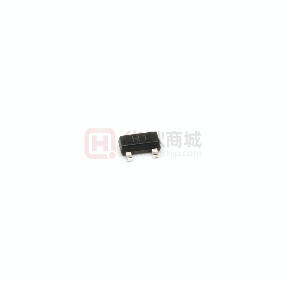
SOT-23
High density cell design for ultra low RDS(ON)
Fully characterized avalanche voltage and current
Excellent package for good heat dissipation
1. Gate
2.Source
3.Drain
Marking: R1
Applications
Schematic Diagram
Power switching application
Hard switched and high frequency circuits
Uninterruptible power supply
Drain
3
1
Gate
2 Source
Absolute Maximum Ratings
Ratings at TA =25℃ unless otherwise specified.
Parameter
Value
30
Units
Drain-Source Voltage
Symbol
-VDS
Gate-Source Voltage
VGS
±12
V
Continuous Drain Current
-ID
4.1
A
Power Dissipation
PD
1.2
W
TJ, TSTG
150, -55 to 150
°C
Symbol
Typ.
Units
RθJA
104
°C/W
Junction and Storage Temperature Range
V
Thermal Characteristics
Parameter
Maximum Junction-to-Ambient
www.pingjingsemi.com
Revision:2.0 Aug-2018
1/6
�PJM3401PSA
P-Enhancement Field Effect Transistor
Electrical Characteristics (TA=25℃ unless otherwise specified)
Symbol
Test Condition
Min.
Typ.
Max.
Units
Drain-source breakdown voltage
-V(BR)DSS
VGS = 0V, ID=-250µA
30
--
--
V
Drain to Source Leakage Current
-IDSS
VDS =-24V,VGS = 0V
--
--
1
µA
Gate-body leakage current
IGSS
VGS =±12V, VDS = 0V
--
--
±100
nA
Gate threshold voltage Note1
-VGS(th)
0.7
--
1.3
V
Drain-source on-resistance Note1
RDS(on)
VGS =-10V, ID =-4.1A
--
--
65
mΩ
VGS =-4.5V, ID =-2A
--
--
85
mΩ
Forward transconductance Note1
gFS
VDS =-5V, ID =-5A
7
--
--
S
--
954
--
--
115
--
Parameter
Static Characteristics
VDS =VGS, ID =-250µA
Dynamic characteristics
Input Capacitance
Ciss
Output Capacitance
Coss
Reverse Transfer Capacitance
Crss
--
77
--
td(on)
--
--
6.3
--
--
3.2
--
--
38.2
--
--
12
--
--
1
VDS = -15V,VGS = 0V,f=1MHz
pF
Switching Characteristics
Turn-on delay time
Turn-on rise time
Turn-off delay time
Turn-off fall time
tr
td(off)
VDD=-15V,
VGS=-10V,RGEN =6Ω,
RL =3.6Ω,
tf
ns
Source-Drain Diode characteristics
Diode Forward voltage
-VDS
VGS =0V, IS=-1A
V
Notes: 1. Pulse test ; pulse width ≤300μs, duty cycle ≤2%.
www.pingjingsemi.com
Revision:2.0 Aug-2018
2/6
�PJM3401PSA
P-Enhancement Field Effect Transistor
Typical Curves
Output Characteristics
-25
Ta=25℃
Ta=25℃
VGS=-10V
Pulsed
Pulsed
VGS=-4.5V
-4
(A)
VGS=-3.0V
-15
-3
-10
Drain Current
ID
ID
(A)
-20
Drain Current
Transfer Characteristics
-5
VGS=-2.5V
-2
-1
-5
VGS=-2.0V
-0
-1
-0
-2
-3
Drain to Source Voltage VDS
RDS(ON) ——
180
-4
-0
-0.5
-5
(V)
-1.0
-1.5
-2.0
Gate to Source Voltage
ID
RDS(ON) ——
180
VGS
-2.5
VGS
Ta=25℃
Ta=25℃
Pulsed
Pulsed
(mΩ)
150
VGS=-2.5V
RDS(ON)
120
90
On-Resistance
On-Resistance
RDS(ON)
(mΩ)
150
VGS=-4.5V
60
VGS=-10V
30
0
-3.0
(V)
120
90
ID=-2A
60
30
-0
-4
-2
Drain Current
IS
-10
-6
ID
——
0
-8
-0
-2
-4
-6
Gate to Source Voltage
(A)
VGS
-8
(V)
-10
Threshold Voltage
VSD
-1.2
Ta=25℃
Pulsed
-1
(V)
ID=-250uA
VTH
-0.01
Threshold Voltage
Source Current
IS
(A)
-1.0
-0.1
-1E-3
-0.8
-0.6
-1E-4
-1E-5
-0.0
-0.2
-0.4
-0.6
-0.8
Source to Drain Voltage VSD
www.pingjingsemi.com
Revision:2.0 Aug-2018
-1.0
(V)
-1.2
-0.4
25
50
75
Junction Temperature
100
Tj
125
(℃)
3/6
�PJM3401PSA
P-Enhancement Field Effect Transistor
Package Outline
SOT-23(TO-236)
0.8
Max.
1.025
1.150
A1
0.000
0.050
0.100
b
c
D
0.300
0.080
2.800
0.400
0.115
2.900
0.500
0.150
3.000
E
1.200
1.300
1.400
HE
2.250
2.400
2.550
e
1.800
1.900
2.000
0.300
0o
θ
0.8
1.9
SOT-23 (TO-236)
0.550REF
L1
L
2.2
Typ.
0.900
1.0
Min.
A
1.0
Dimensions in millimeter
Symbol
0.500
8o
Recommended Soldering Pad
Ordering Information
Device
PJM3401PSA
www.pingjingsemi.com
Revision:2.0 Aug-2018
Package
SOT-23
Shipping
3000/Reel&Tape(7inch)
4/6
�PJM3401PSA
P-Enhancement Field Effect Transistor
Conditions of Soldering and Storage
Recommended condition of reflow soldering
Recommended peak temperature is over 245 OC. If peak temperature is below 245 OC, you may adjust
the following parameters:
Time length of peak temperature (longer)
Time length of soldering (longer)
Thickness of solder paste (thicker)
Conditions of hand soldering
Temperature: 370 OC
Time: 3s max.
Times: one time
Storage conditions
Temperature
5 to 40 OC
Humidity
30 to 80% RH
Recommended period
One year after manufacturing
www.pingjingsemi.com
Revision:2.0 Aug-2018
5/6
�PJM3401PSA
P-Enhancement Field Effect Transistor
Package Specifications
1.The method of packaging and dimension are shown as below figure. (Units:mm)
Cover Tape
SOT-23 (TO-236)
3,000 pcs per reel
1
3
2
Carrier Tape
30,000 pcs per box
10 reels per box
240
217
0
455
21
43
5
120,000 pcs per carton
4 boxes per carton
220
2.. Tape and reel data (Units:mm)
D
A
T2
T1
4.0
4.0
B
8.0
C
E
1Pin
G
N
Tape (8mm)
F
Reel (7'')
www.pingjingsemi.com
Revision:2.0 Aug-2018
Symbol
A
B
C
E
F
D
T1
T2
N
G
Value (unit: mm)
Ø 177.8±1
2.7±0.2
Ø 13.5±0.2
Ø 54.5±0.2
12.3±0.3
9.6+2/-0.3
1.0±0.2
1.2±0.2
3.15±0.1
1.25±0.1
6/6
�
很抱歉,暂时无法提供与“PJM3401PSA”相匹配的价格&库存,您可以联系我们找货
免费人工找货- 国内价格
- 5+0.23800
- 20+0.21700
- 100+0.19600
- 500+0.17500
- 1000+0.16520
- 2000+0.15820


 工商网监
湘ICP备2023018690号
工商网监
湘ICP备2023018690号
