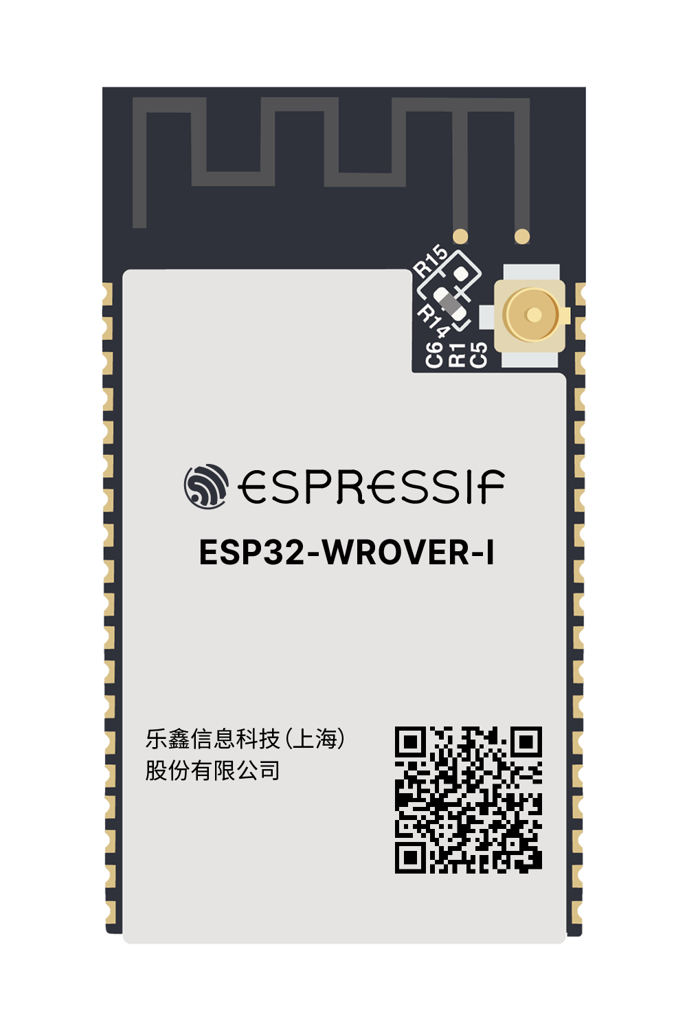
ESP32-WROVER
Datasheet
Version 2.0
Espressif Systems
Copyright © 2018
www.espressif.com
�About This Document
This document provides the specifications for the ESP32-WROVER modules with a PCB antenna or an IPEX
antenna.
Revision History
For revision history of this document, please refer to the last page.
Documentation Change Notification
Espressif provides email notifications to keep customers updated on changes to technical documentation. Please
subscribe at www.espressif.com/en/subscribe.
Certification
Download certificates for Espressif products from www.espressif.com/en/certificates.
Disclaimer and Copyright Notice
Information in this document, including URL references, is subject to change without notice. THIS DOCUMENT IS
PROVIDED AS IS WITH NO WARRANTIES WHATSOEVER, INCLUDING ANY WARRANTY OF MERCHANTABILITY, NON-INFRINGEMENT, FITNESS FOR ANY PARTICULAR PURPOSE, OR ANY WARRANTY OTHERWISE
ARISING OUT OF ANY PROPOSAL, SPECIFICATION OR SAMPLE.
All liability, including liability for infringement of any proprietary rights, relating to use of information in this document is disclaimed. No licenses express or implied, by estoppel or otherwise, to any intellectual property rights
are granted herein. The Wi-Fi Alliance Member logo is a trademark of the Wi-Fi Alliance. The Bluetooth logo is a
registered trademark of Bluetooth SIG.
All trade names, trademarks and registered trademarks mentioned in this document are property of their respective
owners, and are hereby acknowledged.
Copyright © 2018 Espressif Inc. All rights reserved.
�Contents
1 Overview
1
2 Pin Definitions
3
2.1
Pin Layout
3
2.2
Pin Description
4
2.3
Strapping Pins
5
3 Functional Description
7
3.1
CPU and Internal Memory
7
3.2
External Flash and SRAM
7
3.3
Crystal Oscillators
7
3.4
RTC and Low-Power Management
8
4 Peripherals and Sensors
9
5 Electrical Characteristics
10
5.1
Absolute Maximum Ratings
10
5.2
Recommended Operating Conditions
10
5.3
DC Characteristics (3.3 V, 25 °C)
10
5.4
Wi-Fi Radio
11
5.5
BLE Radio
11
5.6
5.5.1 Receiver
11
5.5.2 Transmitter
12
Reflow Profile
13
6 Schematics
14
7 Peripheral Schematics
15
8 Physical Dimensions
17
9 Recommended PCB Land Pattern
18
10U.FL Connector Dimensions
19
11Learning Resources
20
11.1 Must-Read Documents
20
11.2 Must-Have Resources
20
Revision History
21
�List of Tables
1
ESP32-WROVER Ordering Information
1
2
ESP32-WROVER Specifications
1
3
Pin Definitions
4
4
Strapping Pins
5
5
Absolute Maximum Ratings
10
6
Recommended Operating Conditions
10
7
DC Characteristics (3.3 V, 25 °C)
10
8
Wi-Fi Radio Characteristics
11
9
Receiver Characteristics – BLE
12
10
Transmitter Characteristics – BLE
12
�List of Figures
1
Pin Layout of ESP32-WROVER (Top View)
3
2
Reflow Profile
13
3
Schematics of ESP32-WROVER
14
4
Peripheral Schematics of ESP32-WROVER
15
5
Discharge Circuit for VDD33 Rail
15
6
Reset Circuit
16
7
Physical Dimensions of ESP32-WROVER
17
8
Recommended PCB Land Pattern of ESP32-WROVER
18
9
U.FL Connector Dimensions
19
�1. Overview
1. Overview
ESP32-WROVER is a powerful, generic WiFi-BT-BLE MCU module that targets a wide variety of applications,
ranging from low-power sensor networks to the most demanding tasks, such as voice encoding, music streaming
and MP3 decoding.
This module is provided in two versions: one with a PCB antenna, the other with an IPEX antenna. ESP32WROVER features a 4 MB external SPI flash and an additional 8 MB SPI Pseudo static RAM (PSRAM).
The ordering information on the two variants of ESP32-WROVER is listed as follows:
Table 1: ESP32-WROVER Ordering Information
Module
ESP32-WROVER (PCB)
ESP32-WROVER (IPEX)
Chip embedded
Flash
PSRAM
Dimensions (mm)
ESP32-D0WDQ6
4 MB
8 MB
(18.00±0.10)x(31.40±0.10)x(3.30±0.10)
For detailed ordering information, please see Espressif Product Ordering Information. For dimensions of the IPEX
connector, please see Chapter 10. The information in this datasheet is applicable to both modules.
At the core of this module is the ESP32-D0WDQ6 chip*. The chip embedded is designed to be scalable and
adaptive. There are two CPU cores that can be individually controlled, and the CPU clock frequency is adjustable
from 80 MHz to 240 MHz. The user may also power off the CPU and make use of the low-power co-processor to
constantly monitor the peripherals for changes or crossing of thresholds. ESP32 integrates a rich set of peripherals,
ranging from capacitive touch sensors, Hall sensors, SD card interface, Ethernet, high-speed SPI, UART, I²S and
I²C.
Note:
* For details on the part numbers of the ESP32 family of chips, please refer to the document ESP32 Datasheet.
The integration of Bluetooth, Bluetooth LE and Wi-Fi ensures that a wide range of applications can be targeted,
and that the module is all-around: using Wi-Fi allows a large physical range and direct connection to the Internet
through a Wi-Fi router, while using Bluetooth allows the user to conveniently connect to the phone or broadcast
low energy beacons for its detection. The sleep current of the ESP32 chip is less than 5 µA, making it suitable
for battery powered and wearable electronics applications. The module supports a data rate of up to 150 Mbps,
and 20 dBm output power at the antenna to ensure the widest physical range. As such the module does offer
industry-leading specifications and the best performance for electronic integration, range, power consumption,
and connectivity.
The operating system chosen for ESP32 is freeRTOS with LwIP; TLS 1.2 with hardware acceleration is built in as
well. Secure (encrypted) over the air (OTA) upgrade is also supported, so that users can upgrade their products
even after their release, at minimum cost and effort.
Table 2 provides the specifications of ESP32-WROVER.
Table 2: ESP32-WROVER Specifications
Categories
Items
Specifications
Certification
RF certification
FCC/CE-RED/SRRC/TELEC
Wi-Fi certification
Wi-Fi Alliance
Espressif Systems
1
ESP32-WROVER Datasheet V2.0
�1. Overview
Categories
Test
Items
Specifications
Bluetooth certification
BQB
Green certification
RoHS/REACH
Reliablity
HTOL/HTSL/uHAST/TCT/ESD
802.11 b/g/n (802.11n up to 150 Mbps)
Wi-Fi
Protocols
A-MPDU and A-MSDU aggregation and 0.4 µs guard interval support
Frequency range
2.4 GHz ~ 2.5 GHz
Protocols
Bluetooth v4.2 BR/EDR and BLE specification
NZIF receiver with –97 dBm sensitivity
Bluetooth
Radio
Class-1, class-2 and class-3 transmitter
AFH
Audio
CVSD and SBC
SD card, UART, SPI, SDIO, I2 C, LED PWM, Motor PWM,
Module interfaces
I2 S, IR, pulse counter, GPIO, capacitive touch sensor,
ADC, DAC
Hardware
On-chip sensor
Hall sensor
Integrated crystal
40 MHz crystal
Integrated SPI flash
4 MB
Integrated PSRAM
8 MB
Operating voltage/Power supply
2.3 V ~ 3.6 V
Operating current
Average: 80 mA
Minimum current delivered by
power supply
Recommended operating temperature range
Package size
Espressif Systems
500 mA
–40 °C ~ 85 °C
(18.00±0.10) mm x (31.40±0.10) mm x (3.30±0.10) mm
2
ESP32-WROVER Datasheet V2.0
�2. Pin Definitions
2. Pin Definitions
2.1 Pin Layout
Keepout Zone
1
GND
GND
38
2
VDD33
IO23
37
3
EN
IO22
36
4
SENSOR_VP
TXD0
35
5
SENSOR_VN
RXD0
34
6
IO34
IO21
33
7
IO35
NC
32
IO19
31
39 GND
8
IO32
9
IO33
IO18
30
10
IO25
IO5
29
11
IO26
NC
28
12
IO27
NC
27
13
IO14
IO4
26
14
IO12
IO0
25
15
GND
IO2
24
16
IO13
IO15
23
17
SD2
SD1
22
18
SD3
SD0
21
19
CMD
CLK
20
Figure 1: Pin Layout of ESP32-WROVER (Top View)
Espressif Systems
3
ESP32-WROVER Datasheet V2.0
�2. Pin Definitions
2.2 Pin Description
ESP32-WROVER has 38 pins. See pin definitions in Table 3.
Table 3: Pin Definitions
Name
No.
Type
Function
GND
1
P
Ground
3V3
2
P
Power supply
EN
3
I
Module-enable signal. Active high.
SENSOR_VP
4
I
GPIO36, ADC1_CH0, RTC_GPIO0
SENSOR_VN
5
I
GPIO39, ADC1_CH3, RTC_GPIO3
IO34
6
I
GPIO34, ADC1_CH6, RTC_GPIO4
IO35
7
I
GPIO35, ADC1_CH7, RTC_GPIO5
IO32
8
I/O
IO33
9
I/O
IO25
10
I/O
GPIO25, DAC_1, ADC2_CH8, RTC_GPIO6, EMAC_RXD0
IO26
11
I/O
GPIO26, DAC_2, ADC2_CH9, RTC_GPIO7, EMAC_RXD1
IO27
12
I/O
GPIO27, ADC2_CH7, TOUCH7, RTC_GPIO17, EMAC_RX_DV
IO14
13
I/O
IO12
14
I/O
GND
15
P
IO13
16
I/O
SHD/SD2*
17
I/O
GPIO9, SD_DATA2, SPIHD, HS1_DATA2, U1RXD
SWP/SD3*
18
I/O
GPIO10, SD_DATA3, SPIWP, HS1_DATA3, U1TXD
SCS/CMD*
19
I/O
GPIO11, SD_CMD, SPICS0, HS1_CMD, U1RTS
SCK/CLK*
20
I/O
GPIO6, SD_CLK, SPICLK, HS1_CLK, U1CTS
SDO/SD0*
21
I/O
GPIO7, SD_DATA0, SPIQ, HS1_DATA0, U2RTS
SDI/SD1*
22
I/O
GPIO8, SD_DATA1, SPID, HS1_DATA1, U2CTS
IO15
23
I/O
IO2
24
I/O
IO0
25
I/O
IO4
26
I/O
NC1
27
-
-
NC2
28
-
-
IO5
29
I/O
GPIO5, VSPICS0, HS1_DATA6, EMAC_RX_CLK
IO18
30
I/O
GPIO18, VSPICLK, HS1_DATA7
Espressif Systems
GPIO32, XTAL_32K_P (32.768 kHz crystal oscillator input), ADC1_CH4,
TOUCH9, RTC_GPIO9
GPIO33, XTAL_32K_N (32.768 kHz crystal oscillator output),
ADC1_CH5, TOUCH8, RTC_GPIO8
GPIO14, ADC2_CH6, TOUCH6, RTC_GPIO16, MTMS, HSPICLK,
HS2_CLK, SD_CLK, EMAC_TXD2
GPIO12, ADC2_CH5, TOUCH5, RTC_GPIO15, MTDI, HSPIQ,
HS2_DATA2, SD_DATA2, EMAC_TXD3
Ground
GPIO13, ADC2_CH4, TOUCH4, RTC_GPIO14, MTCK, HSPID,
HS2_DATA3, SD_DATA3, EMAC_RX_ER
GPIO15, ADC2_CH3, TOUCH3, MTDO, HSPICS0, RTC_GPIO13,
HS2_CMD, SD_CMD, EMAC_RXD3
GPIO2, ADC2_CH2, TOUCH2, RTC_GPIO12, HSPIWP, HS2_DATA0,
SD_DATA0
GPIO0, ADC2_CH1, TOUCH1, RTC_GPIO11, CLK_OUT1,
EMAC_TX_CLK
GPIO4, ADC2_CH0, TOUCH0, RTC_GPIO10, HSPIHD, HS2_DATA1,
SD_DATA1, EMAC_TX_ER
4
ESP32-WROVER Datasheet V2.0
�2. Pin Definitions
Name
No.
Type
Function
IO19
31
I/O
GPIO19, VSPIQ, U0CTS, EMAC_TXD0
NC
32
-
-
IO21
33
I/O
GPIO21, VSPIHD, EMAC_TX_EN
RXD0
34
I/O
GPIO3, U0RXD, CLK_OUT2
TXD0
35
I/O
GPIO1, U0TXD, CLK_OUT3, EMAC_RXD2
IO22
36
I/O
GPIO22, VSPIWP, U0RTS, EMAC_TXD1
IO23
37
I/O
GPIO23, VSPID, HS1_STROBE
GND
38
P
Ground
Notice:
* Pins SCK/CLK, SDO/SD0, SDI/SD1, SHD/SD2, SWP/SD3 and SCS/CMD, namely, GPIO6 to GPIO11 are connected
to the SPI flash integrated on the module and are not recommended for other uses.
2.3 Strapping Pins
ESP32 has five strapping pins, which can be seen in Chapter 6 Schematics:
• MTDI
• GPIO0
• GPIO2
• MTDO
• GPIO5
Software can read the values of these five bits from register ”GPIO_STRAPPING”.
During the chip’s system reset (power-on-reset, RTC watchdog reset and brownout reset), the latches of the
strapping pins sample the voltage level as strapping bits of ”0” or ”1”, and hold these bits until the chip is powered
down or shut down. The strapping bits configure the device’s boot mode, the operating voltage of VDD_SDIO and
other initial system settings.
Each strapping pin is connected to its internal pull-up/pull-down during the chip reset. Consequently, if a strapping
pin is unconnected or the connected external circuit is high-impedance, the internal weak pull-up/pull-down will
determine the default input level of the strapping pins.
To change the strapping bit values, users can apply the external pull-down/pull-up resistances, or use the host
MCU’s GPIOs to control the voltage level of these pins when powering on ESP32.
After reset, the strapping pins work as normal-function pins.
Refer to Table 4 for a detailed boot-mode configuration by strapping pins.
Table 4: Strapping Pins
Voltage of Internal LDO (VDD_SDIO)
Pin
Default
MTDI
Pull-down
Espressif Systems
3.3 V
1.8 V
0
1
5
ESP32-WROVER Datasheet V2.0
�2. Pin Definitions
Booting Mode
Pin
Default
SPI Boot
Download Boot
GPIO0
Pull-up
1
0
GPIO2
Pull-down
Don’t-care
0
Enabling/Disabling Debugging Log Print over U0TXD During Booting
Pin
Default
U0TXD Active
U0TXD Silent
MTDO
Pull-up
1
0
Timing of SDIO Slave
Pin
Default
MTDO
GPIO5
Falling-edge
Input
Falling-edge
Input
Rising-edge
Input
Rising-edge
Input
Falling-edge Output
Rising-edge Output
Falling-edge Output
Rising-edge Output
Pull-up
0
0
1
1
Pull-up
0
1
0
1
Note:
• Firmware can configure register bits to change the settings of ”Voltage of Internal LDO (VDD_SDIO)” and ”Timing
of SDIO Slave” after booting.
• The MTDI is internally pulled high in the module, as the flash and SRAM in ESP32-WROVER only support a power
voltage of 1.8 V (output by VDD_SDIO).
Espressif Systems
6
ESP32-WROVER Datasheet V2.0
�3. Functional Description
3. Functional Description
This chapter describes the modules and functions integrated in ESP32-WROVER.
3.1 CPU and Internal Memory
ESP32-D0WDQ6 contains two low-power Xtensa® 32-bit LX6 microprocessors. The internal memory includes:
• 448 KB of ROM for booting and core functions.
• 520 KB of on-chip SRAM for data and instructions.
• 8 KB of SRAM in RTC, which is called RTC FAST Memory and can be used for data storage; it is accessed
by the main CPU during RTC Boot from the Deep-sleep mode.
• 8 KB of SRAM in RTC, which is called RTC SLOW Memory and can be accessed by the co-processor during
the Deep-sleep mode.
• 1 Kbit of eFuse: 256 bits are used for the system (MAC address and chip configuration) and the remaining
768 bits are reserved for customer applications, including flash-encryption and chip-ID.
3.2 External Flash and SRAM
ESP32 supports multiple external QSPI flash and SRAM chips. More details can be found in Chapter SPI in the
ESP32 Technical Reference Manual. ESP32 also supports hardware encryption/decryption based on AES to protect developers’ programs and data in flash.
ESP32 can access the external QSPI flash and SRAM through high-speed caches.
• The external flash can be mapped into CPU instruction memory space and read-only memory space simultaneously.
– When external flash is mapped into CPU instruction memory space, up to 11 MB + 248 KB can be
mapped at a time. Note that if more than 3 MB + 248 KB are mapped, cache performance will be
reduced due to speculative reads by the CPU.
– When external flash is mapped into read-only data memory space, up to 4 MB can be mapped at a
time. 8-bit, 16-bit and 32-bit reads are supported.
• External SRAM can be mapped into CPU data memory space. Up to 4 MB can be mapped at a time. 8-bit,
16-bit and 32-bit reads and writes are supported.
ESP32-WROVER integrates a 4 MB of external SPI flash and an 8 MB PSRAM for more memory space.
3.3 Crystal Oscillators
The module uses a 40-MHz crystal oscillator.
Espressif Systems
7
ESP32-WROVER Datasheet V2.0
�3. Functional Description
3.4 RTC and Low-Power Management
With the use of advanced power-management technologies, ESP32 can switch between different power modes.
For details on ESP32’s power consumption in different power modes, please refer to section ”RTC and Low-Power
Management” in ESP32 Datasheet.
Espressif Systems
8
ESP32-WROVER Datasheet V2.0
�4. Peripherals and Sensors
4. Peripherals and Sensors
Please refer to Section Peripherals and Sensors in ESP32 Datasheet.
Note:
External connections can be made to any GPIO except for GPIOs in the range 6-11, 16, or 17. GPIOs 6-11 are connected
to the module’s integrated SPI flash and PSRAM. GPIOs 16 and 17 are connected to the module’s integrated PSRAM.
For details, please see Chapter 6 Schematics.
Espressif Systems
9
ESP32-WROVER Datasheet V2.0
�5. Electrical Characteristics
5. Electrical Characteristics
5.1 Absolute Maximum Ratings
Stresses beyond the absolute maximum ratings listed in the table below may cause permanent damage to the
device. These are stress ratings only, and do not refer to the functional operation of the device that should follow
the recommended operating conditions.
Table 5: Absolute Maximum Ratings
Symbol
Parameter
Min
Max
Unit
VDD33
Power supply voltage
–0.3
3.6
V
Cumulative IO output current
-
1,100
mA
Storage temperature
–40
150
°C
Ioutput
1
Tstore
1. The module worked properly after a 24-hour test in ambient temperature at 25 °C, and the IOs in three domains
(VDD3P3_RTC, VDD3P3_CPU, VDD_SDIO) output high logic level to ground. Please note that pins occupied by flash
and/or PSRAM in the VDD_SDIO power domain were excluded from the test.
2. Please see Appendix IO_MUX of ESP32 Datasheet for IO’s power domain.
5.2 Recommended Operating Conditions
Table 6: Recommended Operating Conditions
Symbol
Parameter
Min
Typical
Max
Unit
VDD33
-
2.3
3.3
3.6
V
IV DD
Current delivered by external power supply
0.5
-
-
A
T
Operating temperature
–40
-
85
°C
5.3 DC Characteristics (3.3 V, 25 °C)
Table 7: DC Characteristics (3.3 V, 25 °C)
Symbol
CIN
VIH
Parameter
Min
Pin capacitance
-
High-level input voltage
0.75×VDD
1
Typ
Max
2
-
-
Unit
pF
1
VDD +0.3
V
1
VIL
Low-level input voltage
–0.3
-
0.25×VDD
IIH
High-level input current
-
-
50
nA
IIL
Low-level input current
-
-
50
nA
-
-
VOH
VOL
High-level output voltage
0.8×VDD
Low-level output voltage
High-level source current
1
IOH
1
(VDD = 3.3 V, VOH >= 2.64 V,
output drive strength set to the
maximum)
Espressif Systems
V
V
1
-
-
0.1×VDD
V
VDD3P3_CPU power domain
1, 2
-
40
-
mA
VDD3P3_RTC power domain
1, 2
-
40
-
mA
-
20
-
mA
VDD_SDIO power domain 1,
10
3
ESP32-WROVER Datasheet V2.0
�5. Electrical Characteristics
Symbol
Parameter
Min
Typ
Max
Unit
-
28
-
mA
Low-level sink current
IOL
(VDD1 = 3.3 V, VOL = 0.495 V,
output drive strength set to the maximum)
RP U
Resistance of internal pull-up resistor
-
45
-
kΩ
RP D
Resistance of internal pull-down resistor
-
45
-
kΩ
VIL_nRST
Low-level input voltage of CHIP_PU to reset the chip
-
-
0.6
V
Notes:
1. Please see Appendix IO_MUX of ESP32 Datasheet for IO’s power domain. VDD is the I/O voltage for a particular power
domain of pins.
2. For VDD3P3_CPU and VDD3P3_RTC power domain, per-pin current sourced in the same domain is gradually reduced
from around 40 mA to around 29 mA, VOH >=2.64 V, as the number of current-source pins increases.
3. Pins occupied by flash and/or PSRAM in the VDD_SDIO power domain were excluded from the test.
5.4 Wi-Fi Radio
Table 8: Wi-Fi Radio Characteristics
Parameter
Condition
Min
Typical
Max
Unit
Input frequency
-
2412
-
2484
MHz
Output impedance*
-
-
*
-
Ω
TX power
11n, MCS7
12
13
14
dBm
11b mode
17.5
18.5
20
dBm
11b, 1 Mbps
-
–98
-
dBm
11b, 11 Mbps
-
–89
-
dBm
11g, 6 Mbps
-
–92
-
dBm
11g, 54 Mbps
-
–74
-
dBm
11n, HT20, MCS0
-
–91
-
dBm
11n, HT20, MCS7
-
–71
-
dBm
11n, HT40, MCS0
-
–89
-
dBm
11n, HT40, MCS7
-
–69
-
dBm
11g, 6 Mbps
-
31
-
dB
11g, 54 Mbps
-
14
-
dB
11n, HT20, MCS0
-
31
-
dB
11n, HT20, MCS7
-
13
-
dB
Sensitivity
Adjacent channel rejection
∗
For the modules that use IPEX antennas, the output impedance is 50 Ω. For other modules without IPEX antennas, users do
not need to concern about the output impedance.
5.5 BLE Radio
5.5.1 Receiver
Espressif Systems
11
ESP32-WROVER Datasheet V2.0
�5. Electrical Characteristics
Table 9: Receiver Characteristics – BLE
Parameter
Conditions
Min
Typ
Max
Unit
Sensitivity @30.8% PER
-
-
–97
-
dBm
Maximum received signal @30.8% PER
-
0
-
-
dBm
Co-channel C/I
-
-
+10
-
dB
F = F0 + 1 MHz
-
–5
-
dB
F = F0 – 1 MHz
-
–5
-
dB
F = F0 + 2 MHz
-
–25
-
dB
F = F0 – 2 MHz
-
–35
-
dB
F = F0 + 3 MHz
-
–25
-
dB
F = F0 – 3 MHz
-
–45
-
dB
30 MHz ~ 2000 MHz
–10
-
-
dBm
2000 MHz ~ 2400 MHz
–27
-
-
dBm
2500 MHz ~ 3000 MHz
–27
-
-
dBm
3000 MHz ~ 12.5 GHz
–10
-
-
dBm
-
–36
-
-
dBm
Adjacent channel selectivity C/I
Out-of-band blocking performance
Intermodulation
5.5.2 Transmitter
Table 10: Transmitter Characteristics – BLE
Parameter
Conditions
Min
Typ
Max
Unit
RF transmit power
-
-
0
-
dBm
Gain control step
-
-
3
-
dBm
RF power control range
-
–12
-
+12
dBm
F = F0 ± 2 MHz
-
–52
-
dBm
F = F0 ± 3 MHz
-
–58
-
dBm
F = F0 ± > 3 MHz
-
–60
-
dBm
∆ f 1avg
-
-
-
265
kHz
∆ f 2max
-
247
-
-
kHz
∆ f 2avg /∆ f 1avg
-
-
–0.92
-
-
ICFT
-
-
–10
-
kHz
Drift rate
-
-
0.7
-
kHz/50 µs
Drift
-
-
2
-
kHz
Adjacent channel transmit power
Espressif Systems
12
ESP32-WROVER Datasheet V2.0
�5. Electrical Characteristics
Temperature (℃)
5.6 Reflow Profile
Peak Temp.
235 ~ 250℃
250
Preheating zone
150 ~ 200℃
60 ~ 120s
217
200
Reflow zone
!217℃ 60 ~ 90s
Cooling zone
-1 ~ -5℃/s
Soldering time
> 30s
Ramp-up zone
1 ~ 3℃/s
100
50
25
Time (sec.)
0
0
50
100
150
200
250
Ramp-up zone — Temp.: 217℃ 7LPH��60 ~ 90s; Peak Temp.: 235 ~ 250℃ (


 工商网监
湘ICP备2023018690号
工商网监
湘ICP备2023018690号