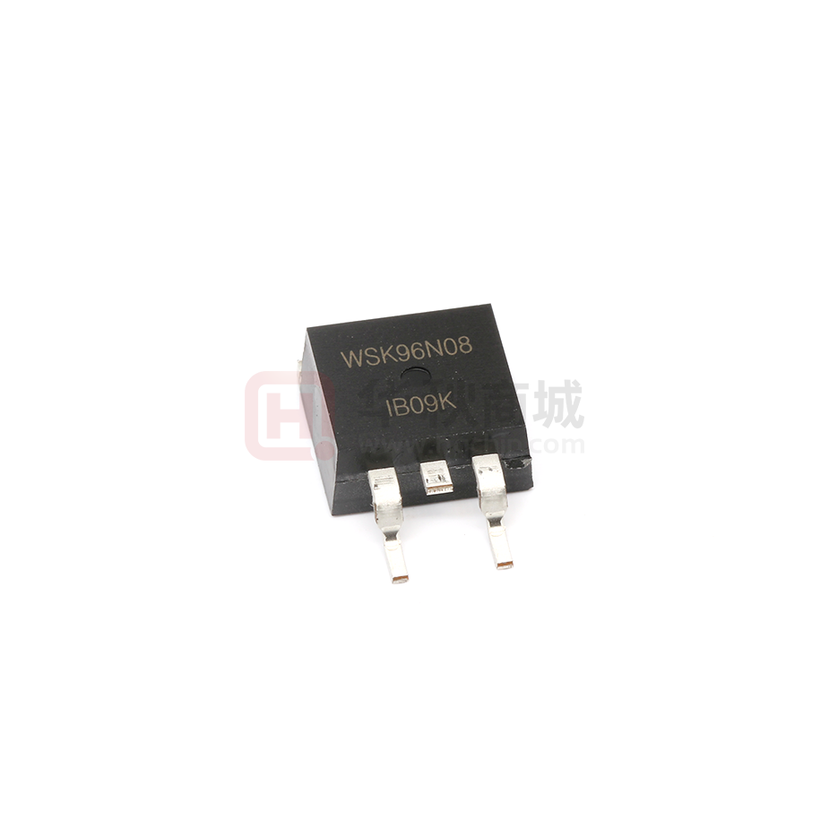
WSK96N08
N-Ch MOSFET
Product Summery
General Description
BVDSS
The WSK96N08 is the highest performance
trench N-ch MOSFET with extreme high cell
density , which provide excellent RDSON
and gate charge for most of the synchronous
buck converter applications .
80V
The WSK96N08 meet the RoHS and Green
Product requirement , 100% EAS
guaranteed with full function reliability
approved.
RDSON
ID
7mΩ
96A
TO-263-2L Pin Configuration
Applications
z Switching application
z Power management for inverter systems
Absolute Maximum Ratings
Symbol
Parameter
Rating
Units
VDS
Drain-Source Voltage
80
V
VGS
Gate-Source Voltage
±25
V
1
90
A
1
64
A
360**
A
416***
mJ
ID@TC=25℃
ID@TC=100℃
IDM
EAS
Continuous Drain Current, VGS @ 10V
Continuous Drain Current, VGS @ 10V
Pulsed Drain Current
2
3
Single Pulse Avalanche Energy
IAS
Avalanche Current
200
PD@TC=25℃
Total Power Dissipation3
185
W
PD@TC=100℃
Total Power Dissipation3
92
W
TSTG
Storage Temperature Range
-55 to 175
℃
TJ
Operating Junction Temperature Range
-55 to 175
℃
Note:
A
* Repetitive rating;pulse width limited by max.junction temperature.
** Surface mounted on 1in2 FR-4 board.
*** Limited by TJmax , starting TJ=25°C , L = 0.5mH, RG= 25Ω, VGS =10V.
www.winsok.tw
Page 1
Dec.2014
�WSK96N08
N-Ch MOSFET
Electrical Characteristics (TJ=25 ℃, unless otherwise noted)
Symbol
BVDSS
Parameter
Drain-Source Breakdown Voltage
△BVDSS/△TJ BVDSS Temperature Coefficient
RDS(ON)
Static Drain-Source On-Resistance2
VGS(th)
Gate Threshold Voltage
△VGS(th)
VGS(th) Temperature Coefficient
IDSS
Drain-Source Leakage Current
IGSS
Gate-Source Leakage Current
gf
gfs
orward Transconductance
V
V/℃
0.0
VGS=10V , ID=45A
---
7
9
mΩ
VGS=6V , ID=10A
---
10
12
mΩ
2
3
4
V
---
mV/℃
VGS=VDS , ID =250uA
---
-6.57
VDS=80V , VGS=0V , TJ=25℃
-----
-
1
VDS=80V , VGS=0V , TJ=55℃
---
-
2
VGS=±20V , VDS=0V
---
-
±100
nA
VDS=5V , ID=20A
18
---
---
S
---
Gate-Drain Charge
---
28
---
Turn-On Delay Time
---
25
---
VDS=50V , VGS=10V , ID=120A
uA
nC
Rise Time
VDD=30V , VGS=10V ,
---
42
---
Turn-Off Delay Time
RG=6Ω ID=145A ,
---
62
---
Fall Time
RL=30Ω
---
19
---
---
3800
---
---
389
---
---
250
---
---
0.8
---
V
---
60
---
ns
---
125
---
nC
Ciss
Input Capacitance
Coss
Output Capacitance
Crss
Reverse Transfer Capacitance
VSD
Diode Forward Voltage
trr
Reverse Recovery Time
Qrr
-----
---
16
Qgd
Unit
Reference to 25℃ , ID=1mA
86
Gate-Source Charge
Tf
---
Max.
---
Total Gate Charge (10V)
Td(off)
80
Typ.
---
Qg
Tr
VGS=0V , ID=250uA
Min.
---
Qgs
Td(on)
Conditions
VDS=30V , VGS=0V , f=1MHz
Reverse Recovery Charge
ISD=45A,VGS=0V
ISD=45A,dISD/dt=100A/μs
ns
pF
Note: *Pulse test,pulse width ≤ 300us,duty cycle ≤ 2%
www.winsok.tw
Page 2
Dec.2014
�WSK96N08
N-Ch MOSFET
Typical Operating Characteristics
Figure 2: Drain Current
ID-Drain Current(A)
Power Dissipation (w)
Figure 1: Power Dissipation
Tc-Case Temperature(℃)
Tc-Case Temperature(℃)
Thermal
Zθjc
ID-Drain Current(A)
Impedance
Figure 4: Thermal Transient Impedance
Normalized Transient
Figure 3: Safe Operation Area
Maximum Effective Transient Thermal
Impedance, Junction-to-Case
Figure 5: Output Characteristics
Figure 6: Drain-Source On Resistance
ID-Drain Current(A)
RDS(ON)-ON-Resistance(mΩ)
VDS-Drain-Source Voltage(V)
VDS-Drain-Source Voltage (V)
www.winsok.tw
ID-Drain Current(A)
Page 3
Dec.2014
�WSK96N08
N-Ch MOSFET
Typical Operating Characteristics
Figure 8: Source-Drain Diode Forward
IS-Source Current (A)
Normalized On-Resistance
Figure 7: On-Resistance vs. Temperature
Tj-Junction Temperature (℃)
Figure 9: Capacitance Characteristics
Figure 10: Gate Charge Characteristics
C-Capacitance(pF)
VGS-Gate-Source Voltage (V)
12
VSD-Source-Drain Voltage(V)
VDS-Drain-Source Voltage (V)
www.winsok.tw
Q G-Gate Charge (nC)
Page 4
Dec.2014
�WSK96N08
N-Ch MOSFET
Device Per Unit
Package Type
Unit
Quantity
TO-263-2L
Reel
50
Package Information
TO-263-2L
COMMON DIMENSIONS
SYMBOL
mm
MIN
NOM
MAX
A
4.37
4.57
4.77
A1
1.22
1.27
1.42
A2
2.49
2.69
2.89
A3
0
0.13
0.25
b
0.7
0.81
0.96
b1
1.17
1.27
1.47
c
0.3
0.38
0.53
D1
8.5
8.7
8.9
D4
6.6
-
-
E
9.86
10.16
10.36
E5
7.06
-
-
2.54 BSC
e
H
14.7
15.1
15.5
H2
1.07
1.27
1.47
L
2
2.3
2.6
L1
1.4
1.55
1.7
L4
θ
www.winsok.tw
0.25 BSC
0°
Page 5
5°
9°
Dec.2014
�WSK96N08
N-Ch MOSFET
Classification Profile
Classification Reflow Profiles
Profile Feature
Preheat & Soak
Temperature min (Tsmin)
Temperature max (Tsmax)
Time (Tsmin to Tsmax) (ts)
Average ramp-up rate
(Tsmaxto TP)
Liquidous temperature (TL)
Time at liquidous (tL)
Peak package body Temperature
(Tp)*
Time (tP)** within 5°C of the specified
classification temperature (Tc)
Average ramp-down rate (Tpto Tsmax)
Time 25°C to peak temperature
Sn-Pb Eutectic Assembly
Pb-Free Assembly
100 °C
150 °C
150 °C
200 °C
60-120 seconds
60-120 seconds
3 °C/second max.
3°C/second max.
183 °C
217 °C
60-150 seconds
60-150 seconds
See Classification Temp in table 1
SeeClassification Tempin table 2
20** seconds
30** seconds
6 °C/second max.
6 °C/second max.
6 minutes max.
8 minutes max.
*Tolerance for peak profile Temperature (T p) is defined as a supplier minimum and a user maximum.
** Tolerance for time at peak profile temperature (tp) is defined as a supplier minimum and a user maximum.
www.winsok.tw
Page 6
Dec.2014
�Attention�
1,�Any�and�all�Winsok�power�products�described�or�contained�herein�do�not�have�specifications�that�can�handle�
applications�that�require�extremely�high�levels�of�reliability,�such�as�lifeͲsupport�systems,�aircraft's�control�systems,�or�
other�applications�whose�failure�can�be�reasonably�expected�to�result�in�serious�physical�and/or�material�damage.� �
Consult�with�your�Winsok�power�representative�nearest�you�before�using�any�Winsok�power�products�described�or�
contained�herein�in�such�applications.�
2,Winsok�power�assumes�no�responsibility�for�equipment�failures�that�result�from�using�products�at�values�that�exceed,� �
even�momentarily,�rated�values�(such�as�maximum�ratings,�operating�condition�ranges,�or�other�parameters)�listed�in�
products�specifications�of�any�and�all�Winsok�power�products�described�or�contained�herein.�
3,�Specifications�of�any�and�all�Winsok�power�products�described�or�contained�herein�stipulate�the�performance,�
characteristics,�and�functions�of�the�described�products�in�the�independent�state,�and�are�not�guarantees�of�the�
performance,�characteristics,�and�functions�of�the�described�products�as�mounted�in�the�customer’s�products�or�
equipment.�To�verify�symptoms�and�states�that�cannot�be�evaluated�in�an�independent�device,�the�customer�should�always�
evaluate�and�test�devices�mounted�in�the�customer’s�products�or�equipment.�
4,�Winsok�power�Semiconductor�CO.,�LTD.�strives�to�supply�highͲquality�highͲreliability�products.�However,�any�and�all�
semiconductor�products�fail�with�some�probability.�It�is�possible�that�these�probabilistic�failures�could�give�rise�to�accidents�
or�events�that�could�endanger�human�lives�that�could�give�rise�to�smoke�or�fire,�or�that�could�cause�damage�to�other�
property.�When�designing�equipment,�adopt�safety�measures�so�that�these�kinds�of�accidents�or�events�cannot�occur.�Such�
measures�include�but�are�not�limited�to�protective�circuits�and�error�prevention�circuits�for�safe�design,�redundant�design,�
and�structural�design.�
5,In�the�event�that�any�or�all�Winsok�power�products(including�technical�data,�services)�described�or�contained�herein�are�
controlled�under�any�of�applicable�local�export�control�laws�and�regulations,�such�products�must�not�be�exported�without�
obtaining�the�export�license�from�the�authorities�concerned�in�accordance�with�the�above�law.�
6,�No�part�of�this�publication�may�be�reproduced�or�transmitted�in�any�form�or�by�any�means,�electronic�or�mechanical,�
including�photocopying�and�recording,�or�any�information�storage�or�retrieval�system,�or�otherwise,�without�the�prior�
written�permission�of�Winsok�power�Semiconductor�CO.,�LTD.�
7,�Information�(including�circuit�diagrams�and�circuit�parameters)�herein�is�for�example�only;�it�is�not�guaranteed�for�
volume�production. Winsok�power�believes�information�herein�is�accurate�and�reliable,�but�no�guarantees�are�made�or�
implied�regarding�its�use�or�any�infringements�of�intellectual�property�rights�or�other�rights�of�third�parties.�
8,�Any�and�all�information�described�or�contained�herein�are�subject�to�change�without�notice�due�to�product/technology�
improvement,etc.�When�designing�equipment,�refer�to�the�"Delivery�Specification"�for�the�Winsok�power�product�that�you� �
Intend�to�use.�
9,�this�catalog�provides�information�as�of�Sep.2014. Specifications�and�information�herein�are�subject�to�change�without�
notice.�
�


 工商网监
湘ICP备2023018690号
工商网监
湘ICP备2023018690号
