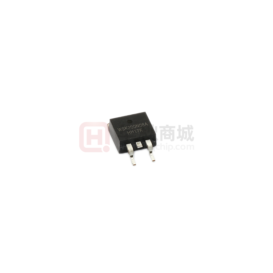
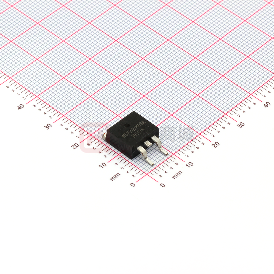
WSK200N08A
N-Ch MOSFET
General Description
Product Summery
The WSK200N08A is the highest performance
trench N-Ch MOSFET with extreme high cell
density , which provide excellent RDSON and
gate charge for most of the synchronous buck
converter applications .
The WSK200N08A meet the RoHS and Green
Product requirement,100% EAS guaranteed
with full function reliability approved.
BVDSS
RDSON
ID
80V
3mΩ
200A
Applications
High power DC/DC converters and switch mode
power supply
Features
DC Motor control and Class D Amplifier
z Advanced high cell density Trench technology
z Super Low Gate Charge
TO-263 Pin Configuration
z Excellent CdV/dt effect decline
z 100% EAS Guaranteed
z Green Device Available
Absolute Maximum Ratings
Symbol
Parameter
Rating
Units
VDS
Drain-Source Voltage
80
V
VGS
Gate-Source Voltage
±25
V
1
ID@TC=25℃
Continuous Drain Current, VGS @ 10V
200
A
ID@TC=100℃
Continuous Drain Current, VGS @ 10V1
144
A
790
A
IDM
2,
Pulsed Drain Current TC=25°C
EAS
Avalanche Energy, Single pulse,L=0.5mH
1496
mJ
IAS
Avalanche Current, Single pulse,L=0.5mH
PD@TC=25℃
200
A
4
345
W
4
Total Power Dissipation
PD@TC=100℃
Total Power Dissipation
173
W
TSTG
Storage Temperature Range
-55 to 175
℃
Operating Junction Temperature Range
175
℃
TJ
Thermal Data
Symbol
Parameter
RθJA
Thermal Resistance Junction-Ambient
RθJC
Thermal Resistance Junction-Case1
www.winsok.tw
Page 1
1
Typ.
Max.
Unit
---
62.5
℃/W
---
0.43
℃/W
Dec.2014
�WSK200N08A
N-Ch MOSFET
Electrical Characteristics (TJ=25℃, unless otherwise noted)
Symbol
BVDSS
Parameter
Conditions
Drain-Source Breakdown Voltage
VGS=0V , ID=250uA
△BVDSS/△TJ BVDSS Temperature Coefficient
Reference to 25℃ , ID=1mA
2
RDS(ON)
Static Drain-Source On-Resistance
VGS(th)
Gate Threshold Voltage
△VGS(th)
VGS=10V,ID=100A
VGS=VDS , ID =250uA
VGS(th) Temperature Coefficient
Min.
Typ.
Max.
Unit
80
---
---
V
---
0.096
---
V/℃
---
3.0
4.0
mΩ
2.0
3.0
4.0
V
mV/℃
---
-5.5
---
VDS=80V , VGS=0V , TJ=25℃
---
---
1
VDS=80V , VGS=0V , TJ=55℃
---
---
10
uA
IDSS
Drain-Source Leakage Current
IGSS
Gate-Source Leakage Current
VGS=±25V , VDS=0V
---
---
±100
nA
Rg
Gate Resistance
VDS=0V , VGS=0V , f=1MHz
---
3.2
---
Ω
Qg
Total Gate Charge (10V)
---
197
---
Qgs
Gate-Source Charge
---
31
---
---
75
---
---
28
---
Qgd
Td(on)
VDS=80V , VGS=10V , ID=30A
Gate-Drain Charge
Turn-On Delay Time
nC
Rise Time
VDD=50V , VGS=10V ,
---
18
---
Turn-Off Delay Time
RG=3Ω, ID=30A
---
42
---
Fall Time
---
54
---
Ciss
Input Capacitance
---
8154
---
Coss
Output Capacitance
---
1029
---
Crss
Reverse Transfer Capacitance
---
650
---
Min.
Typ.
Max.
Unit
160
---
---
mJ
Min.
Typ.
Max.
Unit
---
---
200
A
---
---
350
A
---
---
1.2
V
---
30
---
nS
---
52
---
nC
Tr
Td(off)
Tf
VDS=15V , VGS=0V , f=1MHz
ns
pF
Guaranteed Avalanche Characteristics
Symbol
EAS
Parameter
Conditions
5
Single Pulse Avalanche Energy
VDD=25V , L=0.5mH , IAS=28A
Diode Characteristics
Symbol
IS
ISM
Parameter
Continuous Source Current1,6
2,6
Pulsed Source Current
2
VSD
Diode Forward Voltage
trr
Reverse Recovery Time
Qrr
Reverse Recovery Charge
Conditions
VG=VD=0V , Force Current
VGS=0V , IS=15A , TJ=25℃
IF=15A,dI/dt=100A/µs,TJ=25℃
Note * : Pulse test ; pulse width ≤300µs, duty cycle≤2%.
www.winsok.tw
Page 2
Dec.2014
�WSK200N08A
N-Ch MOSFET
Typical Operating Characteristics
Power Dissipation
Drain Current
350
225
200
ID - Drain Current (A)
Ptot - Power (W)
300
250
200
150
100
150
125
100
75
50
25
50
o
o
0
limited by package
175
TC=25 C
0
20
40
0
60
80 100 120 140 160 180 200
TC=25 C,VG=10V
0
20
Tc - Case Temperature (°C)
40
60 80 100 120 140 160 180 200
Tc - Case Temperature (°C)
Safe Operation Area
im
it
100us
on
)L
100
ds
(
1ms
R
ID - Drain Current (A)
1000
10ms
10
DC
1
o
TC=25 C
0.1
0.01
0.1
1
10
100 300
VDS - Drain - Source Voltage (V)
Thermal Transient Impedance
Normalized Effective Transient
1
Duty = 0.5
0.2
0.1
0.1
0.05
0.01
0.02
0.01
0.001
Single
Mounted on minimum pad
o
RθJA : 62.5 C/W
0.0001
0.0001
0.001
0.1
0.01
1
10
Square Wave Pulse Duration (sec)
www.winsok.tw
Page 2
Dec.2014
�WSK200N08A
N-Ch MOSFET
Typical Operating Characteristics (Cont.)
Drain-Source On Resistance
Output Characteristics
5.0
320
VGS= 5.5,6,7,8,9,10V
RDS(ON) - On - Resistance (mW)
280
ID - Drain Current (A)
240
5V
200
160
4.5V
120
4V
80
40
0
0.0
1.0
2.0
3.0
4.0
5.0
4.5
4.0
VGS=10V
3.5
3.0
2.5
2.0
1.5
0
6.0
50
VDS - Drain - Source Voltage (V)
100
150
200
250
ID - Drain Current (A)
Gate-Source On Resistance
Gate Threshold Voltage
14
1.6
IDS=100A
Normalized Threshold Voltage
RDS(ON) - On - Resistance (mW)
12
10
8
6
4
2
0
3
4
5
6
7
8
9
1.4
1.2
1.0
0.8
0.6
0.4
0.2
-50 -25
10
VGS - Gate - Source Voltage (V)
www.winsok.tw
IDS =250µA
0
25
50
75 100 125 150 175
Tj - Junction Temperature (°C)
Page 4
Dec.2014
�WSK200N08A
N-Ch MOSFET
Typical Operating Characteristics (Cont.)
Source-Drain Diode Forward
Drain-Source On Resistance
2.4
2.2
2.0
200
VGS = 10V
100
IDS = 100A
o
IS - Source Current (A)
Normalized On Resistance
1.8
1.6
1.4
1.2
1.0
0.8
0.6
0.4
o
Tj=25 C
1
RON@Tj=25 C: 2.9mΩ
0
25
50
75 100 125 150 175
0.1
0.0
0.4
0.6
0.8
1.0
1.2
VSD - Source - Drain Voltage (V)
Capacitance
Gate Charge
VDS= 64V
9
VGS - Gate-source Voltage (V)
10500
9000
Ciss
7500
6000
4500
3000
Coss
8
16
24
32
8
7
6
5
4
3
2
0
40
VDS - Drain - Source Voltage (V)
www.winsok.tw
IDS= 100A
1
Crss
0
1.4
10
Frequency=1MHz
1500
0.2
Tj - Junction Temperature (°C)
12000
C - Capacitance (pF)
10
o
0.2
-50 -25
0
Tj=175 C
0
40
80
120
160
200
QG - Gate Charge (nC)
Page 5
Dec.2014
�WSK200N08A
N-Ch MOSFET
TO-263
A
E
b
b2
E1
c2
c
e
SEE VIEW A
0
GAUGE PLANE
SEATING PLANE
L
VIEW A
S
Y
M
B
O
L
A
TO-263
MIN.
4.06
A1
b
b2
c
c2
D
D1
E
E1
e
H
L
L1
L2
0.00
0.51
1.14
0.38
MAX.
4.83
0.25
0.99
1.78
0.74
1.14
8.38
6.00
9.65
6.22
1.65
9.65
9.00
11.43
9.00
θ
0o
2.54 BSC
14.61
1.78
-
www.winsok.tw
RECOMMENDED LAND PATTERN
INCHES
MILLIMETERS
15.88
2.79
1.68
1.78
8o
MIN.
0.160
0.000
0.020
0.045
0.015
0.045
0.330
0.236
0.380
0.245
MAX.
0.190
0.010
0.039
0.070
0.029
0.065
0.380
0.354
0.450
0.354
0.100 BSC
0.575
0.625
0.070
0.110
0.066
0.070
0o
8o
Page 6
8.5 MIN.
9.0 MIN.
10.5
1.6 MIN.
4.0 MIN.
5.08
UNIT: mm
Dec.2014
�Attention�
1,�Any�and�all�Winsok�power�products�described�or�contained�herein�do�not�have�specifications�that�can�handle�
applications�that�require�extremely�high�levels�of�reliability,�such�as�lifeͲsupport�systems,�aircraft's�control�systems,�or�
other�applications�whose�failure�can�be�reasonably�expected�to�result�in�serious�physical�and/or�material�damage.� �
Consult�with�your�Winsok�power�representative�nearest�you�before�using�any�Winsok�power�products�described�or�
contained�herein�in�such�applications.�
2,Winsok�power�assumes�no�responsibility�for�equipment�failures�that�result�from�using�products�at�values�that�exceed,� �
even�momentarily,�rated�values�(such�as�maximum�ratings,�operating�condition�ranges,�or�other�parameters)�listed�in�
products�specifications�of�any�and�all�Winsok�power�products�described�or�contained�herein.�
3,�Specifications�of�any�and�all�Winsok�power�products�described�or�contained�herein�stipulate�the�performance,�
characteristics,�and�functions�of�the�described�products�in�the�independent�state,�and�are�not�guarantees�of�the�
performance,�characteristics,�and�functions�of�the�described�products�as�mounted�in�the�customer’s�products�or�
equipment.�To�verify�symptoms�and�states�that�cannot�be�evaluated�in�an�independent�device,�the�customer�should�always�
evaluate�and�test�devices�mounted�in�the�customer’s�products�or�equipment.�
4,�Winsok�power�Semiconductor�CO.,�LTD.�strives�to�supply�highͲquality�highͲreliability�products.�However,�any�and�all�
semiconductor�products�fail�with�some�probability.�It�is�possible�that�these�probabilistic�failures�could�give�rise�to�accidents�
or�events�that�could�endanger�human�lives�that�could�give�rise�to�smoke�or�fire,�or�that�could�cause�damage�to�other�
property.�When�designing�equipment,�adopt�safety�measures�so�that�these�kinds�of�accidents�or�events�cannot�occur.�Such�
measures�include�but�are�not�limited�to�protective�circuits�and�error�prevention�circuits�for�safe�design,�redundant�design,�
and�structural�design.�
5,In�the�event�that�any�or�all�Winsok�power�products(including�technical�data,�services)�described�or�contained�herein�are�
controlled�under�any�of�applicable�local�export�control�laws�and�regulations,�such�products�must�not�be�exported�without�
obtaining�the�export�license�from�the�authorities�concerned�in�accordance�with�the�above�law.�
6,�No�part�of�this�publication�may�be�reproduced�or�transmitted�in�any�form�or�by�any�means,�electronic�or�mechanical,�
including�photocopying�and�recording,�or�any�information�storage�or�retrieval�system,�or�otherwise,�without�the�prior�
written�permission�of�Winsok�power�Semiconductor�CO.,�LTD.�
7,�Information�(including�circuit�diagrams�and�circuit�parameters)�herein�is�for�example�only;�it�is�not�guaranteed�for�
volume�production. Winsok�power�believes�information�herein�is�accurate�and�reliable,�but�no�guarantees�are�made�or�
implied�regarding�its�use�or�any�infringements�of�intellectual�property�rights�or�other�rights�of�third�parties.�
8,�Any�and�all�information�described�or�contained�herein�are�subject�to�change�without�notice�due�to�product/technology�
improvement,etc.�When�designing�equipment,�refer�to�the�"Delivery�Specification"�for�the�Winsok�power�product�that�you� �
Intend�to�use.�
9,�this�catalog�provides�information�as�of�Sep.2014. Specifications�and�information�herein�are�subject�to�change�without�
notice.�
�


 工商网监
湘ICP备2023018690号
工商网监
湘ICP备2023018690号
