IS31BL3212
FOUR CHANNEL CONSTANT CURRENT LED DRIVER
June 2014
GENERAL DESCRIPTION
FEATURES
The IS31BL3212 provides four regulated current
sources, delivers up to 23mA of load current to
accommodate four white LEDs. It requires no charge
pump, has no noise and significantly improved the
efficiency.
The serial digital input is used to enable, disable, and
set current for each LED with 16 settings down to
0.69mA. A low-current shutdown feature disconnects
the load from the input and reduces quiescent current
typically 1.0mA.
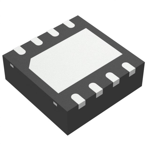
The IS31BL3212 is available in a Pb-free,
space-saving 2mm×2mm DFN-8 and SOT23-6
package.
Ultra low headroom voltage
Cost effective LED driver
Four channel constant current output ideal for
driving LEDs
Best noise and efficiency performance
Ultra low quiescent supply current: 1.0mA (Typ.)
Highly integrated design, minimal component
Low shutdown current: 1.0μA (Typ.)
APPLICATIONS
White LED display backlights
White LED keypad backlights
Cell Li-ion battery-operated equipment including
PDAs, hand-held PCs, cellular phone
TYPICAL APPLICATION CIRCUIT
Figure 1
Figure 2
Typical Application Circuit
Application Circuit for Less Than 4 LEDs
Note: If less than four LEDs connected, the left pin can be floating or connected to GND. Connecting to GND is recommended.
Integrated Silicon Solution, Inc. – www.issi.com
Rev. C, 06/24/2014
1
�IS31BL3212
PIN CONFIGURATION
Package
Pin Configuration (Top View)
DFN-8
EN/SET
1
6
D3
GND
2
5
D2
VCC
3
4
D1
SOT23-6
PIN DESCRIPTION
No.
Pin
Description
DFN-8
SOT23-6
1
-
D4
White LED channel.
2~4
6~4
D3~D1
White LED channel.
5
3
VCC
Power supply input.
6
2
GND
Ground.
7
1
EN/SET
8
-
NC
-
Thermal Pad
Serial digital input, control the output
current. Internal 500kΩ pull down resistor.
No connection.
Connect to GND.
Integrated Silicon Solution, Inc. – www.issi.com
Rev. C, 06/24/2014
2
�IS31BL3212
ORDERING INFORMATION
Industrial Range: -40°C to +85°C
Order Part No.
Package
IS31BL3212-DLS2-TR
DFN-8, Lead-free
IS31BL3212-STLS2-TR
SOT23-6, Lead-free
QTY/Reel
3000
Copyright © 2014 Integrated Silicon Solution, Inc. All rights reserved. ISSI reserves the right to make changes to this specification and its products at any
time without notice. ISSI assumes no liability arising out of the application or use of any information, products or services described herein. Customers are
advised to obtain the latest version of this device specification before relying on any published information and before placing orders for products.
Integrated Silicon Solution, Inc. does not recommend the use of any of its products in life support applications where the failure or malfunction of the
product can reasonably be expected to cause failure of the life support system or to significantly affect its safety or effectiveness. Products are not
authorized for use in such applications unless Integrated Silicon Solution, Inc. receives written assurance to its satisfaction, that:
a.) the risk of injury or damage has been minimized;
b.) the user assume all such risks; and
c.) potential liability of Integrated Silicon Solution, Inc is adequately protected under the circumstances
Integrated Silicon Solution, Inc. – www.issi.com
Rev. C, 06/24/2014
3
�IS31BL3212
ABSOLUTE MAXIMUM RATINGS
Supply voltage, VCC
EN/SET voltage to GND, VEN/SET
Maximum junction temperature, TJMAX
Storage temperature range, TSTG
Operating temperature range, TA
ESD (HBM)
ESD (CDM)
-0.3V ~ +6.0V
-0.3V ~ VCC+0.3V
150°C
-65°C ~ +150°C
−40°C ~ +85°C
3kV
1kV
Note:
Stresses beyond those listed under “Absolute Maximum Ratings” may cause permanent damage to the device. These are stress ratings only and
functional operation of the device at these or any other condition beyond those indicated in the operational sections of the specifications is not
implied. Exposure to absolute maximum rating conditions for extended periods may affect device reliability.
ELECTRICAL CHARACTERISTICS
TA = 25°C, unless otherwise noted. Typical values are TA = 25°C, VCC = 3.6V. (Note 1)
Symbol
Parameter
Condition
Min. Typ. Max. Unit
Input Power Supply
VCC
Operation range
2.7
5.5
V
IIN
Operating current
3.0 ≤ VCC ≤ 5.5, active no load,
current data = 1 (Note 2)
1.0
ISHDN
Shutdown current
VEN/SET = 0V
1.0
VHR
Minimum headroom voltage (DX)
IDX = 15mA, VCC = 3.3V
49
mV
VHR
Minimum headroom voltage (DX)
IDX= 20mA, VCC = 3.3V
60
mV
IDX
Output current regulation
Data = 1 (Note 2)
23
mA
VEN/SET(L)
Enable threshold low
VCC = 2.7V
VEN/SET(H)
Enable threshold high
VCC = 5.5V
tEN/SET LO
EN/SET low time
mA
2.6
μA
EN/SET
0.4
1.4
V
0.3
tEN/SET_HI_MIN Minimum EN/SET high time
(Note 3)
tEN/SET_HI_MAX Maximum EN/SET high time
(Note 3)
V
75
1.0
μs
μs
92
μs
tOFF
EN/SET off timeout
500
μs
tLAT
EN/SET latch timeout
500
μs
REN/SET DOWN EN/SET pull down resistor
(Note 3)
500
kΩ
Note 1: The IS31BL3212 is production tested at room temperature but guaranteed to meet performance specifications over other temperature
range by design, characterization, and correlation with statistical process controls.
Note 2: See PCC wire Serial Interface section in application information for more.
Note 3: Guaranteed by design.
Integrated Silicon Solution, Inc. – www.issi.com
Rev. C, 06/24/2014
4
�IS31BL3212
FUNCTIONAL BLOCK DIAGRAM
VCC
BG
EN/SET
IBias
Output
D1~D4
EN
Data
GND
Integrated Silicon Solution, Inc. – www.issi.com
Rev. C, 06/24/2014
5
�IS31BL3212
APPLICATION INFORMATION
OUTPUT CURRENT CAPABILITY
In order for the output currents to be regulated properly,
sufficient headroom voltage (VHR) is required. The
headroom voltage refers to the minimum amount of
voltage that must be present across the current source
in order to ensure the desired current is realizable. To
ensure the desired current is obtained, apply the
following equations to find the minimum input voltage
required:
VCC - VLEDX ≥ VHR
Notice that if less than four LEDs connected, the left
pin can be floating or connected to GND.
smooth transitions (e.g., to fade-out) or in abrupt steps,
giving the user complete programmability and
real-time control of LED brightness.
PCC WIRE SERIAL INTERFACE
The current level magnitude is controlled by Pulse
Count Control (PCC wire) serial interface. The
interface records rising edges of the EN/SET pin and
decodes them into 16 different states. The 16 current
level settings available are indicated in Table 1.
Table 1: Current Level Setting
Data
Output(mA/Ch)
Data
Output(mA/Ch)
1
23.0
9
5.8
The four constant current source outputs (D1 to D4)
can drive four individual LEDs with a maximum current
of 23mA each. The PCC wire serial interface enables
the IS31BL3212 and sets the current source
magnitudes.
2
19.6
10
4.8
3
16.1
11
4.1
4
13.8
12
3.5
5
11.8
13
2.8
CONSTANT CURRENT OUTPUT LEVEL SETTINGS
6
9.9
14
2.1
The constant current source levels for D1 to D4 are set
via the serial interface according to a logarithmic scale.
For the whole 16 codes, each code is approximately
1.5dB lower than the previous code. In this manner,
LED brightness appears linear with each increasing
code count. Because the outputs D1 to D4 are true
independent constant current sources, the voltage
observed on any single given output will be determined
by the actual forward voltage (VF) for the LED being
driven.
7
8.1
15
1.4
8
6.9
16
0.7
FUNCTIONAL DESCRIPTION
Since the output current sources of the IS31BL3212
are programmable, no PWM (pulse width modulation)
or additional control circuitry is needed to control LED
brightness. This feature greatly reduces the burden on
a microcontroller or system IC to manage LED or
display brightness, allowing the user to "set it and
forget it." With its high-speed serial interface (1MHz
data rate), the output current of the IS31BL3212 can
be changed successively to brighten or dim LEDs, in
Integrated Silicon Solution, Inc. – www.issi.com
Rev. C, 06/24/2014
The PCC wire serial interface has flexible timing.
After data is submitted, EN/SET is held high to latch
the data. Once EN/SET has been held in the logic high
state for time TLAT, the programmed current becomes
active and the internal data register is reset to zero.
For subsequent current level programming, the
number of rising edges corresponding to the desired
code must be entered on the EN/SET pin.
PCC WIRE SERIAL INTERFACE TIMING
When EN/SET is held low for an amount of time
greater than TOFF, the IS31BL3212 enters into
shutdown mode and draws 1.0µA typically from VCC.
The internal data register is reset to zero during
shutdown.
6
�IS31BL3212
LED SELECTION
THERMAL PROTECTION
The IS31BL3212 has low headroom voltage and it is
designed to drive white-LEDs.
The IS31BL3212 has a thermal protection circuit that
will shut down the chip if the die temperature rises
above the thermal limit.
The drive current will automatically scale down to
reduce the LED current consumption.
INPUT CAPACITOR SELECTION
The IS31BL3212 is designed to run off of a fixed input
voltage. Depending on the stability and condition of
this voltage rail, it may be necessary to add a small
input capacitor to help filter out any noise that may be
present on the line. In the event that filtering is needed,
ceramic composition capacitors are highly recommended over all other types of capacitors for use with
the IS31BL3212. Ceramic capacitors offer many
advantages over their tantalum and aluminum
electrolytic counterparts. A ceramic capacitor typically
has very low ESR, is lowest cost, has a smaller PCB
footprint, and is non-polarized. Low ESR ceramic
capacitors help to maximize charge pump transient
response. Since ceramic capacitors are non-polarized,
they are not prone to incorrect connection damage.
Integrated Silicon Solution, Inc. – www.issi.com
Rev. C, 06/24/2014
Although the IS31BL3212 is designed for driving white
LEDs, the device also can be used to drive most types
of LEDs with forward voltage specifications ranging
from 2.0V to 4.7V. LED applications may include main
and sub-LCD display backlighting, camera photo-flash
applications, color (RGB) LEDs, infrared (IR) diodes
for remotes, and other loads benefiting from a
controlled output current generated from a varying
input voltage. Since the D1 to D4 output current
sources are matched with negligible voltage
dependence, the LED brightness will be matched
regardless of the specific LED forward voltage (VF)
levels. In some instances (e.g., in high luminous output
applications such as photo flash), it may be necessary
to drive high-VF type LEDs. The low dropout current
sources in the IS31BL3212 make it capable of driving
LEDs with forward voltages as high as 4.7V at full
current from an input supply of 2.7V to 5.0V. Outputs
can be paralleled to drive high-current LEDs without
complication
7
�IS31BL3212
CLASSIFICATION REFLOW PROFILES
Profile Feature
Pb-Free Assembly
Preheat & Soak
Temperature min (Tsmin)
Temperature max (Tsmax)
Time (Tsmin to Tsmax) (ts)
150°C
200°C
60-120 seconds
Average ramp-up rate (Tsmax to Tp)
3°C/second max.
Liquidous temperature (TL)
Time at liquidous (tL)
217°C
60-150 seconds
Peak package body temperature (Tp)*
Max 260°C
Time (tp)** within 5°C of the specified
classification temperature (Tc)
Max 30 seconds
Average ramp-down rate (Tp to Tsmax)
6°C/second max.
Time 25°C to peak temperature
8 minutes max.
Figure 3
Classification Profile
Integrated Silicon Solution, Inc. – www.issi.com
Rev. C, 06/24/2014
8
�IS31BL3212
PACKAGE INFORMATION
DFN-8
Integrated Silicon Solution, Inc. – www.issi.com
Rev. C, 06/24/2014
9
�IS31BL3212
SOT23-6
Note: All dimensions in millimeters unless otherwise stated.
Integrated Silicon Solution, Inc. – www.issi.com
Rev. C, 06/24/2014
10
�


 工商网监
湘ICP备2023018690号
工商网监
湘ICP备2023018690号
