Advanced Science And Novel Technology Company, Inc.
2790 Skypark Drive Suite 112, Torrance, CA 90505
Offices: 310-530-9400 / Fax: 310-530-9402
www.adsantec.com
ASNT5117-KMC
DC-40 Gbps D-Type Flip-Flop with Amplitude Adjust
High speed broadband D-Type Flip-Flop for data retiming with full rate clock
Input data common mode control
Exhibits low jitter and limited temperature variation over industrial temperature range
4ps set-up/hold time capability
88% clock phase margin for retiming of data input eye
Fully differential CML input interfaces
Fully differential CML output interface with adjustable 0 to 900mV single-ended swing
Single +3.3V or -3.3V power supply
Power consumption: 726mW
Fabricated in SiGe for high performance, yield, and reliability
Custom CQFP 24-pin package
Rev. 1.3.2
1
February 2020
�Advanced Science And Novel Technology Company, Inc.
2790 Skypark Drive Suite 112, Torrance, CA 90505
Offices: 310-530-9400 / Fax: 310-530-9402
www.adsantec.com
DESCRIPTION
ampadj vcc
vcc dccd
50
50
dp
DFF
core
dn
outp
outn
50
50
vcc
50
50
vcc
vcc
vcc
cp cn
Fig. 1. Functional Block Diagram
The temperature stable ASNT5117-KMC SiGe IC provides broadband data retiming functionality and is
intended for use in high-speed measurement / test equipment. The IC shown in Fig. 1 can sample a highspeed data signal dp/dn with a full-rate external clock cp/cn to create a full-rate retimed NRZ data output
qp/qn. The internal DC common mode voltage levels on data inputs dp/dn can be adjusted by applying
analog voltage to the control input dccd. The output amplitude of the DFF is adjustable by using the
control voltage ampadj.
The part’s I/O’s support the CML logic interface with on chip equivalent 50Ohm termination and may be
used differentially, AC/DC coupled, single-ended, or in any combination (see also POWER SUPPLY
CONFIGURATION).
HS Clock Input Buffer
The buffer can accept high-speed signals at its differential CML input port cp/cn. It can also accept a
single-ended signal with a threshold voltage applied to the unused pin. It can handle a wide range of input
signal amplitudes. The buffer utilizes on-chip single-ended 50Ohm termination to vcc for each input line.
HS Data Input Buffer
The buffer can accept high-speed signals at its differential CML input port dp/dn. It can also accept a
single-ended signal with a threshold voltage applied to the unused pin. It can handle a wide range of input
signal amplitudes. The buffer utilizes on-chip single-ended 50Ohm termination to vcc for each input line.
The buffer allows for adjustment of its input DC common-mode voltage by changing the control voltage
dccd following the diagram shown in Fig. 2. Here the x-axis presents the dccd values, the y-axis presents
the common-mode voltage values, the red lines correspond to the dp input, the blue lines correspond to
Rev. 1.3.2
2
February 2020
�Advanced Science And Novel Technology Company, Inc.
2790 Skypark Drive Suite 112, Torrance, CA 90505
Offices: 310-530-9400 / Fax: 310-530-9402
www.adsantec.com
the dn input, and the solid lines represent typical conditions while dotted and dashed lines represent slow
and fast conditions respectively.
Fig. 2. Duty Cycle Control Diagram
HS Data Output Buffer
The buffer receives high-speed serial data from the DFF core and converts it into a differential CML
output signal qp/qn. Each buffer utilizes internal single-ended 50Ohm loads to vcc and requires singleended 50Ohm external termination. The termination resistors can be connected from each output directly
to vcc, or through DC blocks to vee. The amplitude of the output signals can be adjusted from 0V to its
maximum value using the external control voltage ampadj.
POWER SUPPLY CONFIGURATION
The part can operate with either a negative supply (vcc = 0.0V = ground and vee = −3.3V), or a positive
supply (vcc = +3.3V and vee = 0.0V = ground). In case of a positive supply, all I/Os need AC termination
when connected to any devices with 50Ohm termination to ground. Different PCB layouts will be needed
for each different power supply combination.
All the characteristics detailed below assume vcc = 0.0V and vee = -3.3V.
ABSOLUTE MAXIMUM RATINGS
Caution: Exceeding the absolute maximum ratings shown in Table 1 may cause damage to this product
and/or lead to reduced reliability. Functional performance is specified over the recommended operating
conditions for power supply and temperature only. AC and DC device characteristics at or beyond the
absolute maximum ratings are not assumed or implied. All min and max voltage limits are referenced to
ground (assumed vcc).
Rev. 1.3.2
3
February 2020
�Advanced Science And Novel Technology Company, Inc.
2790 Skypark Drive Suite 112, Torrance, CA 90505
Offices: 310-530-9400 / Fax: 310-530-9402
www.adsantec.com
Parameter
Min
Max
Supply Voltage (vee)
-3.6
Power Consumption
0.80
Input Data Voltage Swing (SE)
1.0
Input Clk Voltage Swing (SE)
1.0
Case Temperature
+90
Storage Temperature
-40
+100
Operational Humidity
10
98
Storage Humidity
10
98
Table 1. Absolute Maximum Ratings
Units
V
W
V
V
ºC
ºC
%
%
TERMINAL FUNCTIONS
TERMINAL
Name No. Type
dp
dn
cp
cn
qp
qn
21
23
3
5
11
9
ampadj
dccd
Name
vcc
vee
Rev. 1.3.2
Pin
Default
function
state
High-Speed I/Os
Input data
CML
Input
CML Input clock
Input
CML Output data.
Output
Termination
SE 50Ohm to vcc
SE 50Ohm to vcc
SE 50Ohm to vcc. Require
external SE 50Ohm to vcc
DC Controls
15 Analog Output data amplitude
2.3KOhm to vcc, 9.3KOhm
voltage control
to vee
17
Input data common
5.6KOhm to vcc, 22.2KOhm
mode voltage control
to vee
Supply and Termination Voltages
Description
Pin Number
Positive power supply
2, 4, 6, 8, 10, 12, 14, 16, 18, 20, 22, 24
(+3.3V or 0V)
Negative power supply
1, 7, 13, 19
(0V or -3.3V)
4
February 2020
�Advanced Science And Novel Technology Company, Inc.
2790 Skypark Drive Suite 112, Torrance, CA 90505
Offices: 310-530-9400 / Fax: 310-530-9402
www.adsantec.com
ELECTRICAL CHARACTERISTICS
PARAMETER
vcc
vee
Ivcc
Power consumption
Junction temperature
Data rate
Swing
CM Voltage Level
Frequency
Swing
CM Voltage Level
Duty Cycle
Clock phase margin
Data rate
Logic “1” level
Logic “0” level
Jitter
Max level
Min level
MIN
TYP
MAX
UNIT
COMMENTS
General Parameters
0.0
V
External ground
-3.1
-3.3
-3.5
V
±6%
220
233
mA
726
770
mW
-25
50
125
°C
HS Input Data (dp/dn)
DC
32
40
Gbps
0.05
0.8
V
Differential or SE, p-p
vcc-0.7+sw/2 vcc+0.6-sw/2
V
Must match for both inputs
HS Input Clock (cp/cn)
DC
32
40
GHz
0.05
0.8
V
Differential or SE, p-p
vcc-0.7
vcc+0.6-sw/2
V
Must match for both inputs
40
50
60
%
86
88
90
%
For reliable data latching
HS Output Data (qp/qn)
DC
32
40
Gbps
vcc-0.05 vcc-0.03 vcc-0.01
V
Equal to logic “1”
V
With ampadj set at minimum
vcc-0.42 vcc-0.40 vcc-0.38
V
With ampadj set at default
vcc-0.90 vcc-0.80 vcc-0.78
V
With ampadj set at maximum
1.5
ps
Peak-to-peak at 32Gbps
DC Input Controls (dccd, ampadj)
V
vcc
vcc - 1.3
V
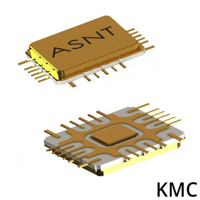
PACKAGE INFORMATION
The chip die is housed in a custom 24-pin CQFP package shown in Fig. 3. The package provides a center
heat slug located on its back side to be used for heat dissipation. ADSANTEC recommends for this
section to be soldered to the vcc plain, which is ground for a negative supply, or power for a positive
supply.
The part’s identification label is ASNT5117-KMC. The first 8 characters of the name before the dash
identify the bare die including general circuit family, fabrication technology, specific circuit type, and part
version while the 3 characters after the dash represent the package’s manufacturer, type, and pin out
count.
This device complies with the Restriction of Hazardous Substances (RoHS) per 2011/65/EU for all ten
substances.
Rev. 1.3.2
5
February 2020
�Advanced Science And Novel Technology Company, Inc.
2790 Skypark Drive Suite 112, Torrance, CA 90505
Offices: 310-530-9400 / Fax: 310-530-9402
www.adsantec.com
Fig. 3. CQFP 24-Pin Package Drawing (All Dimensions in mm)
Rev. 1.3.2
6
February 2020
�Advanced Science And Novel Technology Company, Inc.
2790 Skypark Drive Suite 112, Torrance, CA 90505
Offices: 310-530-9400 / Fax: 310-530-9402
www.adsantec.com
REVISION HISTORY
Revision
1.3.2
1.2.2
1.2.1
Date
02-2020
07-2019
10-2015
1.1.1
04-2015
1.0.1
04-2015
Rev. 1.3.2
Changes
Updated Package Information
Updated Letterhead
Corrected electrical characteristics section
Updated package information section
Updated maximum frequency of operation
Updated maximum output amplitude
First release
7
February 2020
�


 工商网监
湘ICP备2023018690号
工商网监
湘ICP备2023018690号
