Important notice
Dear Customer,
On 7 February 2017 the former NXP Standard Product business became a new company with the
tradename Nexperia. Nexperia is an industry leading supplier of Discrete, Logic and PowerMOS
semiconductors with its focus on the automotive, industrial, computing, consumer and wearable
application markets
In data sheets and application notes which still contain NXP or Philips Semiconductors references, use
the references to Nexperia, as shown below.
Instead of http://www.nxp.com, http://www.philips.com/ or http://www.semiconductors.philips.com/,
use http://www.nexperia.com
Instead of sales.addresses@www.nxp.com or sales.addresses@www.semiconductors.philips.com, use
salesaddresses@nexperia.com (email)
Replace the copyright notice at the bottom of each page or elsewhere in the document, depending on
the version, as shown below:
- © NXP N.V. (year). All rights reserved or © Koninklijke Philips Electronics N.V. (year). All rights
reserved
Should be replaced with:
- © Nexperia B.V. (year). All rights reserved.
If you have any questions related to the data sheet, please contact our nearest sales office via e-mail
or telephone (details via salesaddresses@nexperia.com). Thank you for your cooperation and
understanding,
Kind regards,
Team Nexperia
�DISCRETE SEMICONDUCTORS
DATA SHEET
dbook, halfpage
MBD127
BZA800A-series
Quadruple ESD transient voltage
suppressor
Product data sheet
Supersedes data of 2000 May 01
2000 Sep 25
�NXP Semiconductors
Product data sheet
Quadruple ESD transient voltage
suppressor
BZA800A-series
FEATURES
PINNING
• ESD rating >8 kV, according to IEC1000-4-2
PIN
DESCRIPTION
• SOT353 (SC-88A) surface mount package
1
cathode 1
• Common anode configuration.
2
common anode
3
cathode 2
APPLICATIONS
4
cathode 3
• Computers and peripherals
5
cathode 4
• Audio and video equipment
• Communication systems.
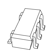
DESCRIPTION
handbook, halfpage5
Monolithic transient voltage suppressor diode in a five lead
SOT353 (SC-88A) package for 4-bit wide ESD transient
suppression.
4
1
3
2
4
MARKING
5
1
TYPE NUMBER
MARKING CODE
BZA856A
Z1
BZA862A
Z2
BZA868A
Z3
BZA820A
Z4
2000 Sep 25
2
3
MGT580
Fig.1 Simplified outline SOT353 (SC-88A).
2
�NXP Semiconductors
Product data sheet
Quadruple ESD transient voltage
suppressor
BZA800A-series
LIMITING VALUES
In accordance with the Absolute Maximum Rating System (IEC 60134).
SYMBOL
PARAMETER
CONDITIONS
MIN.
MAX.
UNIT
Per diode
IZ
working current
Tamb = 25 °C
−
note 1
mA
IF
continuous forward current
Tamb = 25 °C
−
200
mA
IFSM
non-repetitive peak forward current tp = 1 ms; square pulse
−
3.75
A
Ptot
total power dissipation
Tamb = 25 °C
−
335
mW
PZSM
non repetitive peak reverse power
dissipation:
square pulse; tp = 1 ms; see Fig.3
BZA856A, BZA862A, BZA868A,
−
24
W
BZA820A
−
17
W
Tstg
storage temperature
−65
+150
°C
Tj
junction temperature
−
150
°C
Note
1. DC working current limited by Ptot(max).
THERMAL CHARACTERISTICS
SYMBOL
Rth j-a
2000 Sep 25
PARAMETER
CONDITIONS
thermal resistance from junction to ambient
all diodes loaded
3
VALUE
UNIT
370
K/W
�NXP Semiconductors
Product data sheet
Quadruple ESD transient voltage
suppressor
BZA800A-series
ELECTRICAL CHARACTERISTICS
Tj = 25 °C unless otherwise specified.
SYMBOL
PARAMETER
Cd
V
BZA856A
VR = 3 V
−
−
2 000
nA
BZA862A
VR = 4 V
−
−
700
nA
BZA868A
VR = 4.3 V
−
−
200
nA
BZA820A
VR = 15 V
−
−
100
nA
BZA856A
5.32
5.6
5.88
V
BZA862A
5.89
6.2
6.51
V
BZA868A
6.46
6.8
7.14
V
BZA820A
19
20
21
V
BZA856A
−
−
400
Ω
BZA862A
−
−
300
Ω
BZA868A
−
−
200
Ω
BZA820A
−
−
125
Ω
BZA856A
−
−0.2
−
mV/K
BZA862A
−
1.8
−
mV/K
BZA868A
−
3
−
mV/K
BZA820A
−
16
−
mV/K
BZA856A
−
−
240
pF
BZA862A
−
−
200
pF
BZA868A
−
−
180
pF
−
−
50
pF
BZA856A
−
−
3.2
A
BZA862A
−
−
2.9
A
BZA868A
−
−
2.6
A
BZA820A
−
−
0.6
A
working voltage
differential resistance
temperature coefficient
diode capacitance
non-repetitive peak reverse current
2000 Sep 25
UNIT
1.3
IZ = 1 mA
IZ = 1 mA
IZ = 1 mA
f = 1 MHz; VR = 0
BZA820A
IZSM
MAX.
−
reverse current
SZ
TYP.
−
forward voltage
IR
rdiff
MIN.
IF = 200 mA
VF
VZ
CONDITIONS
tp = 1 ms; Tamb = 25 °C
4
�NXP Semiconductors
Product data sheet
Quadruple ESD transient voltage
suppressor
BZA800A-series
MGT583
10
MGT584
102
handbook, halfpage
handbook, halfpage
BZA856A
BZA856A, BZA862A, BZA868A
I ZSM
(A)
PZSM
(W)
BZA862A
BZA820A
BZA868A
1
10
BZA820A
10−1
10−2
10−1
1
t p (ms)
1
10−2
10
10−1
1
t p (ms)
10
PZSM = VZSM × IZSM.
VZSM is the non-repetitive peak reverse voltage at IZSM.
Fig.3
Fig.2
Maximum non-repetitive peak reverse
power dissipation as a function of pulse
duration (square pulse).
Maximum non-repetitive peak reverse
current as a function of pulse time.
MGT586
MGT585
400
200
Cd
handbook, halfpage
handbook, halfpage
Ptot
(mW)
(pF)
160
300
120
200
BZA856A
80
BZA862A
BZA868A
100
40
BZA820A
0
0
5
10
VR (V)
0
15
0
50
100
Tamb (°C)
Tj = 25 °C; f = 1 MHz.
Fig.4
Diode capacitance as a function of reverse
voltage; typical values.
2000 Sep 25
Fig.5 Power derating curve.
5
150
�NXP Semiconductors
Product data sheet
Quadruple ESD transient voltage
suppressor
handbook, full pagewidth
ESD TESTER
RZ
450 Ω
BZA800A-series
RG 223/U
50 Ω coax
CZ
10×
ATTENUATOR
DIGITIZING
OSCILLOSCOPE
50 Ω
note 1
1/4 BZA800A
IEC 1000-4-2 network
CZ = 150 pF; RZ = 330 Ω
Note 1: attenuator is only used for open
socket high voltage measurements
vertical scale = 100 V/div
horizontal scale = 50 ns/div
BZA820A
GND-4
BZA868A
GND-3
BZA862A
GND-2
BZA856A
GND-1
GND
unclamped +1 kV ESD voltage waveform
(IEC 1000-4-2 network)
vertical scale = 10 V/div
horizontal scale = 50 ns/div
clamped +1 kV ESD voltage waveform
(IEC 1000-4-2 network)
GND
GND
vertical scale = 100 V/div
horizontal scale = 50 ns/div
vertical scale = 10 V/div
horizontal scale = 50 ns/div
unclamped −1 kV ESD voltage waveform
(IEC 1000-4-2 network)
clamped −1 kV ESD voltage waveform
(IEC 1000-4-2 network)
Fig.6 ESD clamping test set-up and waveforms.
2000 Sep 25
6
MGT587
�NXP Semiconductors
Product data sheet
Quadruple ESD transient voltage
suppressor
BZA800A-series
APPLICATION INFORMATION
Typical common anode application
A quadruple transient suppressor in a SOT353 package makes it possible to protect four separate lines using only one
package. Two simplified examples are shown in Figs 7 and 8.
handbook, full pagewidth
keyboard,
terminal,
printer,
etc.
A
B
C
D
I/O
FUNCTIONAL
DECODER
BZA800A
GND
MGT581
Fig.7 Computer interface protection.
VDD
handbook, full pagewidth
VGG
address bus
RAM
I/O
ROM
data bus
CPU
CLOCK
control bus
BZA800A
GND
MGT582
Fig.8 Microprocessor protection.
2000 Sep 25
7
�NXP Semiconductors
Product data sheet
Quadruple ESD transient voltage
suppressor
BZA800A-series
Device placement and printed-circuit board layout
Circuit board layout is of extreme importance in the
suppression of transients. The clamping voltage of the
BZA800A is determined by the peak transient current and
the rate of rise of that current (di/dt). Since parasitic
inductances can further add to the clamping voltage
(V = L di/dt) the series conductor lengths on the
printed-circuit board should be kept to a minimum. This
includes the lead length of the suppression element.
In addition to minimizing conductor length the following
printed-circuit board layout guidelines are recommended:
1. Place the suppression element close to the input
terminals or connectors
2. Keep parallel signal paths to a minimum
3. Avoid running protection conductors in parallel with
unprotected conductors
4. Minimize all printed-circuit board loop areas including
power and ground loops
5. Minimize the length of the transient return path to
ground
6. Avoid using shared transient return paths to a common
ground point.
2000 Sep 25
8
�NXP Semiconductors
Product data sheet
Quadruple ESD transient voltage
suppressor
BZA800A-series
PACKAGE OUTLINE
Plastic surface mounted package; 5 leads
SOT353
D
E
B
y
X
A
HE
5
v M A
4
Q
A
A1
1
2
e1
3
bp
c
Lp
w M B
e
detail X
0
1
2 mm
scale
DIMENSIONS (mm are the original dimensions)
UNIT
A
A1
max
bp
c
D
E (2)
e
e1
HE
Lp
Q
v
w
y
mm
1.1
0.8
0.1
0.30
0.20
0.25
0.10
2.2
1.8
1.35
1.15
1.3
0.65
2.2
2.0
0.45
0.15
0.25
0.15
0.2
0.2
0.1
OUTLINE
VERSION
SOT353
2000 Sep 25
REFERENCES
IEC
JEDEC
EIAJ
SC-88A
9
EUROPEAN
PROJECTION
ISSUE DATE
97-02-28
�NXP Semiconductors
Product data sheet
Quadruple ESD transient voltage
suppressor
BZA800A-series
DATA SHEET STATUS
DOCUMENT
STATUS(1)
PRODUCT
STATUS(2)
DEFINITION
Objective data sheet
Development
This document contains data from the objective specification for product
development.
Preliminary data sheet
Qualification
This document contains data from the preliminary specification.
Product data sheet
Production
This document contains the product specification.
Notes
1. Please consult the most recently issued document before initiating or completing a design.
2. The product status of device(s) described in this document may have changed since this document was published
and may differ in case of multiple devices. The latest product status information is available on the Internet at
URL http://www.nxp.com.
above those given in the Characteristics sections of this
document is not implied. Exposure to limiting values for
extended periods may affect device reliability.
DISCLAIMERS
General ⎯ Information in this document is believed to be
accurate and reliable. However, NXP Semiconductors
does not give any representations or warranties,
expressed or implied, as to the accuracy or completeness
of such information and shall have no liability for the
consequences of use of such information.
Terms and conditions of sale ⎯ NXP Semiconductors
products are sold subject to the general terms and
conditions of commercial sale, as published at
http://www.nxp.com/profile/terms, including those
pertaining to warranty, intellectual property rights
infringement and limitation of liability, unless explicitly
otherwise agreed to in writing by NXP Semiconductors. In
case of any inconsistency or conflict between information
in this document and such terms and conditions, the latter
will prevail.
Right to make changes ⎯ NXP Semiconductors
reserves the right to make changes to information
published in this document, including without limitation
specifications and product descriptions, at any time and
without notice. This document supersedes and replaces all
information supplied prior to the publication hereof.
No offer to sell or license ⎯ Nothing in this document
may be interpreted or construed as an offer to sell products
that is open for acceptance or the grant, conveyance or
implication of any license under any copyrights, patents or
other industrial or intellectual property rights.
Suitability for use ⎯ NXP Semiconductors products are
not designed, authorized or warranted to be suitable for
use in medical, military, aircraft, space or life support
equipment, nor in applications where failure or malfunction
of an NXP Semiconductors product can reasonably be
expected to result in personal injury, death or severe
property or environmental damage. NXP Semiconductors
accepts no liability for inclusion and/or use of NXP
Semiconductors products in such equipment or
applications and therefore such inclusion and/or use is at
the customer’s own risk.
Export control ⎯ This document as well as the item(s)
described herein may be subject to export control
regulations. Export might require a prior authorization from
national authorities.
Quick reference data ⎯ The Quick reference data is an
extract of the product data given in the Limiting values and
Characteristics sections of this document, and as such is
not complete, exhaustive or legally binding.
Applications ⎯ Applications that are described herein for
any of these products are for illustrative purposes only.
NXP Semiconductors makes no representation or
warranty that such applications will be suitable for the
specified use without further testing or modification.
Limiting values ⎯ Stress above one or more limiting
values (as defined in the Absolute Maximum Ratings
System of IEC 60134) may cause permanent damage to
the device. Limiting values are stress ratings only and
operation of the device at these or any other conditions
2000 Sep 25
10
�NXP Semiconductors
Customer notification
This data sheet was changed to reflect the new company name NXP Semiconductors. No changes were
made to the content, except for the legal definitions and disclaimers.
Contact information
For additional information please visit: http://www.nxp.com
For sales offices addresses send e-mail to: salesaddresses@nxp.com
© NXP B.V. 2009
All rights are reserved. Reproduction in whole or in part is prohibited without the prior written consent of the copyright owner.
The information presented in this document does not form part of any quotation or contract, is believed to be accurate and reliable and may be changed
without notice. No liability will be accepted by the publisher for any consequence of its use. Publication thereof does not convey nor imply any license
under patent- or other industrial or intellectual property rights.
Printed in The Netherlands
613514/03/pp11
Date of release: 2000 Sep 25
Document order number: 9397 750 07142
�


 工商网监
湘ICP备2023018690号
工商网监
湘ICP备2023018690号