IRFR5305
P-Channel 60 V (D-S) MOSFET
FEATURES
PRODUCT SUMMARY
VDS (V)
- 60
RDS(on) ()
ID (A)
0.020 at VGS = - 10 V
- 50
0.025 at VGS = - 4.5 V
- 45
• TrenchFET® Power MOSFET
• Material categorization:
APPLICATIONS
• Load Switch
JS
TO-252
S
MI
G
CR
S
O
D
G
D
Top View
P-Channel MOSFET
mi
Se
ABSOLUTE MAXIMUM RATINGS (TA = 25 °C, unless otherwise noted)
Parameter
Gate-Source Voltage
Limit
VDS
- 60
VGS
± 20
ID
- 50
- 40
IDM
- 160
IAS
- 50
TC = 25 °C
TC = 125 °C
Pulsed Drain Current
Avalanche Current
uc
Energya
nd
Continuous Drain Current (TJ = 175 °C)
Single Pulse Avalanche
Symbol
co
Drain-Source Voltage
EAS
L = 0.1 mH
TC = 25 °C
Power Dissipation
A
125
mJ
W
2.5b, c
TJ, Tstg
to
Operating Junction and Storage Temperature Range
V
113c
PD
TA = 25 °C
Unit
Symbol
Typical
Maximum
15
18
- 55 to 150
°C
r
THERMAL RESISTANCE RATINGS
Parameter
t 10 s
Junction-to-Ambientb
Steady State
RthJA
RthJC
Junction-to-Case
40
50
0.82
1.1
Unit
°C/W
Notes:
a. Duty cycle 1 %.
b. When mounted on 1" square PCB (FR-4 material).
c. See SOA curve for voltage derating.
d. Package limited.
www.jsmsemi.com
第1/6页
�IRFR5305
P-Channel 60 V (D-S) MOSFET
SPECIFICATIONS (TJ = 25 °C, unless otherwise noted)
Parameter
Symbol
Test Conditions
Min.
VDS
VGS = 0 V, ID = - 250 µA
- 60
VGS(th)
VDS = VGS, ID = - 250 µA
- 1.5
IGSS
VDS = 0 V, VGS = ± 20 V
Typ.
Max.
Unit
Static
Drain-Source Breakdown Voltage
Gate Threshold Voltage
Gate-Body Leakage
IDSS
Zero Gate Voltage Drain Current
On-State Drain Currenta
JS
Forward Transconductance
-1
VDS = - 60 V, VGS = 0 V, TJ = 125 °C
- 50
VDS = - 60 V, VGS = 0 V, TJ = 150 °C
- 100
VDS = -5 V, VGS = - 10 V
RDS(on)
Dynamic
VGS = - 10 V, ID = - 40 A, TJ = 150 °C
0.035
VGS = - 4.5 V, ID = - 14 A
0.025
VDS = - 15 V, ID = - 17 A
61
Ciss
Input Capacitance
Total Gate Chargec
Crss
305
Qg
110
Gate-Drain Chargec
Qgd
Turn-On Delay Timec
td(on)
c
tr
Turn-Off Delay Timec
td(off)
Rise Time
165
nC
19
15
23
70
105
175
260
Ω
175
260
tf
IS
pF
VDD = - 30 V, RL = 0.6 Ω
ID ≅ - 40 A, VGEN = - 10 V, RG = 6
Source-Drain Diode Ratings and Characteristics TC = 25
Continuous Current
S
28
°Cb
co
Fall Timec
VDS = - 30 V, VGS = - 10 V, ID = - 40 A
mi
Gate-Source Charge
Qgs
0.040
380
Se
c
VGS = 0 V, VDS = - 25 V, f = 1 MHz
O
Reverse Transfer Capacitance
µA
2950
Coss
Output Capacitance
nA
0.025
0.030
gfs
V
A
0.020
VGS = - 10 V, ID = - 40 A, TJ = 125 °C
CR
b
- 50
VGS = - 10 V, ID = - 17 A
MI
a
± 100
VDS = - 60 V, VGS = 0 V
ID(on)
Drain-Source On-State Resistancea
-3
- 40
ns
nd
A
Pulsed Current
ISM
Forward Voltagea
VSD
IF = - 40 A, VGS = 0 V
-1
- 1.6
V
trr
IF = - 40 A, dI/dt = 100 A/µs
45
70
ns
r
to
Notes:
a. Pulse test; pulse width 300 µs, duty cycle 2 %.
b. Guaranteed by design, not subject to production testing.
c. Independent of operating temperature.
uc
Reverse Recovery Time
- 80
Stresses beyond those listed under “Absolute Maximum Ratings” may cause permanent damage to the device. These are stress ratings only, and functional operation
of the device at these or any other conditions beyond those indicated in the operational sections of the specifications is not implied. Exposure to absolute maximum
rating conditions for extended periods may affect device reliability.
www.jsmsemi.com
第2/6页
�IRFR5305
P-Channel 60 V (D-S) MOSFET
TYPICAL CHARACTERISTICS (25 °C, unless otherwise noted)
80
80
VGS = 10 thru 4 V
70
70
60
I D - Drain Current (A)
I D - Drain Current (A)
60
50
40
30
3V
20
50
40
30
TC = 125 ° C
20
JS
10
0
1
- 55 °C
MI
0
25 ° C
10
2
3
4
0
0.0
5
0.5
VDS - Drain-to-Source Voltage (V)
60
3.0
3.5
4.0
70
80
0.050
0.040
VGS = 4.5 V
mi
R DS(on) - On-Resistance (Ω)
125 °C
Se
40
20
0.030
VGS = 10 V
0.020
co
g fs - Transconductance (S)
2.5
25 °C
80
0.000
0
10
20
30
40
50
nd
0
0
60
VGS - Gate-to-Source Voltage (V)
10
Ciss
2000
1500
1000
Coss
Crss
0
40
50
60
ID - Drain Current (A)
VDS = 30 V
ID = 40 A
8
r
VGS - Gate-to-Source Voltage (V)
3000
0
30
to
3500
500
20
uc
4000
2500
10
On-Resistance vs. Drain Current
Transconductance
C - Capacitance (pF)
2.0
0.060
O
TC = - 55 °C
1.5
Transfer Characteristics
CR
Output Characteristics
100
1.0
VGS - Gate-to-Source Voltage (V)
6
4
2
0
10
20
30
40
50
60
0
VDS - Drain-to-Source Voltage (V)
20
40
60
80
100
120
Qg - Total Gate Charge (nC)
Capacitance
Gate Charge
www.jsmsemi.com
第3/6页
�IRFR5305
P-Channel 60 V (D-S) MOSFET
TYPICAL CHARACTERISTICS
100
1.8
I S - Source Current (A)
VGS = 10 V
ID = 17 A
1.6
1.4
1.2
1.0
0.8
0.6
- 50
- 25
0
MI
JS
R DS(on) - On-Resistance (Normalized)
2.0
25
50
75
TJ = 150 °C
TJ = 25 °C
10
1
100
125
0.0
150
0.6
1.2
0.3
0.9
VSD - Source-to-Drain Voltage (V)
TJ - Junction Temperature (°C)
1.5
CR
Source-Drain Diode Forward Voltage
On-Resistance vs. Junction Temperature
THERMAL RATINGS (25 °C, unless otherwise noted)
100
O
50
Limited by R DS(on)*
30
P(t) = 0.0001
10
BVDSS
Limited
mi
I D - Drain Current (A)
Se
20
10
P(t) = 0.001
co
I D - Drain Current (A)
40
5
0
25
50
75
100
125
1
0.1
1
10
100
VDS - Drain-to-Source Voltage (V)
* VGS > minimum VGS at which RDS(on) is specified
uc
TC - Case Temperature (°C)
150
P(t) = 0.1
P(t) = 1
nd
0
Drain Current vs. Case Temperature
Safe Operating Area
to
2
1
Duty Cycle = 0.5
r
Normalized Effective Transient
Thermal Impedance
P(t) = 0.01
TC = 25 °C
Single Pulse
0.2
0.1
0.1
0.05
0.02
Single Pulse
0.01
10 -4
10 -3
10 -2
Square Wave Pulse Duration (s)
10 -1
1
Normalized Thermal Transient Impedance, Junction-to-Case
www.jsmsemi.com
第4/6页
�IRFR5305
P-Channel 60 V (D-S) MOSFET
TO-252AA CASE OUTLINE
E
MILLIMETERS
A
C2
H
D
L3
b3
b2
CR
e1
L
gage plane height (0.5 mm)
L4
MI
e
L5
JS
b
C
A1
D1
O
MIN.
MAX.
MIN.
MAX.
A
2.18
2.38
0.086
0.094
A1
-
0.127
-
0.005
b
0.64
0.88
0.025
0.035
b2
0.76
1.14
0.030
0.045
b3
4.95
5.46
0.195
0.215
C
0.46
0.61
0.018
0.024
C2
0.46
0.89
0.018
0.035
D
5.97
6.22
0.235
0.245
D1
5.21
-
0.205
0.265
E
6.35
6.73
0.250
E1
4.32
-
0.170
-
H
9.40
10.41
0.370
0.410
e
2.28 BSC
0.090 BSC
e1
4.56 BSC
0.180 BSC
L
1.40
1.78
0.055
0.070
L3
0.89
1.27
0.035
0.050
L4
-
1.02
-
0.040
L5
1.14
1.52
0.045
0.060
ECN: X12-0247-Rev. M, 24-Dec-12
DWG: 5347
mi
Se
E1
INCHES
DIM.
Note
• Dimension L3 is for reference only.
co
r
to
uc
nd
www.jsmsemi.com
第5/6页
�IRFR5305
P-Channel 60 V (D-S) MOSFET
RECOMMENDED MINIMUM PADS FOR DPAK (TO-252)
0.224
0.243
(10.668)
0.420
mi
0.087
(2.202)
Se
0.090
O
0.180
0.055
co
(4.572)
(2.286)
CR
MI
JS
(6.180)
(5.690)
(1.397)
r
to
uc
nd
Recommended Minimum Pads
Dimensions in Inches/(mm)
www.jsmsemi.com
第6/6页
�
很抱歉,暂时无法提供与“IRFR5305”相匹配的价格&库存,您可以联系我们找货
免费人工找货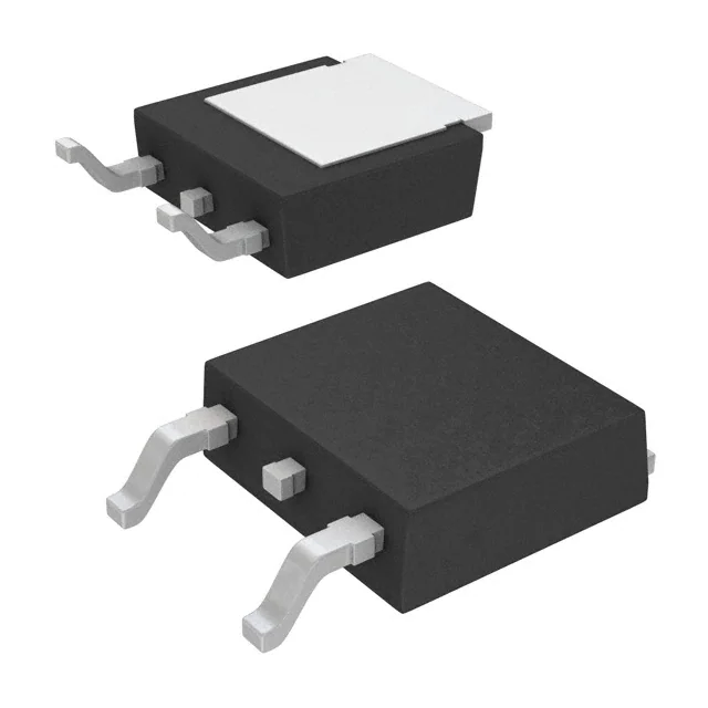


 工商网监
湘ICP备2023018690号
工商网监
湘ICP备2023018690号
