Techcode®
DATASHEET
N-Channel Enhancement Mode MOSFET
TDM3436A
DESCRIPTION
The TDM3436A uses advanced trench technology to
provide excellent RDS(ON) and low gate charge. This
device is suitable for use as a load switch or in PWM
applications.
GENERAL FEATURES
⚫
⚫
⚫
⚫
RDS(ON) < 3.2mΩ @ VGS=10V
RDS(ON) < 5.3mΩ @ VGS=4.5V
High Power and current handling capability
Lead free product is available
Surface Mount Package
Application
⚫
⚫
⚫
PWM applications
Load switch
Power management
ABSOLUTE MAXIMUM RATINGS(TJ=25℃unless otherwise noted)
Parameter
Symbol
Limit
Unit
Drain-Source Voltage
VDS
40
V
Gate-Source Voltage
VGS
+20
V
ID(TC=25℃)
89
A
ID(TC=100℃)
71
A
240
A
Avalanche Current
IDM(TC=25℃)
IAS
54
A
Single Pulse Avalanche Energy (Note 3)
EAS
145
mJ
Maximum Power Dissipation (TA=25℃) (Note 4)
PD
22
W
Maximum Operating Junction Temperature
TJ
150
℃
Storage Temperature Range
TSTG
-55 To 150
℃
Thermal Resistance Junction-to-Ambient (Note 1)
RθJA
55
℃/W
Thermal Resistance Junction-Case (Note 1)
RθJC
1.7
℃/W
Drain Current @ Continuous (Note 1)
Drain Current @ Current-Pulsed (Note 2)
THERMAL CHARACTERISTICS
January 25, 2021
Techcode Semiconductor Limited
1
www.techcodesemi.com
�Techcode®
DATASHEET
N-Channel Enhancement Mode MOSFET
TDM3436A
ELECTRICAL CHARACTERISTICS (TJ=25℃unless otherwise noted)
Parameter
Symbol
Condition
Min
Typ
Max
Unit
Drain-Source Breakdown Voltage
BVDSS
VGS=0V ID=250μA
40
-
-
V
Gate Threshold Voltage
VGS(th)
VGS=VDS, ID =250μA
1.2
1.7
2.2
V
Zero Gate Voltage Drain Current
IDSS
VDS=40V, VGS=0V
-
-
1
μA
Gate-Body Leakage Current
IGSS
VGS=±20V, VDS=0V
-
-
±100
nA
Drain-Source On-State Resistance (Note2)
RDS(ON)
VGS=10V, ID=20A
-
2.5
3.2
mΩ
VGS=4.5V, ID=15A
-
3.8
5.3
mΩ
VDS=20V,VGS=0V, F=1.0MHz
-
2648
-
PF
OFF CHARACTERISTICS
DYNAMIC CHARACTERISTICS
Input Capacitance
Ciss
Output Capacitance
Coss
-
899
-
PF
Reverse Transfer Capacitance
Crss
-
S71
-
PF
-
10
-
nS
SWITCHING CHARACTERISTICS (Note 3)
Turn-on Delay Time
td(on)
VDS=20V, VGS=10V, RG=3Ω, ID=20A
Turn-on Rise Time
tr
-
5
-
nS
Turn-Off Delay Time
td(off)
-
33
-
nS
Turn-Off Fall Time
tf
-
6.5
-
nS
Total Gate Charge
Qg
-
22.7
-
nC
Gate-Source Charge
Qgs
-
7.5
-
nC
Gate-Drain Charge
Qgd
-
5.5
-
nC
VDS=20V, ID=20A, VGS=4.5V
DRAIN-SOURCE DIODE CHARACTERISTICS
Continuous Source Current (Note 1,5)
IS
VG=VD=0V, Force Current
-
-
30
A
Diode Forward Voltage (Note 2)
VSD
VGS=0V,IS=20A
-
0.8
1.1
V
NOTES:
1. The data tested by surface mounted on a 1 inch2 FR-4 board with 2OZ copper.
2. The data tested by pulsed , pulse width ≦ 300us , duty cycle ≦ 2%
3. The EAS data shows Max. rating. The test condition is VDD=25V, VGS=10V, L=0.1mH, IAS=54A
4. The power dissipation is limited by junction temperature
5. The data is theoretically the same as ID and IDM, in real applications, should be limited by total power dissipation.
January 25, 2021
Techcode Semiconductor Limited
2
www.techcodesemi.com
�Techcode®
DATASHEET
N-Channel Enhancement Mode MOSFET
TDM3436A
Typical Operating Characteristics
January 25, 2021
Techcode Semiconductor Limited
3
www.techcodesemi.com
�Techcode®
DATASHEET
N-Channel Enhancement Mode MOSFET
TDM3436A
Typical Operating Characteristics (Cont.)
January 25, 2021
Techcode Semiconductor Limited
4
www.techcodesemi.com
�Techcode®
DATASHEET
N-Channel Enhancement Mode MOSFET
TDM3436A
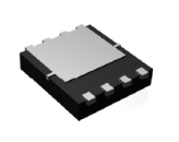
Package Information
DFN5*6-8 Package
January 25, 2021
Techcode Semiconductor Limited
5
www.techcodesemi.com
�Techcode®
DATASHEET
N-Channel Enhancement Mode MOSFET
TDM3436A
Design Notes
January 25, 2021
Techcode Semiconductor Limited
6
www.techcodesemi.com
�
很抱歉,暂时无法提供与“TDM3436A”相匹配的价格&库存,您可以联系我们找货
免费人工找货- 国内价格
- 1+2.42080
- 30+2.33180
- 100+2.15380
- 500+1.97580
- 1000+1.88680


 工商网监
湘ICP备2023018690号
工商网监
湘ICP备2023018690号
