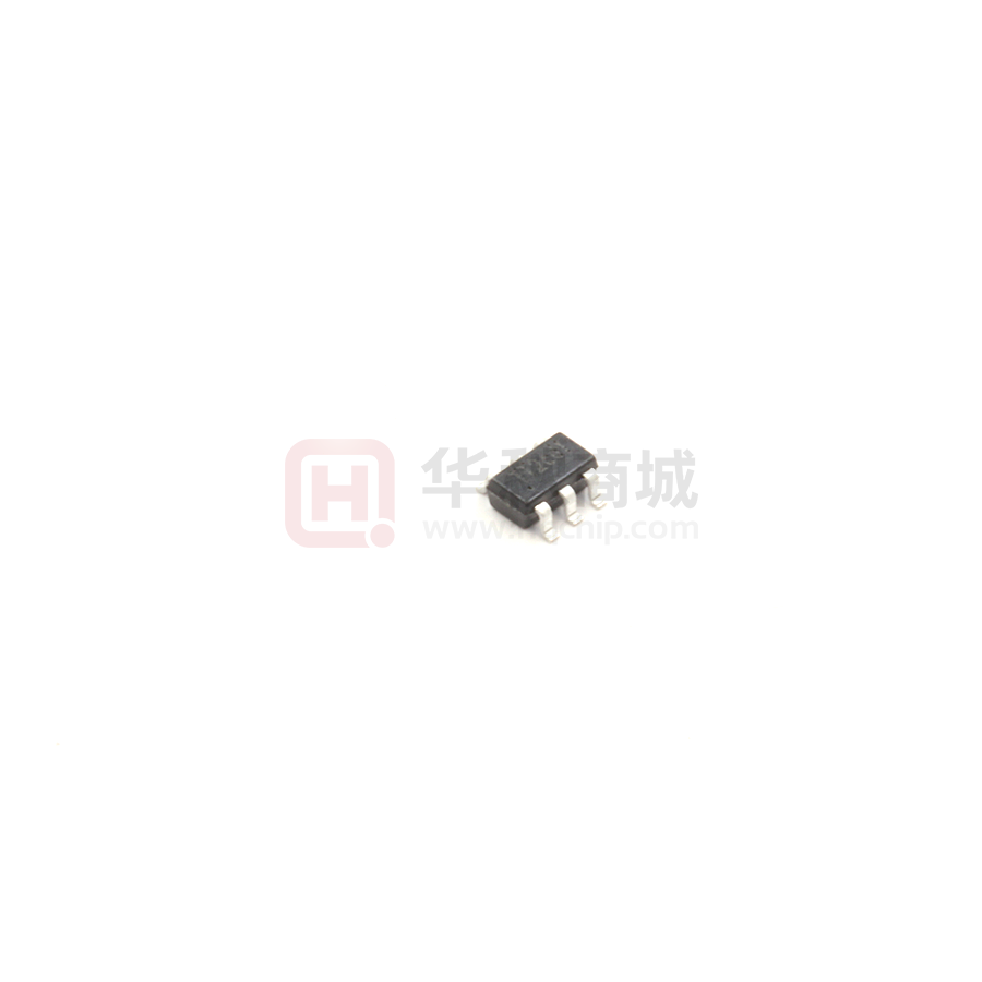
TMI3252/S/T
600kHz 18V 2A Synchronous COT Step-Down Converter
Features
Description
⚫
140mΩ/70mΩ Low RDS(ON) internal FETs
The TMI3252/S/T is a high efficiency 600kHz,
⚫
High Efficiency Synchronous-Mode
Constant on-Time (COT) control mode synchronous
Operation
step-down DC-DC converter capable of delivering
⚫
Wide Input Range:4.5V to 18V
⚫
Output Voltage from
up to 2A current. TMI3252/S/T integrates main
switch and synchronous switch with very low RDS(ON)
to minimize the conduction loss. Low output voltage
0.8V(TMI3252)
ripple and small external inductor and capacitor size
0.6V(TMI3252S)
are achieved with 600kHz switching frequency. It
0.756(TMI3252T)
adopts the COT architecture to achieve fast transient
⚫
600kHz Switch Frequency
responses for high voltage step down applications.
⚫
Up to 2A Output Current
The TMI3252 requires a minimum number of readily
⚫
COT control to achieve fast transient
available standard external components and is
responses
available in a 6-pin SOT23-6 ROHS compliant
⚫
Power Save Mode at Light Load
package.
⚫
Integrated internal compensation
Application
⚫
Stable with Low ESR Ceramic Output
⚫ Digital Set Top Boxes
Capacitors
⚫
Over Current Protection with Hiccup Mode
⚫
Thermal Shutdown
⚫
Inrush Current Limit and Soft Start
⚫
Build in Input Over Voltage Protection
⚫
Available in SOT23-6 Package
⚫ Flat Panel Television and Monitors
⚫ Notebook computer
⚫ Wireless and DSL Modems
Typical Application
Efficiency
C4
0.1µF
L
BS
CIN1
CIN2
22µF
100nF
100%
4.7µH
VOUT= 3.3V
95%
LX
R3
100kΩ
R1
39kΩ
EN
Cfb
FB
GND
90%
20pF~
100pF
CO1
R2
12.5kΩ
22µF
Efficiency
VIN
VOUT=3.3V, IOUT=0.01A to 2A, TA=25°C
85%
80%
75%
Vin=9V
Vin=12V
Vin=16V
70%
TMI3252 Typical Application Circuits (VREF=0.8V)
65%
60%
0.01
TMI and SUNTO are the brands of TOLL microelectronic
TMI3252/S/T Rev. 0.1 – 2019.02
0.1
1
Output Current (A)
10
www.toll-semi.com www.suntosemi.com
1
�TMI3252/S/T
Absolute Maximum Ratings(Note 1)
Parameter
Min
Max
Unit
Input Supply Voltage, EN
LX Voltages
FB Voltage
BS Voltage
Storage Temperature Range
Junction Temperature (Note2)
Power Dissipation
Lead Temperature (Soldering, 10s)
-0.3
-0.3
-0.3
-0.3
-65
20
20
6
23
150
V
V
V
V
°C
°C
mW
°C
160
1000
260
Package
GND 1
6 BS
BS 1
6 LX
LX 2
5 EN
GND 2
5 IN
IN 3
4 FB
FB 3
4 EN
SOT23-6
SOT23-6
Top Marking: TP2XXX / TT2XXX
Top Marking: TS2XXX
TP2/TT2: Device Code
TS2: Device Code
XXX: Inside Code
XXX: Inside Code
Order Information
Part Number
Package
Top Marking
Quantity/Reel
TMI3252
SOT23-6
TP2XXX
3000
TMI3252S
SOT23-6
TS2XXX
3000
TMI3252T
SOT23-6
TT2XXX
3000
TMI3252/TMI3252S/TMI3252T devices are Pb-free and RoHS compliant.
www.toll-semi.com www.suntosemi.com
2
TMI and SUNTO are the brands of TOLL microelectronic
TMI3252/S/T Rev.0.1 – 2019.02
�TMI3252/S/T
Pin Functions
Pin
Name
Function
TMI3252/T
TMI3252S
1
2
GND
2
6
LX
Switching Pin
3
5
IN
Power supply Pin
4
3
FB
5
4
EN
6
1
BS
Ground Pin
Output Voltage feedback input. Connect FB to the center point of the
external resistor divider.
Drive this pin to a logic-high to enable the IC. Drive to a logic-low to
disable the IC and enter micro-power shutdown mode. Don’t floating.
Bootstrap. A capacitor connected between LX and BST pins is required
to form a floating supply across the high-side switch driver.
ESD Rating
Items
Description
Value
Unit
ESD
Human Body Model for all pins
±2000
V
JEDEC specification JS-001
Recommended Operating Conditions
Items
Description
Min
Max
Unit
Voltage Range
IN
4.5
18
V
TJ
Operating Junction Temperature
-40
125
°C
Thermal Resistance (Note3)
Items
Description
Value
Unit
θJA
Junction-to-ambient thermal resistance
100
°C/W
TMI and SUNTO are the brands of TOLL microelectronic
TMI3252/S/T Rev. 0.1 – 2019.02
www.toll-semi.com www.suntosemi.com
3
�TMI3252/S/T
Electrical Characteristics (Note 4)
VIN=12V, VOUT=3.3V, TA = 25°C, unless otherwise noted.
Parameter
Conditions
Input Voltage Range
Min
Typ
4.5
OVP Threshold
Max
Unit
18
V
19.3
UVLO Rising Threshold
V
4.0
UVLO Hysteresis
Quiescent Current
VEN=2V, VFB=VREF x 105%
Shutdown Current
VIN=12V, EN=0V
V
0.45
V
300
μA
5
10
μA
Regulated Feedback Voltage(3253) TA=25°C,4.5V≤VIN≤18V
0.784
0.8
0.816
V
Regulated Feedback Voltage(3253S) TA=25°C,4.5V≤VIN≤18V
0.588
0.6
0.612
V
Regulated Feedback Voltage(3253T) TA=25°C,4.5V≤VIN≤18V
0.750
0.765
0.780
V
High-Side Switch On-Resistance
140
mΩ
Low-Side Switch On-Resistance
70
mΩ
High-Side Switch Leakage Current
VEN=0V, VLX=0V
Switch Valley Current Limit
Minimum Duty Cycle
On Time
VIN=12V, VOUT=1.2V, IOUT=1A
1
10
3
132
166
μA
A
200
ns
Oscillation Frequency
600
kHz
Maximum Duty Cycle
65
%
Minimum On-Time
80
ns
Soft Start Time
1
ms
Hiccup on Time
1.4
ms
4
ms
Hiccup Time Before Restart
EN High-Level Input Voltage
1.5
V
EN Low-Level Input Voltage
0.3
V
Thermal Shutdown Hysteresis (Note 4)
165
°C
Thermal Shutdown Hysteresis (Note 4)
30
°C
Note 1: Absolute Maximum Ratings are those values beyond which the life of a device may be
impaired.
Note 2: TJ is calculated from the ambient temperature TA and power dissipation PD according to the
following formula: TJ = TA + PD x θJA. The maximum allowable continuous power dissipation at any
ambient temperature is calculated by PD (MAX) = (TJ(MAX)-TA)/θJA.
Note 3: Measured on JESD51-7, 4-layer PCB.
Note 4: Thermal shutdown threshold and hysteresis are guaranteed by design.
www.toll-semi.com www.suntosemi.com
4
TMI and SUNTO are the brands of TOLL microelectronic
TMI3252/S/T Rev.0.1 – 2019.02
�TMI3252/S/T
Block Diagram
EN
VIN
BS
Regulator
UVLO
OVP
Vuv
+
OTP
Hiccup
-
FB
+ EA
+
Voltage
Reference
LX
Logic
Control
PWM Comparator
Gate
Driver
VCOMP
+
-
ON time
Generater
+
ZC
-
Soft Start
Current Sense
and OCP
GND
Figure 1. TMI3252/S/T Block Diagram
Operation Description
Internal Regulator
The TMI3252/S/T is a constant on-time (COT) step down DC/DC converter that provides excellent
transient response with no extra external compensation components. This device contains low resistance,
high voltage high side and low side power MOSFETs, and operates at 600kHz operating frequency to
ensure a compact, high efficiency design with excellent AC and DC performance.
Error Amplifier
TMI3252/S/T adopts operational transconductance amplifier (OTA) as error amplifier. The error amplifier
compares the FB pin voltage with the internal FB reference (VREF) and outputs a current proportional to
the difference between the two. This output current is then used to charge or discharge the internal
compensation network to form the VCOMP voltage, which is used to compare with the low side power
MOSFET current sensing signal and trigger on time pulse. The optimized internal compensation network
minimizes the external component counts and simplifies the control loop design.
TMI and SUNTO are the brands of TOLL microelectronic
TMI3252/S/T Rev. 0.1 – 2019.02
www.toll-semi.com www.suntosemi.com
5
�TMI3252/S/T
Internal Soft-Start
The soft-start is implemented to prevent the converter output voltage from overshooting during startup.
When the chip starts, the internal circuitry generates a soft-start voltage (SS) ramping up from 0V to VREF.
When it is lower than the internal FB reference (VREF), SS overrides REF so the error amplifier uses SS
as the reference. When SS is higher than VREF, VREF regains control. The SS time is internally fixed to
1ms typically.
Over-Current-Protection and Short Circuits Protection
The TMI3252/S/T has cycle-by-cycle valley current limit function. When the inductor current valley value
is larger than the valley current limit during low side MOSFET on state, the device enters into valley over
current protection mode and low side MOSFET keeps on state until inductor current drops down to the
value equal or lower than the valley current limit, and then on time pulse could be generated and high
side MOSFET could turn on again.
If the output is short to GND and the output voltage drop until feedback voltage VFB is below the output
under-voltage VUV threshold which is typically 45% of VREF, TMI3252/S/T enters into hiccup mode to
periodically disable and restart switching operation. The hiccup mode helps to reduce power dissipation
and thermal rise during output short condition. The period of TMI3252/S/T hiccup mode is typically 5.4ms.
Startup and Shutdown
If both VIN and EN are higher than their appropriate thresholds, the chip starts switching operation. The
reference block starts first, generating stable reference voltage and currents, and then the internal
regulator is enabled. The regulator provides stable supply for the remaining circuitries. Three events can
shut down the chip: EN low, VIN low and thermal shutdown. In the shutdown procedure, the signaling
path is first blocked to avoid any fault triggering. The VCOMP voltage and the internal supply rail are then
pulled down. The floating driver is not subject to this shutdown command.
Application Information
Setting the Output Voltage
The external resistor divider is used to set the output voltage (see Typical Application on page 1). Choose
R1 to be around 39kΩ for optimal transient response. R2 is then given by:
Table 1: Selection for Common Output Voltages(VFB=0.8V)
VOUT (V)
R1 (kΩ)
R2 (kΩ)
CFB(pF)
L (μH)
5
39
7.43
33
4.7
3.3
39
12.5
33
4.7
2.5
39
18.3
33
3.3
1.8
39
31.2
33
2.2
1.5
39
44.6
33
2.2
1.2
39
78
33
1.5
1
18
72
33
1.0
www.toll-semi.com www.suntosemi.com
6
R2 =
R1
Vout /VFB − 1
C fb=20pF~100pF
TMI3252
VOUT
FB
R1
R2
Figure 2. Feedback Network
TMI and SUNTO are the brands of TOLL microelectronic
TMI3252/S/T Rev.0.1 – 2019.02
�TMI3252/S/T
Selecting the Inductor
A 1.0μH to 4.7μH inductor with a DC current rating of at least 25% percent higher than the maximum load
current is recommended for most applications. For highest efficiency, the inductor DC resistance should
be as small as possible. For most designs, the inductance value can be derived from the following
equation.
V (Vin − Vout )
L = out
Vin I L fOSC
Where ΔIL is the inductor ripple current. Choose inductor ripple current to be approximately 30% if the
maximum load current, 3A. The maximum inductor peak current is:
I L ( MAX ) = I LOAD +
I L
2
Under light load conditions below 100mA, larger inductance is recommended for improved efficiency.
Selecting the Output Capacitor
The output capacitor (Co1) is required to maintain the DC output voltage. Ceramic, tantalum, or low
ESR electrolytic capacitors are recommended. Low ESR capacitors are preferred to keep the output
voltage ripple low. The output voltage ripple can be estimated by:
VOUT =
VOUT VOUT
1
1 −
RESR +
f S L VIN
8 f S C2
Where L is the inductor value and RESR is the equivalent series resistance (ESR) value of the output
capacitor. In the case of ceramic capacitors, the impedance at the switching frequency is dominated by
the capacitance. The output voltage ripple is mainly caused by the capacitance. For simplification, the
output voltage ripple can be estimated by:
VOUT =
V
1 − OUT
8 f S L C 2 VIN
VOUT
2
In the case of tantalum or electrolytic capacitors, the ESR dominates the impedance at the switching
frequency. For simplification, the output ripple can be approximated to:
VOUT =
VOUT VOUT
1 −
RESR
f S L VIN
The characteristics of the output capacitor also affect the stability of the regulation system. The
TMI3252/S/T can be optimized for a wide range of capacitance and ESR values.
TMI and SUNTO are the brands of TOLL microelectronic
TMI3252/S/T Rev. 0.1 – 2019.02
www.toll-semi.com www.suntosemi.com
7
�TMI3252/S/T
Typical Performance Characteristics
Efficiency
Efficiency
VOUT =5V, L=4.7μH, DCR=30mΩ
100%
100%
95%
95%
90%
90%
85%
85%
Efficiency
Efficiency
VOUT =3.3V, L=4.7μH, DCR=30mΩ
80%
75%
Vin=9V
Vin=12V
Vin=16V
70%
65%
80%
75%
Vin=9V
Vin=12V
Vin=16V
70%
65%
60%
60%
0.01
0.1
1
Output Current (A)
10
0.01
0.1
1
Output Current (A)
Efficiency
10
Load Regulation
VOUT=1.2V, L=2.2μH, DCR=20mΩ
VIN=12V, TA=25°C
100%
1.5%
90%
1.0%
Vout=3.3V
0.5%
Vout=5V
Output Regulation (%)
Vout=1.2V
Efficiency
80%
70%
60%
Vin=9V
50%
Vin=12V
0.01
0.1
1
Output Current (A)
-0.5%
-1.0%
-1.5%
Vin=16V
40%
0.0%
10
0
Steady State Operation
0.5
1
Output Current (A)
1.5
2
Steady State Operation
VIN =12V, VOUT =3.3V, No Load
VIN =12V, VOUT =3.3V, Io=2A
Vout=20mV/div
AC coupled
Vout=20mV/div
AC coupled
LX=10V/div
LX=10V/div
Vin=50mV/div
AC coupled
Vin=50mV/div AC coupled
IL=500mA/div
IL=2A/div
Time: 2μs/div
www.toll-semi.com www.suntosemi.com
8
Time: 1μs/div
TMI and SUNTO are the brands of TOLL microelectronic
TMI3252/S/T Rev.0.1 – 2019.02
�TMI3252/S/T
Typical Performance Characteristics(continued)
Load Transient
Load Transient
VIN =12V, VOUT =3.3V, Io =0A to 1A
VIN =12V, VOUT =3.3V, Io =1A to 2A
Vout=200mV/div
AC coupled
Vout=200mV/div
AC coupled
Io=1A/div
Io=1A/div
Time: 400μs/div
Time: 400μs/div
Output Short Entry
Output Short Recovery
VIN =12V, VOUT =3.3V, No Load
VIN=12V, VOUT =3.3V, No Load
Vout=2V/div
Vout=2V/div
Vin=5V/div
Vin=5V/div
LX=10V/div
LX=10V/div
IL=2 A/div
Time: 4ms/div
IL=2A/div
Input Power On
Time: 4ms/div
Input Power Down
VIN =12V, VOUT =3.3V, Io = 2A
VIN =12V, VOUT =3.3V, Io = 2A
Vout=2V/div
Vout=2V/div
Vin=5V/div
LX=10V/div
Vin=5V/div
LX=10V/div
IL=2A/div
TMI and SUNTO are the brands of TOLL microelectronic
TMI3252/S/T Rev. 0.1 – 2019.02
Time: 10ms/div
IL=2A/div
Time: 400μs/div
www.toll-semi.com www.suntosemi.com
9
�TMI3252/S/T
Typical Performance Characteristics(continued)
EN Enable
EN Disable
VIN =12V, VOUT =3.3V, Io =Full Load
VIN =12V, VOUT =3.3V, Io =Full Load
Vout=2V/div
Vout=2V/div
LX=10V/div
LX=10V/div
EN=5V/div
EN=5V/div
IL=1A/div
Time: 400μs/div
IL=1A/div
Time: 40μs/div
Typical Application Circuits
C4
0.1µF
L
BS
VIN
CIN1
CIN2
22µF
100nF
4.7µH
VOUT=5V
LX
R3
100kΩ
R1
39kΩ
EN
Cfb
20pF~
100pF
FB
CO1
R2
7.43kΩ
GND
22µF
Figure 4. 12VIN, 5V Output (VFB=0.8V)
C4
0.1µF
L
BS
VIN
CIN1
CIN2
22µF
100nF
4.7µH
VOUT= 3.3V
LX
R3
100kΩ
R1
39kΩ
Cfb
20pF~
100pF
EN
FB
GND
CO1
R2
12.5kΩ
22µF
Figure 5. 12VIN, 3.3V Output (VFB=0.8V)
www.toll-semi.com www.suntosemi.com
10
TMI and SUNTO are the brands of TOLL microelectronic
TMI3252/S/T Rev.0.1 – 2019.02
�TMI3252/S/T
Typical Application Circuits(continued)
C4
0.1µF
6
CIN1
CIN2
22µF
100nF
2
BS
3
L 2.2µH
VOUT= 1.8V
LX
VIN
R3
100kΩ
R1
39kΩ
5
Cfb
20pF~
100pF
4
FB
EN
CO1
R2
31.2kΩ
GND
1
22µF
Figure 6. 12VIN, 1.8V Output (VFB=0.8V)
C4
0.1µF
6
BS
3
CIN1
CIN2
22µF
100nF
VIN
2
L 2.2µH
VOUT= 1.5V
LX
R3
100kΩ
Cfb
R1
39kΩ
5
20pF~
100pF
4
EN
FB
CO1
R2
44.6kΩ
GND
1
22µF
Figure 7. 12VIN, 1.5V Output (VFB=0.8V)
C4
0.1µF
6
3
CIN1
CIN2
22µF
100nF
BS
VIN
2
L 1.5µH
VOUT= 1.2V
LX
R3
100kΩ
R1
39kΩ
5
20pF~
100pF
4
EN
Cfb
FB
GND
1
CO1
R2
78kΩ
22µF
Figure 8. 12VIN, 1.2V Output (VFB=0.8V)
TMI and SUNTO are the brands of TOLL microelectronic
TMI3252/S/T Rev. 0.1 – 2019.02
www.toll-semi.com www.suntosemi.com
11
�TMI3252/S/T
Typical Application Circuits(continued)
C4
0.1µF
6
3
CIN1
CIN2
22µF
100nF
BS
VIN
2
L
1µH
VOUT= 1V
LX
R3
100kΩ
R1
18kΩ
5
20pF~
100pF
4
EN
Cfb
FB
GND
1
CO1
R2
72kΩ
22µF
Figure 9. 12VIN, 1V Output (VFB=0.8V)
www.toll-semi.com www.suntosemi.com
12
TMI and SUNTO are the brands of TOLL microelectronic
TMI3252/S/T Rev.0.1 – 2019.02
�TMI3252/S/T
PCB Layout Guide
PCB layout is very important to achieve stable operation. It is highly recommended to duplicate EVB
layout for optimum performance. If change is necessary, please follow these guidelines and take Figure
3 for reference.
1) Keep the path of switching current short and minimize the loop area formed by Input capacitor, IN pin
and GND.
2) Bypass ceramic capacitors are suggested to be put close to the IN Pin.
3) Ensure all feedback connections are short and direct. Place the feedback resistors as close to the chip
as possible.
4) VOUT, LX away from sensitive analog areas such as FB.
5) Connect IN, LX, and especially GND respectively to a large copper area to cool the chip to improve
thermal performance and long-term reliability.
Top Layer
Bottom Layer
VOUT
VIN
LX
Figure 3. Sample of PCB Layout (TMI3252)
TMI and SUNTO are the brands of TOLL microelectronic
TMI3252/S/T Rev. 0.1 – 2019.02
www.toll-semi.com www.suntosemi.com
13
�TMI3252/S/T
Package Information
SOT23-6
Unit: mm
Dimensions In Millimeters
Symbol
Min
Typ
Max
Min
Typ
Max
A
2.80
2.90
3.00
L3
1.800
1.900
2.000
B
2.60
2.80
3.00
L4
0.077
0.127
0.177
B1
1.50
1.60
1.70
L5
-
0.250
-
C
-
-
1.05
L6
-
0.600
-
C1
0.60
0.80
1.00
θ
0°
C2
0.35
0.40
0.45
Θ1
10°
12°
14°
C4
0.223
0.273
0.323
Θ2
10°
12°
14°
K
0.000
0.075
0.150
R
-
0.100
-
L
0.325
0.400
0.475
R1
-
0.100
-
L1
0.325
0.450
0.550
R2
-
0.100
-
L2
0.850
0.950
1.050
www.toll-semi.com www.suntosemi.com
14
Dimensions In Millimeters
Symbol
0°
TMI and SUNTO are the brands of TOLL microelectronic
TMI3252/S/T Rev.0.1 – 2019.02
�TMI3252/S/T
Tape and Reel Information
Tape Dimensions:
Reel Dimensions:
Note:
1)
All Dimensions are in Millimeter.
2)
Quantity of Units per Reel is 3000.
3)
MSL level is level 3.
TMI and SUNTO are the brands of TOLL microelectronic
TMI3252/S/T Rev. 0.1 – 2019.02
www.toll-semi.com www.suntosemi.com
15
�


 工商网监
湘ICP备2023018690号
工商网监
湘ICP备2023018690号